摄像头模块资料
OV7670 摄像头模块介绍

OV7670 摄像头模块介绍OV7670 摄像头模块简介OV7670是OV(OmniVision)公司生产的一颗1/6寸的CMOS VGA 图像传感器。
该传感器体积小、工作电压低,提供单片VGA摄像头和影像处理器的所有功能。
通过SCCB 总线控制,可以输出整帧、子采样、取窗口等方式的各种分辨率8位影像数据。
该产品VGA图像最高达到30帧/秒。
用户可以完全控制图像质量、数据格式和传输方式。
所有图像处理功能过程包括伽玛曲线、白平衡、度、色度等都可以通过SCCB接口编程。
OmmiVision 图像传感器应用独有的传感器技术,通过减少或消除光学或电子缺陷如固定图案噪声、托尾、浮散等,提高图像质量,得到清晰的稳定的彩色图像。
OV7670 摄像头模块特点1、高灵敏度、低电压适合嵌入式应用。
2、标准的SCCB接口,兼容IIC接口。
3、支持RawRGB、RGB(GBR4:2:2,RGB565/RGB555/RGB444),YUV(4:2:2)和YCbCr(4:2:2)输出格式。
4、支持VGA、CIF,和从CIF到40*30的各种尺寸输出。
5、支持自动曝光控制、自动增益控制、自动白平衡、自动消除灯光条纹、自动黑电平校准等自动控制功能。
同时支持色饱和度、色相、伽马、锐度等设置。
6、支持闪光灯。
7、支持图像缩放。
OV7670 摄像头模块功能框图OV7670传感器包括如下一些功能模块。
1、感光整列(Image Array)OV7670总共有656*488个像素,其中640*480个有效(即有效像素为30W)。
2、时序发生器(Video Timing Generator)时序发生器具有的功能包括:整列控制和帧率发生(7种不同格式输出)、内部信号发生器和分布、帧率时序、自动曝光控制、输出外部时序(VSYNC、HREF/HSYNC和PCLK)。
3、模拟信号处理(Analog Processing)模拟信号处理所有模拟功能,并包括:自动增益(AGC)和自动白平衡(AWB)。
OV5640 摄像头模块用户手册说明书

OV5640 Camera Board (B)USER MANUALOVERVIEWThe module OV5640 Camera Board (B) contains is a video camera based on video sensor OV5640 (CMOS), takes 5 Megapixel image in QSXGA mode (2592x1944), uses DVP data interface and SCCB control interface. It supports RGB565\RGB555\RGB444, YUV(422/420), YCbCr422 and JPEG pixel/image formats. The module can adjust white balance, saturation, hue, sharpness, and gamma correction. The resolution and frame rate are adjustable as well. The view angle is 170° that is suitable for security monitoring.FEATURES•Number of pixels: 5M•Highest resolution: 2592x1944•Video sensor: OV5640o uses 1.4 x 1.4 um pixels OmniBSI technology, high sensitivity, low crosstalk and noiseo supports automatic exposure, white balance, elimination of light stripes, black level calibration, band pass filter, and other automatic functionso supports adjustment of saturation, hue, gamma correction, sharpness, and lens calibration, etco supports zoom, window parallel translation and window settings•Camera:o CCD size: 1/4 incheso Aperture (F): 3.0o Focal Length: 3.8mmo View angle (diagonal): 170 degrees•Output modes:o YUV (422/420)/YCbCr422o RGB565/555/444o CCIR656o RAW RGBo Compressed Data•Operating voltage: 3.3V•Control interface: SCCB (compatible with I2C)•Data interface: DVP 8-bits•Size: 35.70 mm × 23.90 mmINTERFACE DESCRIPTIONOV5640 Camera Board (B) Pin descriptions3.3V Power input 3.3VGND GroundSIOC SCCB clock signalSIOD SCCB data signalVSYNC Frame synchronization signalHREF Line synchronization signalPCLK Pixel clockXCLK External oscillator clock inputD0 ~ D7 Pixel data outputRST Reset (active low)PWDN Save energy mode (high effective)SCCB CONTROL INTERFACESCCB (Serial Camera Control Bus) is a serial control bus of a camera. SCCB is similar to I2C, because start and stop signals are same as in I2C, SCCB defines basic data transfer unit (phase), each phase of data transfer takes one byte. SCCB contains only three kinds of transmission cycle:1)3-phase write transmission cycle3-phase cycle includes: device address, register address, data2)2-phase write transmission cycle2-phase cycle includes: device address, register address3)2-phase write transmission cycle2-phase cycle includes: device address, dataWhile writing: use 3-phase write cycle directlyWhile Reading: first use 2-phase write cycle, then use 2-phase read cycleMore detailed information about SCCB protocol see in “OmniVision Technologies Serial Camera Control Bus (SCCB) Specification”DVP DATA INTERFACEThe module OV5640 uses DVP data transfer interface, because camera driver interface (DCMI) in our STM32F407\429\746 boards only supports DVP. OV5640 sensor has 10-bits DVP interface, but we usually use 8-bits data processing. For example, in the following picture there are: OV5640 8 highest bits at the left side connected to 8 bits of STM32F407\429\746 board at the right site.DVP interface timing diagram:DCMI INTERFACEDCMI (Digital camera media interface) is digital camera interface, integrated intoSTM32F4xx, F7xx series of MCU. DCMI is synchronous parallel interface, capable receive 8-, 10-, 12- or 14-bits data stream from CMOS camera module. It can support various data modes: YCbCr422, RGB565 and compressed data (JPEG).DCMI interface can support input data stream speed up to 54 MB/s. The interface contains 14 data pins (D13-D0) and pixel clock pin (PIXCLK). The pixel clock polarity can be programmed and therefore data can be caught at the rising or falling front. These data come to 32-bit register (DCMI_DR), and then are transmitted via DMA. The image buffer is controlled by DMA, not by camera interface. Data received from camera can be restored to original image lines of frames (YUB/RGB modes) or series of JPEG files. To enable receiving JPEG images the JPEG bit (the 3rd DCMI_CR bit) must be set to 1. Data stream can be synchronized by HSYNC (horizontal synchronization) signal and VSYNC (vertical synchronization) signal, otherwise by synchronization signals embedded into the data stream.DCMI block diagram:Top-level block diagram:The DMA interface active when the CAPTURE bit of DCMI_CR is set to 1. Every time the camera receive full 32-bits block will trigger a DMI request.More detailed information about SCCB protocol see in datasheetUSAGE DESCRIPTIONThis module provides STM32F407\429\746 routines, here are demonstration examples for Waveshare Open746I-C development board:1. Connect the module to DCMI port of the development board, connect USB-to-serial adapter to USART1 serial port on the board and to USB port on computer.2. Open UartDisplay (camera data receiving software) on your computer, set number of port and its rate 921600, and the open the port.3. Download the program into the board, push RESET button and after some initialization period it shows following data:4. Push WAKE UP button and the board will start to sent continuously JPEG images via serial port and UartDisplay will show them.5. Push middle key of the board’s joystick and OV5640 m odule will keep image on LCD screen in RGB565 mode continuouslyOpen746I-C+7inch LCDOpen746I-C+4.3inch LCDOpen407V-C+3.2inch LCD。
8MP Sony IMX219 USB摄像头模块说明书
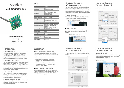
8MP Sony IMX219(SKU:B0196)QUICK START GUIDEUSB Camera ModuleSPECSHow to use the program (Windows demo only)The Menu bar at the top of the shown image con-tains few menu items and the current preview resolution and the frame rate are displayed on the bottom bar when the application is running. The following sections describe each of the menu items•Menu>DevicesThis menu will show the available video devices to host PC. The B0196 named USB Camera .•Menu>OptionsThe options menu can be used to select the pre-view and image parameters supported by this camera.How to use the program (Windows demo only)-Video Capture PinINTRODUCTION•About ArducamArducam has been a professional designer and manufacturer of SPI, MIPI, DVP and USB cameras since 2012. We also offer customized turnkey design and manufacturing solution services for customers who want their products to be unique.•About this USB CameraThe B0196 is a new member of the Arducam ’s USB camera family. It ’s an 8MP, UVC compliant, USB 2.0 camera. This USB camera is based on 1/4” Sony IMX219 image sensor, and you can learn more about its specs in the next chapter. Arducam also provides the sample application that demonstrates some features of this camera.•About UVCThe B0196 is a UVC -compliant camera. The native UVC drivers of Windows, Linux and Mac shall be compatible with this camera so that it does not require extra drivers to be installed.•About Customer ServiceIf you need our help or want to customize other models of USB cameras, feel free to contact us at *******************QUICK START•How to download the program1.Download the APP Amcap from the following link https:///downloads/app/AMCap.exe2.NOTE:If used with the Android device, USB Camera APP and connect adapter are needed.For Mac OS, please open the native software facetime and select the video camera “USB Camera” .•How to connect the cameraConnect the one end of the USB 2.0 cable to the USB 2.0 connector provided on the back of B0196, and connect the other end to the USB 2.0 host controller on the computer.How to use the program (Windows demo only)-Video Capture Filter -> Video Proc Amp/Camera ControlHow to use the program (Windows demo only)•Menu> CaptureThe capture menu is used to capture the still image and video by using this application. You can also select the related parameters.。
摄像头模块工作原理

摄像头模块工作原理
摄像头模块是一种用于捕捉图像和视频的设备。
它由镜头、图像传感器、信号处理芯片和接口电路等组成。
工作原理如下:
1. 光线投射:当环境中有光线时,镜头会将光线聚焦到图像传感器上。
2. 传感器感应:图像传感器是一种电子器件,它可以将通过镜头传来的光线转换为电信号。
图像传感器一般采用CMOS或CCD技术,其中CMOS传感器成本低、功耗低、制造工艺简单,而CCD传感器具有更高的感光度和图像质量。
3. 信号处理:经过图像传感器转换的电信号会被送入信号处理芯片。
信号处理芯片负责对电信号进行放大、滤波、去噪等处理,以提高图像的质量和清晰度。
4. 数据输出:经过信号处理后,图像数据会通过接口电路输出到计算机、显示屏或其他设备上进行显示、存储或传输。
总结来说,摄像头模块通过将光线聚焦到图像传感器上,再通过信号处理将图像转换为电信号并进行处理,最后将处理后的图像数据输出到其他设备上。
这样就能实现图像和视频的捕捉、显示和传输。
摄像头模组(CCM)介绍:
摄像头模组(CCM)介绍:⼀、摄像头模组(CCM)介绍:1、camera特写摄像头模组,全称CameraCompact Module,以下简写为CCM,是影像捕捉⾄关重要的电⼦器件。
先来张特写,各种样⼦的都有,不过我前⼀段时间调试那个有点丑。
2、摄像头⼯作原理、camera的组成各组件的作⽤想完全的去理解,还得去深⼊,如果是代码我们就逐步分析,模组的话我们就把它分解开来,看他到底是怎么⼯作的。
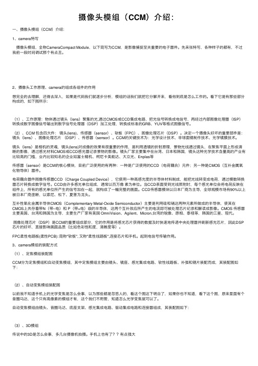
看下它是有那些部分构成的,如下图所⽰:(1)、⼯作原理:物体通过镜头(lens)聚集的光,通过CMOS或CCD集成电路,把光信号转换成电信号,再经过内部图像处理器(ISP)转换成数字图像信号输出到数字信号处理器(DSP)加⼯处理,转换成标准的GRB、YUV等格式图像信号。
(2)、CCM 包含四⼤件:镜头(lens)、传感器(sensor)、软板(FPC)、图像处理芯⽚(DSP)。
决定⼀个摄像头好坏的重要部件是:镜头(lens)、图像处理芯⽚(DSP)、传感器(sensor)。
CCM的关键技术为:光学设计技术、⾮球⾯镜制作技术、光学镀膜技术。
镜头(lens)是相机的灵魂,镜头(lens)对成像的效果有很重要的作⽤,是利⽤透镜的折射原理,景物光线通过镜头,在聚焦平⾯上形成清晰的影像,通过感光材料CMOS或CCD感光器记录景物的影像。
镜头⼚家主要集中在台湾、⽇本和韩国,镜头这种光学技术含量⾼的产业有⽐较⾼的门槛,业内⽐较知名的企业如富⼠精机、柯尼卡美能达、⼤⽴光、Enplas等传感器(sensor)是CCM的核⼼模块,⽬前⼴泛使⽤的有两种:⼀种是⼴泛使⽤的CCD(电荷藕合)元件;另⼀种是CMOS(互补⾦属氧化物导体)器件。
电荷藕合器件图像传感器CCD(Charge Coupled Device),它使⽤⼀种⾼感光度的半导体材料制成,能把光线转变成电荷,通过模数转换器芯⽚转换成数字信号。
CCD由许多感光单位组成,通常以百万像素为单位。
摄像头模组基础知识扫盲
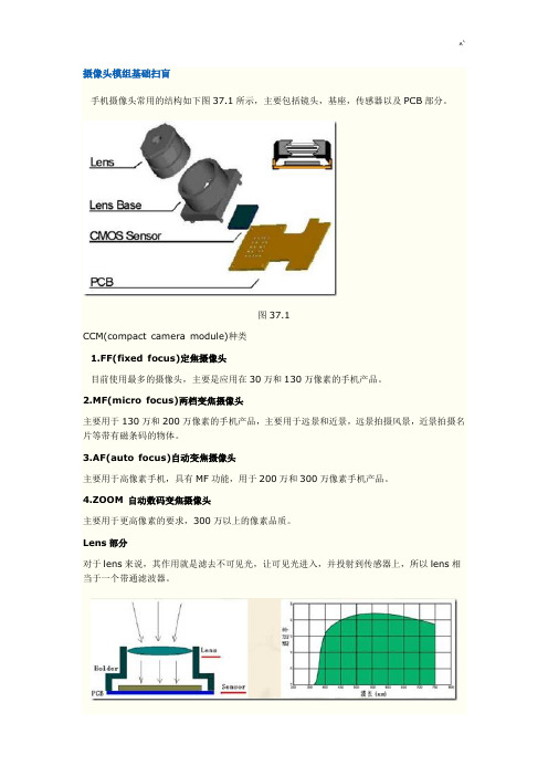
摄像头模组基础扫盲手机摄像头常用的结构如下图37.1所示,主要包括镜头,基座,传感器以及PCB部分。
图37.1CCM(compact camera module)种类1.FF(fixed focus)定焦摄像头目前使用最多的摄像头,主要是应用在30万和130万像素的手机产品。
2.MF(micro focus)两档变焦摄像头主要用于130万和200万像素的手机产品,主要用于远景和近景,远景拍摄风景,近景拍摄名片等带有磁条码的物体。
3.AF(auto focus)自动变焦摄像头主要用于高像素手机,具有MF功能,用于200万和300万像素手机产品。
4.ZOOM 自动数码变焦摄像头主要用于更高像素的要求,300万以上的像素品质。
Lens部分对于lens来说,其作用就是滤去不可见光,让可见光进入,并投射到传感器上,所以lens相当于一个带通滤波器。
CMOS Sensor部分对于现在来说,sensor主要分为两类,一类是CMOS,一类是CCD,而且现在CMOS是一个趋势。
对于镜头来讲,一个镜头只能适用于一种传感器,且一般镜头的尺寸应该和sensor的尺寸一致。
对于sensor来说,现在仍然延续着Bayer阵列的使用,如下图37.2所示,图37.3展示了工作流程,光照à电荷à弱电流àRGB信号àYUV信号。
图37.2图37.3图37.4图37.4展示了sensor的工作原理,这和OV7670以及OV7725完全相同。
像素部分那么对于像素部分,我们常常听到30万像素,120万像素等等,这些代表着什么意思呢?图37.5解释了这些名词。
图37.5那么由上面的介绍,可以得出,我们以30万像素为例,30万像素~= 640 * 480 = 3 0_7200;可见所谓的像素数也就是一帧图像所具有的像素点数,我们可以联想图像处理的相关知识,这里的像素点数的值,也就是我们常说的灰度值。
像素数越高,当然显示的图像的质量越好,图像越清晰,但相应的对存储也提出了一定的要求,在图像处理中,我们也会听到一个概念,叫做分辨率,其实这个概念应该具体化,叫做图像的空间分辨率,例如72ppi,也就是每英寸具有72个像素点,比较好的相机,能达到490ppi。
2.4g摄像头无线模块说明书

深圳市凌承芯电子有 函数说明
(1) UINT8 SPI_RW(UINT8 value) 描述:通过 SPI 的 MOSI 线向芯片写入 8 个 bit 数,并从 MISO 线上获取 8 个 bit。 参数:value: 向 MOSI 线上输出的 8bit 数 返回值:从 MISO 线上获取的 8bit 数
SwitchToRxMode
切换芯片到 RX 模式
SwitchToTxMode
切换芯片到 TX 模式
TR24_Initialize
芯片初始化,并进入到 RX 模式
Send_Packet
发送包
Receive_Packet
接受包
SetChannelNum
设置新频点
SwitchCFG
切换到 Bank1 寄存器操作,仅为载波测试、
(6) void SwitchToRxMode() 描述:将芯片切换为接收模式。 参数:无 返回值:无
(7) void SwitchToTxMode() 描述:将芯片切换为发送模式。 输入:无 返回值:无
(8) void TR24_Initialize() 描述:完成芯片初始化,配置所有寄存器,并切换为接收模式。 参数:无
Set_LowPower_Mode
芯片进入低输出 power 模式
Close_CD_Detect
如果不需要 CD 功能,可以关闭该功能,减少
大约 1mA 电流
Get_Chip_ID
得到芯片的 ID 号
注:背景带蓝色的部分涉及到读写 Bank1 的寄存器,建议客户根据需要直接使用或者移植相
关代码。
lchstarsales@
lchstarsales@
深圳市凌承芯电子有限公司
摄像头模组基础知识--CameraModule(COMS与CCD)

摄像头模组基础知识--CameraModule(COMS与CCD)1) Camera Module构成摄像头模组的整体2D图纸,主要介绍摄像头模组的尺寸,弯折状态,连接器型号,sensor型号等。
- Sensor Chip晶片sensor chipsensor 电路以及连接器电路FPC摄像头模组实物CMOS 与CCD摄像头的差异:CMOS(Complementary Metal-Oxide Semiconductor)即互补性金属氧化物半导体,其在微处理器、闪存和特定用途集成电路(ASIC)的半导体技术上占有绝对重要的地位。
CMOS和CCD一样都是可用来感受光线变化的半导体。
CMOS主要是利用硅和锗这两种元素所作成的半导体,通过CMOS上带负电和带正电的晶体管来实现基本的功能的。
这两个互补效应所产生的电流即可被处理芯片记录和解读成影像。
CCD 是英语 Charge Coupled Device(电荷耦合元件)的缩写,是一种将图像转换为电信号的半导体元件。
大小约为长宽各1 厘米左右,由类似棋盘的格状排列的小像素 (pixel) 组成。
CCD Image Sensor (Charged Coupled Device,电荷耦合元件)在光转换部存储的光电荷由Analog Shift Register传送的方式这是在各cell中存储的电荷由电压差形成的cell完成Shift.比CMOS Sensor集成度和传送速度低,但能得到高的图像质量的元件.数字摄像机的 CCD (Charge Coupled Device)是把光信号转换为电信号的作用,并由很多元件构成把这些元件表示为pixei或像素.CCD的大小是把对角线的直径1/2inch, 1/3inch来表示为对角线的直径,应把总像素数和有效像素数分开表示是正确Power 消耗指对CCD的情况表示在CCD中消耗的功率, 而对CIS的情况输出Digital out put (内装ADC)的情况.观察其他特征时, CCD的情况比CMOS的工序相对难, CMOS的情况可以random access而CCD是不可以的. 20世纪90年代后期及最近,由于CMOS工序技术的发展和signal processing algorithm(运算法则)的改善等开始克服了已有的CMOS Image Sensor具有的不足,又选择性地把CCD工序使用CMOS Image Sensor上,使制品质量比现有的改善的特别其技术力量快速增加把Image Sensor市场的实际情况达到与CCD平分的程度.。
摄像头模块原理
摄像头模块原理
摄像头模块是一种通过光学传感器和图像处理器来捕获和处理图像的设备。
它通常由镜头、感光元件、转换器、接口电路和处理器等组成。
工作原理:摄像头的镜头通过对场景进行聚焦,将光线通过感光元件投射在其表面上。
感光元件通常采用CMOS或CCD技术,能够将光信号转换为电信号。
转换器将电信号转换为数字信号,以获得更好的图像质量。
接口电路将数字信号传输至处理器,处理器会对信号进行压缩编码、图像滤波、色彩增强、曝光调节和白平衡等处理,以优化图像质量。
处理器还可以实现功能如自动对焦、人脸识别、动态范围调节和视频录制等。
摄像头模块通常通过串行总线接口(如I2C或SPI)与主控制器进行通信,并获取主控制器发送的命令。
主控制器可以通过命令控制摄像头的拍摄参数,如分辨率、曝光时间和帧率等。
摄像头模块广泛应用于电子产品中,如智能手机、电脑、安防监控系统和无人机等。
通过摄像头模块,用户可以实时观看和记录图像、拍摄照片和录制视频等。
同时,随着人工智能和计算机视觉技术的发展,摄像头模块也能够实现更多高级功能,如人脸解锁、虚拟现实和增强现实等。
摄像头模组培训知识 DW

对于CMOS来说,具有便于大规模生产,且速度快、成本较低,将是 数字相机关键器件的发展方向。CMOS感光器以已经有逐渐取代CCD感光 器的趋势,并有希望在不久的将来成为主流的感光器。
摄像头模组的种类
CCM分为4种:FF、MF、AF和ZOOM
FF---Fix Focus,定焦摄像头,是国内目前用的最多摄像 头,用于30万和130万的手机产品。
MF---Micro Focus,两档变焦摄像头,主要用于近景拍照, 如带有名片识别以及条形码识别的手机上,用于130万和 200万的手机产品。
Socket有2种规格:底触式(SMK)和旁触式(Mitsumi)
宏海光电(深圳)有限公司
摄像头模组的图纸
宏海光电(深圳)有限公司
摄像头模组其它领域上的使用
笔记本电脑 PC-摄像头 MP3/MP4 监控摄像头 车载摄像头 手机摄像头
宏海光电(深圳)有限公司
Thank you! J
宏海光电(深圳)有限公司
宏海光电(深圳)有限公司
Sensor的工作原理
其实传感器Sensor中感光的部分是由许多个像素按照一定规 律排列的,如图:
光照--〉电荷--〉弱电流--〉RGB数字信号波形--〉YUV数字信号信号
宏海光电(深圳)有限公司
Sensor工作原理
宏海光电(深圳)有限公司
Sensor像素
10万像素
最大点阵352H×288V
AF---Auto Focus,自动变焦摄像头,主要用于高像素手机, 同时具有MF的功能,用于200万和300万的手机产品。
摄像头模组知识介绍
摄像头模组知识介绍
由于科技的快速发展,市场上的摄像头模组也在不断演进,从最初的高质量的模组到现在的模组更为复杂,性能也更加优越。
摄像头模组是一种可以实现视频、图像采集,处理和显示的一种集成电路模块,它是相机系统的重要组成部分,和其它的组件一起构成一个完整的相机系统。
摄像头模组的设计一般可以分为两部分,一部分是模组本身,由传感器、模组处理器、输出接口、电源模块等组成;另外一部分是配套的辅助硬件,如控制单元、激励板、数字滤波器等。
其中,摄像头模组本身占据了主要的比重,即模组的传感器、处理器、输出接口和电源模块,以下将对摄像头模组的各个组成部分进行介绍。
首先,摄像头模组的传感器是最重要的组成部分,控制着整个模组的性能,其主要任务是将光能转换为电信号存储于摄像头中,也就是可以看到的图像信息。
摄像头模组中最常用的传感器有CCD和CMOS,它们的主要区别在于CCD可以获得更高的图像分辨率,而CMOS在噪声控制和功耗方面更优。
ArduCAM-M-2MP 2MP SPI 摄像头 Arduino 摄像头模块用户指南说明书
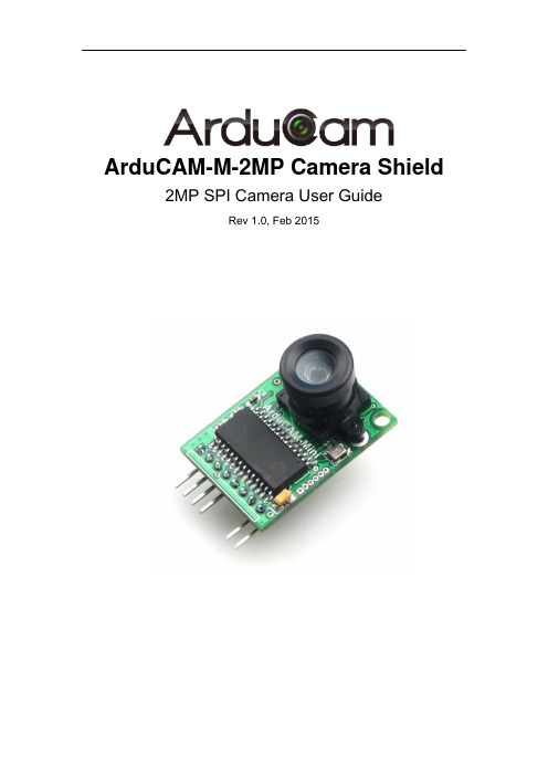
ArduCAM-M-2MP Camera Shield 2MP SPI Camera User GuideRev 1.0, Feb 2015ArduCAM-M-2MP Camera User GuideTable of Contents1 Introduction (2)2 Application (2)3 Features (3)4 Key Specifications (3)5 Pin Definition (3)6 Block Diagram (4)7 Functions (4)7.1 Single Capture Mode (4)7.2 Multiple Capture Mode (4)7.3 JPEG Compression (4)7.4 Normal Read and Burst Read Operation (4)7.5 Rewind Read Operation (5)7.6 Low Power Mode (5)7.7 Image Sensor Control (5)8 Lens Options (6)9 Mechanical Dimension (7)10 Order Information (7)1IntroductionArduCAM-M-2MP is optimized version of ArduCAM shield Rev.C, and is a high definition 2MP SPI camera, which reduce the complexity of the camera control interface. It integrates 2MP CMOS image sensor OV2640, and provides miniature size, as well as the easy to use hardware interface and open source code library. The ArduCAM mini can be used in any platforms like Arduino, Raspberry Pi, Maple, Chipkit, Beaglebone black, as long as they have SPI and I2C interface and can be well mated with standard Arduino boards. ArduCAM mini not only offers the capability to add a camera interface which doesn’t have in some low cost microcontrollers, but also provides the capability to add multiple cameras to a single microcontroller.Figure 1 ArduCAM Mini Shield2ApplicationIoT camerasRobot camerasWildlife camerasOther battery-powered productsCan be used in MCU, Raspberry Pi, ARM, DSP, FPGA platforms3Features2MP image sensor OV2640M12 mount or CS mount lens holder with changeable lens optionsIR sensitive with proper lens combinationI2C interface for the sensor configurationSPI interface for camera commands and data streamAll IO ports are 5V/3.3V tolerantSupport JPEG compression mode, single and multiple shoot mode, one time capture multiple read operation, burst read operation, low power mode and etc.Well mated with standard Arduino boardsProvide open source code library for Arduino, STM32, Chipkit, Raspberry Pi, BeagleBone BlackSmall form of factor4Key Specifications⏹Power supplyNormal :5V/70mALow power mode: 5V/20mA ⏹Active array size: 1600x1200 ⏹Shutter: rolling shutter⏹Lens: 1/4 inch⏹SPI speed: 8MHz ⏹Resolution support:⏹Frame buffer: 384KB UXGA, SVGA,VGA,QVGA,CIF,QCIF ⏹Size: 34 x 24 mm ⏹Format support: RAW, YUV, RGB, JPEG ⏹Weight: 20g ⏹Pixel Size: 2.2µm x 2.2µm⏹Temperature: -10℃~+55℃5Pin DefinitionTable 1 ArduCAM-M-2MP Pin DefinitionPin No. PIN NAME TYPE DESCRIPTION1 CS Input SPI slave chip select input2 MOSI Input SPI master output slave input3 MISO Output SPI master input slave output4 SCLK Input SPI serial clock5 GND GroundPowerground6 +5V POWER 5V Power supply7 SDA Bi-directional Two-Wire Serial Interface Data I/O8 SCL Input Two-Wire Serial Interface Clock6Block DiagramFigure 2 shows the block diagram of ArduCAM mini shield which is composed by lens, image sensor and an ArduChip. The lens is changeable and can be mounted by S-mount (M12x0.5) or CS-mount lens holder. The image sensor is 2MP CMOS OV2640 from Omnivision. The ArduChip uses ArduCAM proprietary third generation camera controller technology which handles the complex camera, memory and user interface hardware timing and provides a user friendly SPI interface.Figure 2 ArduCAM Mini Shield Block Diagram7Functions7.1Single Capture ModeSingle capture mode is the default capture mode of the camera. After issuing a capture command via SPI port, the ArduCAM will wait for a new frame and buffer the one entire image data to the frame buffer, and then assert the completion flag bit in the register. User only needs to poll the flag bit from the register to check out if the capture is done.7.2Multiple Capture ModeMultiple capture mode is advanced capture mode. By setting the number of frames in the capture register, the ArduCAM will capture consequent frames after issuing capture command. Note that number of frames should be set properly and make sure do not exceed the maximum memory space.7.3JPEG CompressionThe JPEG compression function is implemented in the image sensor. With proper register settings to the sensor, user can get different resolution with JPEG image stream output. It is recommended to use JPEG output to get higher resolution than RGB mode, due to the limitation of frame buffer.7.4Normal Read and Burst Read OperationNormal read operation reads each image data by sending a read command in one SPI read operation cycle. While burst read operation only need to send a read command then read multiple image data in one SPI read operation cycle. It is recommended to use burst read operation to get better throughput performance.7.5Rewind Read OperationSometimes user wants to read the same frame of image data multiple times for processing, the rewind read operation is designed for this purpose. By resetting the read pointer to the beginning of the image data, user can read the same image data from the start point again.7.6Low Power ModeSome battery power device need save power when in the idle status, the ArduCAM offers the low power mode to reduce power consumption, by shutdown the sensor and memory circuits.7.7Image Sensor ControlImage sensor control function is implemented in the image sensor. By setting proper set of register settings, user can control the exposure, white balance, brightness, contrast, color saturation and etc.More technical information about ArduCAM mini shield, please read ArduCAM-M-2MP Hardware Application Note.pdf and ArduCAM-M-2MP Software Application Note.pdf for detail.8Lens OptionsThe ArduCAM-M-2MP camera shield is shipped with default LS-4011 (S mount) or LS-6018 (CS mount), lenses specification list as follows. S mount lenses normally have build IR cut filter, while the CS mount lenses doesn’t have build in IR cut filter.Please contact us ***************** for more lens options.LS-4011 Lens SpecificationFigure 3 S Mount Lens SpecificationLS-6018 Lens SpecificationFigure 4 CS Mount Lens Specification9Mechanical Dimension10Order InformationPart Number DescriptionPreinstalled Pin Header ArduCAM-M-2MP-SM01 SMountArduCAM-M-2MP-SM02 S Mount Without Preinstalled Pin HeaderArduCAM-M-2MP-CSM01 CS Mount Preinstalled Pin HeaderArduCAM-M-2MP-CSM02 CS Mount Without Preinstalled Pin Header。
30万像素摄像头模块
30万像素摄像头模块本文将介绍30万像素摄像头模块的基本信息和用途。
基本信息分辨率:30万像素接口类型:XXXX图像传感器:XXXX外形尺寸:XXXX工作电压:XXXX用途30万像素摄像头模块在以下应用领域具有广泛的用途:安防监控系统:可用于监控场所、追踪行为和记录事件。
无人机:可用于无人机的航拍和视频传输。
视频通话:适用于网络视频通话、会议和远程教育等领域。
工业视觉:可用于检测和识别、自动化生产等工业领域。
智能家居:可用于家庭监控、智能门铃等智能家居设备。
请注意:以上用途仅为举例,实际应用领域可能更多且广泛。
以上是对30万像素摄像头模块的基本介绍和用途说明,希望对您有所帮助。
高像素:采用30万像素摄像头,可以捕捉清晰细腻的图像。
易于安装:摄像头模块设计紧凑,便于安装在各种设备上。
基于USB接口:摄像头模块采用USB接口连接,方便快捷。
高性能图像处理:配备先进的图像处理芯片,能够实现高质量的图像处理和增强功能。
宽视角:摄像头模块具有宽视角,可以覆盖更广阔的场景。
兼容性强:摄像头模块兼容各种操作系统,包括Windows、Mac和Linux等。
多种应用领域:适用于视频会议、监控系统、机器视觉等多种应用领域。
该30万像素摄像头模块具有以下功能:实时图像采集:可以实时采集图像,传输到计算设备进行处理。
高清视频录制:支持高清视频录制,录制出清晰细腻的视频。
面部识别:具备面部识别功能,可以用于人脸识别、表情分析等应用。
动态追踪:支持动态追踪功能,能够跟踪并自动对焦移动对象。
声音采集:支持声音采集,可以进行音频录制或语音识别应用。
多种分辨率选择:可以根据需要选择不同的分辨率,满足不同应用场景的需求。
以上是关于30万像素摄像头模块的特点和功能描述。
该摄像头模块具有高像素、易于安装、高性能图像处理等特点,广泛适用于多种应用领域。
同时,它具备实时图像采集、高清视频录制、面部识别等功能,能够满足不同需求的应用场景。
30万像素摄像头模块是一种具有较高像素分辨率的摄像头设备,广泛应用于多个领域。
手机摄像模组基本知识讲解

UV固化 功能FQC 外观FQC OQC 贴膜 OQC 包装 OQA出货
炉后QC
2、COB/COF工艺流程
PQC 贴板 烘烤后检查 调焦
分粒
振动
S M T 阶 段
锡膏印刷 印刷QC 贴片 炉前QC来自回流焊 炉后QC百级 组装 阶段 (百 级无 尘车 间)
烘烤 H/M W/B后清洗 W/B后检查 W/B Plasma Clean Snap Cure D/B SMT板清洗 镜头清洁
点螺纹胶
千级 检测 阶段 (千 级无 尘车 间)
UV固化 功能FQC 外观FQC OQC 贴膜 OQC 包装 OQA出货
3、AF模组工艺流程
SMT阶段(流程同上)
SMT板清洗 D/B 功测 调焦 VCM引脚焊接 烘烤后检查 烘烤 Holder清洗 IR贴付 UV照射 VCM组装 画胶 IR清洁 半成品功测 烘烤 烘烤后检查 PQC 振动 分粒 OQA出货 Lens VCM锁配 点螺纹胶 UV固化 功能FQC 外观FQC OQC 贴膜 OQC 包装
Sensor简介
Sensor:图像传感器,又称芯片、晶圆、Wafer。是感光元器件,主要作用 是将光信号转换为电信号。主要分为CCD和CMOS两种。 CMOS Sensor根据其封装 方式可以分为CSP、COB 两种结构。
我们模组的像素划分就是 以Sensor的像素为依据的。
滤光片简介
滤光片:简称IR片,主要组成分三部分,载体(白玻璃)、截止面镀层(IR 面)、增透面镀层(AR面)。 如下图,为手机模组普通IR的光谱图 IR主要作用是透过 人眼可见光波段, 截止非可见光。主 要波长范围是380700nm之间。 IR用会导致模组出 现偏色、杂光、解 析NG等不良现象。
摄像头模块工作原理
摄像头模块工作原理
摄像头模块是一种通过图像传感器将光信号转换为电信号的装置,用于捕捉图像或视频。
其工作原理涉及以下几个步骤:
1. 感光:摄像头模块内部有一个图像传感器,通常是CMOS (互补金属氧化物半导体)或CCD(电荷耦合器件)传感器。
这些传感器能够感知光信号,并将其转换为电荷。
2. 电荷转换:光信号在传感器上生成电荷,并通过一系列的电荷转换和放大步骤进行处理。
传感器上的每个像素都有一个光敏元件和一个电荷转换器,将光信号转换为电信号。
3. 数字化:经过电荷转换之后,模拟电信号将通过模数转换器(ADC)转换为数字信号。
ADC将连续的模拟信号转换为离
散的数字信号,使其能够通过数字处理单元进行处理。
4. 图像处理:一旦信号被数字化,可以对其进行各种图像处理操作,例如调整亮度、对比度、色彩平衡等。
还可以进行数字降噪、图像滤波等算法处理。
5. 数据传输:处理完成的图像数据可以通过不同的接口进行传输,例如USB、HDMI、SPI等。
这些接口可以将图像数据传
输到计算机、显示设备或其他外部设备上。
6. 图像显示:最后,图像数据可以被显示在屏幕上,或者保存为图像文件,以供后续查看或分析。
总之,摄像头模块的工作原理是通过感光器件将光信号转换为电信号,经过模数转换和数字处理后,传输图像数据并进行显示。
摄像头模组的介绍
摄像头模组的介绍摄像头模组(Camera Module)是一种集成了摄像头传感器、图像处理器和相关接口电路的模块化设备。
它被广泛应用于各种电子设备中,如智能手机、平板电脑、数码相机、医疗设备、工业视觉系统等。
摄像头模组的出现极大地促进了图像采集和图像处理技术的发展,使得用户可以方便地使用高质量的图像和视频功能。
图像处理器是摄像头模组中的核心部件,负责对传感器采集的图像数据进行处理和优化。
图像处理器可以对图像进行去噪、增强、校正、压缩等操作,使得用户获得更加清晰、真实的图像。
同时,图像处理器还可以支持实时视频流传输、自动对焦、人脸识别、智能场景识别等功能。
不同的图像处理器技术和算法可以提供不同的图像效果和功能。
摄像头模组还包含了与设备连接和通信的接口电路,如MIPI (Mobile Industry Processor Interface)接口、USB(Universal Serial Bus)接口、I2C(Inter-Integrated Circuit)接口等。
这些接口可以与主设备进行数据传输和控制命令的交互,实现图像采集和处理的各项功能。
摄像头模组的选型和设计需要考虑多方面的因素。
首先是摄像头传感器的像素与尺寸要求,高像素的传感器可以提供更高分辨率的图像,但也会增加成本和功耗。
其次是图像处理器的性能与功能要求,不同的应用场景可能需要不同的图像处理算法和功能模块。
此外,摄像头模组的连接接口和尺寸也需要与主设备相匹配,以保证良好的兼容性和稳定性。
摄像头模组的市场需求和应用领域不断扩大。
随着智能手机和平板电脑的普及,对高质量图像和视频的需求越来越大,摄像头模组市场得到快速发展。
与此同时,工业视觉、医疗设备、安防监控等领域也对摄像头模组的高清晰度、低功耗、稳定性等提出了更高要求。
因此,摄像头模组制造商不断提升产品技术和性能,以满足市场需求。
总的来说,摄像头模组是一种集成了摄像头传感器、图像处理器和相关接口电路的模块化设备,广泛用于智能手机、平板电脑、数码相机、医疗设备、工业视觉系统等领域。
- 1、下载文档前请自行甄别文档内容的完整性,平台不提供额外的编辑、内容补充、找答案等附加服务。
- 2、"仅部分预览"的文档,不可在线预览部分如存在完整性等问题,可反馈申请退款(可完整预览的文档不适用该条件!)。
- 3、如文档侵犯您的权益,请联系客服反馈,我们会尽快为您处理(人工客服工作时间:9:00-18:30)。
带RS232串行接口的串口摄像头模块
规格参数
特性参数
图像传感器类型CMOS CMOS 1/4英寸
象素尺寸 5.6um*5.6um 白平衡自动
暴光自动
增益自动
快门电子旋转快门(ERS)
图像像素40万像素信噪比45DB
动态范围60DB
最大模拟
增益
16DB
帧频640*480 30fps
扫描模式逐行扫描
可视角度90度(可选)
图像大小640*480 320*240 160*120
串口速率最大115200 工作电流75MA
工作电流
(红外灯工
作)
250MA
工作电压DC +5 伏(+/-5%)
工作环境
温度
-20 ~ +60℃
工作湿度20% - 80%PH
图像接口工业RS232
模组型号:RS232串口摄像头
1模组简介
RS232串口摄像头是我公司推出的新一代串口摄像头模组,具有串口抓拍高清晰图像的功能。
串口摄像头模组是通过串口获取JPG图像的模块,可以很容易集成到设备中去,让设备具有图像抓拍功能。
2性能描述
1.VGA/QVGA/160*120 分辨率。
2.支持串口读取JPG图像。
3.上电默认串口波特率38400。
4.直流3.3V 或者5V 供电。
5.尺寸大小32mm×32mm。
包括镜头厚度2.5cm
6.摄像头工作电流为80-100MA。
3适用领域
▲各种图像采集系统
▲环境监控
▲工业现场控制
▲医疗设备
▲可视电话
▲安全防盗
▲车载GPS
4尺寸图
5接口定义及联线说明(以前是用焊线的,现在已不焊线,用户自行连接)序项目描述
红色+5V 电源供电
黑色GND 电源地
白色TXD(OUT)联到CPU 或PC 的RXD 端
黄色RXD(IN)联到CPU 或PC 的TXD 端
6通讯协议
1.复位返回
56 00 26 00 76 00 26 00
2.拍照返回
56 00 36 01 00 76 00 36 00 00
3.读长度返回
56 00 34 01 00 76 00 34 00 04 00 00 XH XL
XH XL JPEG 文件长度,高位字节在前,低位字节在后
4.读数
56 00 32 0C 00 0A 00 00 MH ML 00 00 KH KL XX XX
返回
76 00 32 00 00 (间隔时间)FF D8 。
……。
(间隔时间)76 00 32 00 00 (间隔时间)= XX XX*0.01 毫秒XX XX 建议为00 0A
00 00 MH ML 启始地址
00 00 KH KL 数据长度
先高位字节,后低位字节
5.停止拍照返回
56 00 36 01 03 76 00 36 00 00
6. 压缩率返回
56 00 31 05 01 01 12 04 XX 76 00 31 00 00 XX 一般选36 XX 从0X00 到0XFF
7.图像大小返回
56 00 31 05 04 01 00 19 11 (320*240)76 00 31 00 00 56 00 31 05 04 01 00 19 00 (640*480)76 00 31 00 00
设置后要送复位命令或重新上电
8.省电返回
56 00 3E 03 00 01 01 76 00 3E 00 00
退出省电返回
56 00 3E 03 00 01 00 76 00 3E 00 00
9.修改串口速率
56 00 24 03 01 XX XX 76 00 24 00 00
XX XX 速率
AE C8 9600
56 E4 19200
2A F2 38400
1C 4C 57600
0D A6 115200
备注:
1.每次读数的起始地址必须是8 的倍数
2.对于多个摄像头时56 XX 36 01 00 XX 是设备号
3.图像压缩摄像机里有MAX232IC,如同CPU 直接联,需去掉MAX232IC,建议CPU 端加个MAX232IC,因为如用TTL 电平,图像压缩摄像机同CPU 的距里不超过1 米。
4.摄像头工作电流为80-100MA,因为串口摄像头是被动工作,因此建议用可控的开关对串口摄像头的电源控制。
5. 上电后,串口摄像头会主动送
Ctrl infr exist
User-defined sensor
625
Init end
你只判断收到Init end(36 32 35 0D 0A 49 6E 69 74 20 65 6E 64 0D 0A )就可以,然后等2-3 秒就送拍照命令,就可以了
这是摄像头上电过程
这是读取一张JPEG图像的过程
这是我们提供的摄像头上位机测试程序,可以通过串口连接,进行拍照。
这是单片机的C参考程序,以前用AVR时用过的,不过主要是串口通信部分,用其它单片机的话,改一下也就可以了。
摄像头上电
Iint end (36 32 35 0D 0A 49 6E69
74 20 65 6E 64 0D 0A ) ?
延时2-3秒后开始拍照延时。