数字集成电路第二版答案
数字集成电路习题答案PPT课件

(2) pmos :
VGT VGS VT 0 0.5 0.4 0.1 VDS
pmos处于饱和区,Vmin 0.1v
ID
kn'
(W L
)(VGTVmin
Vm2in 2
)(1 VDS )
30 (0.1 0.05) 0.1 (1 0.11.25)
0.169A
3.简述MOS管的电容分布,及其模型
的最小尺寸为(W=0.375m,L=0.25m,即W/L=0.375/0.25)
求出g,VIL,VIH,NML,NMH
NMOS PMOS
VT0(V) 0.43 -0.4
(V0.5) 0.4 -0.4
VDSAT(V) 0.63 -1
k’(A/V2) 115×10-6 -30×10-6
(V-1) 0.06 -0.1
CP D Q Q′
写在最后
经常不断地学习,你就什么都知道。你知道得越多,你就越有力量 Study Constantly, And You Will Know Everything. The More
You Know, The More Powerful You Will Be
Thank You
(5R R3)C R3 4R
8
DB Ck RBk k 1 R1C1 R1C2 (R1 R3 )C3 R1C4 (R1 R3 )C5 (R1 R3 R6 )C6 (R1 R3 )C7 (R1 R3 R6 R8 )C8 0.25* 250 0.25*750 (0.25 0.5) * 250 0.25* 250 (0.25 0.5) *1000 (0.25 0.5 1) * 250 (0.25 0.5) *500 (0.25 0.5 11000) * 250 62.5 187.5 187.5 62.5 750 437.5 375 250437.5 0.2525(ns)
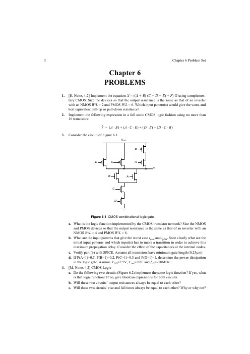
数字集成电路--电路、系统与设计(第二版)课后练习题第六.
数字集成电路--电路、系统与设计(第⼆版)课后练习题第六.Digital Integrated Circuits - 2nd Ed 11 DESIGN PROJECT Design, lay out, and simulate a CMOS four-input XOR gate in the standard 0.25 micron CMOS process. You can choose any logic circuit style, and you are free to choose how many stages of logic to use: you could use one large logic gate or a combination of smaller logic gates. The supply voltage is set at 2.5 V! Your circuit must drive an external 20 fF load in addition to whatever internal parasitics are present in your circuit. The primary design objective is to minimize the propagation delay of the worst-case transition for your circuit. The secondary objective is to minimize the area of the layout. At the very worst, your design must have a propagation delay of no more than 0.5 ns and occupy an area of no more than 500 square microns, but the faster and smaller your circuit, the better. Be aware that, when using dynamic logic, the precharge time should be made part of the delay. The design will be graded on themagnitude of A × tp2, the product of the area of your design and the square of the delay for the worst-case transition.。
数字集成电路-电路系统与设计第二版课程设计
数字集成电路-电路系统与设计第二版课程设计
一、课程设计介绍
数字集成电路是现代电路设计中的重要组成部分,也是计算机科学与工程的重要分支。
本课程设计旨在通过对数字集成电路的系统与设计进行探究,并结合具体的案例来设计和实现数字集成电路,使学生能够熟悉数字集成电路的基本原理、设计方法和实现技术。
本课程设计主要包含以下内容:
1.数值系统和编码
2.逻辑功能设计:组合逻辑电路和时序逻辑电路
3.集成电路设计方法和流程
4.VHDL和FPGA实现数字逻辑电路
5.数字信号处理器
通过本次课程设计,学生将掌握数字集成电路的系统性设计思路和实现方法,具备数字电路设计的基本能力和实际操作技术,能够针对具体应用场景提出解决方案,实现数字电路的设计、验证和调试。
二、课程设计要求
1. 课程设计题目
本次课程设计的题目为“4位计数器设计”。
2. 软件工具
VHDL编程软件和EDA工具
1。
【精品】数字集成电路电路、系统与设计第二版课后练习题第六章CMOS组合逻辑门的设计
【精品】数字集成电路--电路、系统与设计(第二版)课后练习题第六章CMOS组合逻辑门的设计第六章 CMOS组合逻辑门的设计1.为什么CMOS电路逻辑门的输入端和输出端都要连接到电源电压?CMOS电路采用了MOSFET(金属氧化物半导体场效应管)作为开关元件,其中N沟道MOSFET(NMOS)和P沟道MOSFET(PMOS)分别用于实现逻辑门的输入和输出。
NMOS和PMOS都需要连接到电源电压,以使其能够正常工作。
输入端连接到电源电压可以确保信号在逻辑门中正常传递,输出端连接到电源电压可以确保输出信号的正确性和稳定性。
2.为什么在CMOS逻辑门中要使用两个互补的MOSFET?CMOS逻辑门中使用两个互补的MOSFET是为了实现高度抗干扰的逻辑功能。
其中,NMOS和PMOS分别用于实现逻辑门的输入和输出。
NMOS和PMOS的工作原理互补,即当NMOS导通时,PMOS截止,当PMOS导通时,NMOS截止。
这样的设计可以在逻辑门的输出上提供高电平和低电平的稳定性,从而提高逻辑门的抗干扰能力。
3.CMOS逻辑门的输入电压范围是多少?CMOS逻辑门的输入电压范围通常是在0V至电源电压之间,即在低电平和高电平之间。
在CMOS逻辑门中,低电平通常定义为输入电压小于0.3Vdd(电源电压的30%),而高电平通常定义为输入电压大于0.7Vdd(电源电压的70%)。
4.如何设计一个基本的CMOS逻辑门?一个基本的CMOS逻辑门可以由一个NMOS和一个PMOS组成。
其中,NMOS的源极连接到地,栅极连接到逻辑门的输入,漏极连接到PMOS的漏极;PMOS的源极连接到电源电压,栅极连接到逻辑门的输入,漏极连接到输出。
这样的设计可以实现逻辑门的基本功能。
5.如何提高CMOS逻辑门的速度?可以采取以下方法来提高CMOS逻辑门的速度:•减小晶体管的尺寸:缩小晶体管的尺寸可以减小晶体管的电容和电阻,从而提高逻辑门的响应速度。
•优化电源电压:增加电源电压可以提高晶体管的驱动能力,从而加快逻辑门的开关速度。
电子技术(数字部分)第二版课后习题参考答案
& 1
& 1
& Y
B
C
1.12 用代数法化简下列各式
(1)AB BC A(
)
(2)(A B AB
(3)ABC B C( ) (5)AB AB AB AB
)
4 ABABCABAB (
)
(6)(A B
) (A B) (AB AB)()
7
(7)B ABC AC AB BC
(8)ABC ABC ABC A
8
(
1)
() (1 C B
ABCD ABD BC D ABD DC BC BD ABD C BC BD ()
ABD ABC BC BD BD DA BC CA BD BA BC BA ()
AB BC BD
(10) AC ABC BC ABC AC ABC BC ABC (A C A B C BC ABC AB AC CA CB C BC ABC)(
2-4 ) :
(l)43 (2)127 (3 ) 254.25 (4 ) 2.718
解:(1)
2 43 1 2 21 1 2 10 0
25 1 22 0 21 1
0
43=(101011)B (101 011)B=(53)O (0010 1011)B=(2B)H
(2)
2 127 1 2 63 1 2 31 1 2 15 1
10
通止止通通止止通通止 0
11
通止通止通止通止止通 1
同或 L AB AB A B
2.4 试分析图题 2.4 所示的 CMOS 电路,说明它们的逻辑功能。
解:
EN 1 EN 0 L 高阻 L A ( )a
EN=1,TN2、TP2 截止,电路不工作,L=高阻;EN=0,TN2、TP2 导通,TN1、TP1 为反相
数字集成电路--电路、系统与设计(第二版)课后练习题-第四章 导线-Chapter 4 The Wire

1Chapter 4 Problem SetChapter 4Problems1.[M, None, 4.x] Figure 0.1 shows a clock-distribution network. Each segment of the clock net-work (between the nodes) is 5 mm long, 3 μm wide, and is implemented in polysilicon. Ateach of the terminal nodes (such as R ) resides a load capacitance of 100 fF.a.Determine the average current of the clock driver, given a voltage swing on the clock linesof 5 V and a maximum delay of 5 nsec between clock source and destination node R . Forthis part, you may ignore the resistance and inductance of the networkb.Unfortunately the resistance of the polysilicon cannot be ignored. Assume that eachstraight segment of the network can be modeled as a Π-network. Draw the equivalent cir-cuit and annotate the values of resistors and capacitors.c.Determine the dominant time-constant of the clock response at node R .2.[C, SPICE, 4.x] You are designing a clock distribution network in which it is critical to mini-mize skew between local clocks (CLK 1, CLK 2, and CLK 3). You have extracted the RC net-work of F igure 0.2, which models the routing parasitics of your clock line. Initially, you notice that the path to CLK 3 is shorter than to CLK 1 or CLK 2. In order to compensate for this imbalance, you insert a transmission gate in the path of CLK 3 to eliminate the skew.a.Write expressions for the time-constants associated with nodes CLK 1,CLK 2 and CLK 3.Assume the transmission gate can be modeled as a resistance R 3.b.If R 1 = R 2 = R 4 = R 5 = R and C 1 = C 2 = C 3 = C 4 = C 5 = C , what value of R 3 is required to balance the delays to CLK 1, CLK 2, and CLK 3?c.For R =750Ω and C =200fF, what (W /L )’s are required in the transmission gate to elimi-nate skew? Determine the value of the propagation delay.d.Simulate the network using SPICE, and compare the obtained results with the manually obtained numbers.3.[M, None, 4.x]Consider a CMOS inverter followed by a wire of length L . Assume that in thereference design, inverter and wire contribute equally to the total propagation delay t pref . Youmay assume that the transistors are velocity-saturated. The wire is scaled in line with the idealwire scaling model . Assume initially that the wire is a local wire .a.Determine the new (total) propagation delay as a a function of t p ref , assuming that technol-ogy and supply voltage scale with a factor 2. Consider only first-order effects.b.Perform the same analysis, assuming now that the wire scales a global wire , and the wire length scales inversely proportional to the technology.Figure 0.1Clock-distribution network.SR2Chapter 4 Problem Setc.Repeat b, but assume now that the wire is scaled along the constant resistance model. You may ignore the effect of the fringing capacitance.d.Repeat b, but assume that the new technology uses a better wiring material that reduces the resistivity by half, and a dielectric with a 25% smaller permittivity.e.Discuss the energy dissipation of part a. as a function of the energy dissipation of the orig-inal design E ref .f.Determine for each of the statements below if it is true, false, or undefined, and explain in one line your answer. - When driving a small fan-out, increasing the driver transistor sizes raises the short-circuit power dissipation. - Reducing the supply voltage, while keeping the threshold voltage constant decreases the short-circuit power dissipation.- Moving to Copper wires on a chip will enable us to build faster adders.- Making a wire wider helps to reduce its RC delay.- Going to dielectrics with a lower permittivity will make RC wire delay more impor-tant.4.[M, None, 4.x] A two-stage buffer is used to drive a metal wire of 1 cm. The first inverter is of minimum size with an input capacitance Ci=10 fF and an internal propagation delay t p0=50 ps and load dependent delay of 5ps/fF. The width of the metal wire is 3.6 μm. The sheet resis-tance of the metal is 0.08 Ω/, the capacitance value is 0.03 fF/μm 2and the fringing field capacitance is 0.04fF/μm.a.What is the propagation delay of the metal wire?pute the optimal size of the second inverter. What is the minimum delay through the buffer?c.If the input to the first inverter has 25% chance of making a 0-to-1 transition, and the whole chip is running at 20MHz with a 2.5 supply voltage, then what’s the power con-sumed by the metal wire?5.[M, None, 4.x]To connect a processor to an external memory an off -chip connection is neces-sary. The copper wire on the board is 15 cm long and acts as a transmission line with a charac-teristic impedance of 100Ω.(See F igure 0.3). The memory input pins present a very highimpedance which can be considered infinite. The bus driver is a CMOS inverter consisting ofvery large devices: (50/0.25) for the NMOS and (150/0.25) for the PMOS, where all sizes areClock CLK 1CLK 2CLK 3R 1R 2R 5R 4R 3Model as:Figure 0.2RC clock-distribution network.driver C 1C 3C 4C 5C 2Digital Integrated Circuits - 2nd Ed3 in μm. The minimum size device, (0.25/0.25) for NMOS and (0.75/0.25) for PMOS, has theon resistance 35 kΩ.a.Determine the time it takes for a change in the signal to propagate from source to destina-tion (time of flight). The wire inductance per unit length equals 75*10-8 H/m.b.Determine how long it will take the output signal to stay within 10% of its final value. Youcan model the driver as a voltage source with the driving device acting as a series resis-tance. Assume a supply and step voltage of 2.5V. Hint: draw the lattice diagram for thetransmission line.c.Resize the dimensions of the driver to minimize the total delay.L=15cmMemoryZ=100ΩFigure 0.3The driver, the connecting copper wire and thememory block being accessed.6.[M, None, 4.x] A two stage buffer is used to drive a metal wire of 1 cm. The first inverter is aminimum size with an input capacitance C i=10 fF and a propagation delay t p0=175 ps whenloaded with an identical gate. The width of the metal wire is 3.6 μm. The sheet resistance ofthe metal is 0.08 Ω/, the capacitance value is 0.03 fF/μm2 and the fringing field capacitanceis 0.04 fF/μm.a.What is the propagation delay of the metal wire?pute the optimal size of the second inverter. What is the minimum delay through thebuffer?7.[M, None, 4.x] For the RC tree given in Figure 0.4 calculate the Elmore delay from node A tonode B using the values for the resistors and capacitors given in the below in Table 0.1.Figure 0.4RC tree for calculating the delay4Chapter 4 Problem SetTable 0.1Values of the components in the RC tree of Figure 0.4Resistor Value(Ω)Capacitor Value(fF)R10.25C1250R20.25C2750R30.50C3250R4100C4250R50.25C51000R6 1.00C6250R70.75C7500R81000C82508.[M, SPICE, 4.x] In this problem the various wire models and their respective accuracies willbe studied.pute the 0%-50% delay of a 500um x 0.5um wire with resistance of 0.08 Ω/,witharea capacitance of 30aF/um2, and fringing capacitance of 40aF/um. Assume the driverhas a 100Ω resistance and negligible output capacitance.•Using a lumped model for the wire.•Using a PI model for the wire, and the Elmore equations to find tau. (see Chapter 4, figure4.26).•Using the distributed RC line equations from Chapter 4, section 4.4.4.pare your results in part a. using spice (be sure to include the source resistance). Foreach simulation, measure the 0%-50% time for the output•First, simulate a step input to a lumped R-C circuit.•Next, simulate a step input to your wire as a PI model.•Unfortunately, our version of SPICE does not support the distributed RC model as described in your book (Chapter 4, section 4.5.1). Instead, simulate a step input to yourwire using a PI3 distributed RC model.9.[M, None, 4.x] A standard CMOS inverter drives an aluminum wire on the first metal layer.Assume Rn=4kΩ, Rp=6kΩ. Also, assume that the output capacitance of the inverter is negli-gible in comparison with the wire capacitance. The wire is .5um wide, and the resistivity is0.08 Ω/..a.What is the "critical length" of the wire?b.What is the equivalent capacitance of a wire of this length? (For your capacitance calcula-tions, use Table 4.2 of your book , assume there’s field oxide underneath and nothingabove the aluminum wire)Digital Integrated Circuits - 2nd Ed510.[M, None, 4.x] A 10cm long lossless transmission line on a PC board (relative dielectric con-stant = 9, relative permeability = 1) with characteristic impedance of 50Ω is driven by a 2.5Vpulse coming from a source with 150Ω resistance.a.If the load resistance is infinite, determine the time it takes for a change at the source toreach the load (time of flight).Now a 200Ω load is attached at the end of the transmission line.b.What is the voltage at the load at t = 3ns?c.Draw lattice diagram and sketch the voltage at the load as a function of time. Determinehow long does it take for the output to be within 1 percent of its final value.11.[C, SPICE, 4.x] Assume V DD =1.5V . Also, use short-channel transistor models forhand analy-sis.a.The Figure 0.5 shows an output driver feeding a 0.2 pF effective fan-out of CMOS gates through a transmission line. Size the two transistors of the driver to optimize the delay.Sketch waveforms of V S and V L , assuming a square wave input. Label critical voltages and times.b.Size down the transistors by m times (m is to be treated as a parameter). Derive a first order expression for the time it takes for V L to settle down within 10% of its final voltage pare the obtained result with the case where no inductance is associated with the wire.Please draw the waveforms of V L for both cases, and comment.e the transistors as in part a). Suppose C L is changed to 20pF. Sketch waveforms of V S and V L , assuming a square wave input. Label critical voltages and instants.d.Assume now that the transmission line is lossy. Perform Hspice simulation for three cases:R=100 Ω/cm; R=2.5 Ω/cm; R=0.5 Ω/cm. Get the waveforms of V S , V L and the middle point of the line. Discuss the results.12.[M, None, 4.x] Consider an isolated 2mm long and 1μm wide M1(Metal1)wire over a silicon substrate driven by an inverter that has zero resistance and parasitic output capccitance. How will the wire delay change for the following cases? Explain your reasoning in each case.a.If the wire width is doubled.b.If the wire length is halved.c.If the wire thickness is doubled.d.If thickness of the oxide between the M1 and the substrate is doubled.13.[E, None, 4.x] In an ideal scaling model, where all dimensions and voltages scale with a fac-tor of S >1 :L=350nH/m 10cm C=150pF/m inV DDV DD V S V LC L =0.2pF Figure 0.5Transmission line between two inverters6Chapter 4 Problem Seta.How does the delay of an inverter scale?b.If a chip is scaled from one technology to another where all wire dimensions,including thevertical one and spacing, scale with a factor of S, how does the wire delayscale? How doesthe overall operating frequency of a chip scale?c.Repeat b) for the case where everything scales, except the vertical dimension of wires (itstays constant).。
数字集成电路--电路、系统与设计(第二版)复习资料
第一章 数字集成电路介绍第一个晶体管,Bell 实验室,1947第一个集成电路,Jack Kilby ,德州仪器,1958 摩尔定律:1965年,Gordon Moore 预言单个芯片上晶体管的数目每18到24个月翻一番。
(随时间呈指数增长)抽象层次:器件、电路、门、功能模块和系统 抽象即在每一个设计层次上,一个复杂模块的内部细节可以被抽象化并用一个黑匣子或模型来代替。
这一模型含有用来在下一层次上处理这一模块所需要的所有信息。
固定成本(非重复性费用)与销售量无关;设计所花费的时间和人工;受设计复杂性、设计技术难度以及设计人员产出率的影响;对于小批量产品,起主导作用。
可变成本 (重复性费用)与产品的产量成正比;直接用于制造产品的费用;包括产品所用部件的成本、组装费用以及测试费用。
每个集成电路的成本=每个集成电路的可变成本+固定成本/产量。
可变成本=(芯片成本+芯片测试成本+封装成本)/最终测试的成品率。
一个门对噪声的灵敏度是由噪声容限NM L (低电平噪声容限)和NM H (高电平噪声容限)来度量的。
为使一个数字电路能工作,噪声容限应当大于零,并且越大越好。
NM H = V OH - V IH NM L = V IL - V OL 再生性保证一个受干扰的信号在通过若干逻辑级后逐渐收敛回到额定电平中的一个。
一个门的VTC 应当具有一个增益绝对值大于1的过渡区(即不确定区),该过渡区以两个有效的区域为界,合法区域的增益应当小于1。
理想数字门 特性:在过渡区有无限大的增益;门的阈值位于逻辑摆幅的中点;高电平和低电平噪声容限均等于这一摆幅的一半;输入和输出阻抗分别为无穷大和零。
传播延时、上升和下降时间的定义传播延时tp 定义了它对输入端信号变化的响应有多快。
它表示一个信号通过一个门时所经历的延时,定义为输入和输出波形的50%翻转点之间的时间。
上升和下降时间定义为在波形的10%和90%之间。
对于给定的工艺和门的拓扑结构,功耗和延时的乘积一般为一常数。
[数字电子技术及应用(第2版)习题答案第1单元习题答案

自我检测题:一、填空题1-1 (1001010)2 =( 112 )8 =( 4A )16 =( 74 )10 1-2 (37.375)10 =( 100101.011 )2 =( 45.3 )8 =( 25.6 )161-3 (CE)16=( 11001110 )2 =( 316 )8 =( 206 )10 =( 001000000110 )8421BCD 1-4在逻辑代数运算的基本公式中,利用分配律可得A (B +C )= AB+AC ,A +BC = (A+B)(A+C) ,利用反演律可得ABC = C B A ++ ,C B A ++ = C B A 。
1-5在数字电路中,半导体三极管多数主要工作在 截止 区和 饱和 区。
1-6 COMS 逻辑门是 单 极型门电路,而TTL 逻辑门是 双 极型门电路。
1-7 COMS 集成逻辑器件在 功耗 、 抗干扰 方面优于TTL 电路,同时还具有结构相对简单,便于大规模集成、制造费用较低等特点。
1-8 CT74 、 CT74H 、 CT74S 、 CT74LS 四个系列的 TTL 集成电路,其中功耗最小的为 CT74LS ;速度最快的为 CT74S ;综合性能指标最好的为 CT74LS 。
二、选择题1-9指出下列各式中哪个是四变量A、B、C、D的最小项( C )。
A 、ABC B 、A+B+C+D C 、ABCD D 、AC 1-10逻辑项D BC A 的逻辑相邻项为( A )。
A 、ABCD —B 、ABCDC 、AB —CD D 、ABC —D1-11当利用三输入的逻辑或门实现两变量的逻辑或关系时,应将或门的第三个引脚( B )。
A 、接高电平B 、接低电平C 、悬空1-12当输入变量A 、B 全为1时,输出为0,则输入与输出的逻辑关系有可能为( A )。
A 、异或 B 、同或 C 、与 D 、或1-13TTL 门电路输入端悬空时应视为( A )电平,若用万用表测量其电压,读数约为( D )。
数字集成电路:电路系统与设计(第二版)

数字集成电路:电路系统与设计(第二版)简介《数字集成电路:电路系统与设计(第二版)》是一本介绍数字集成电路的基本原理和设计方法的教材。
本书的内容覆盖了数字电路的基础知识、逻辑门电路、组合逻辑电路、时序逻辑电路、存储器和程序控制电路等方面。
通过学习本书,读者可以了解数字集成电路的概念、设计方法和实际应用。
目录1.数字电路基础知识 1.1 数字电路的基本概念 1.2 二进制系统与数制转换 1.3 逻辑运算与布尔代数2.逻辑门电路 2.1 与门、或门、非门 2.2 与非门、或非门、异或门 2.3 多输入门电路的设计方法3.组合逻辑电路 3.1 组合逻辑电路的基本原理 3.2 组合逻辑电路的设计方法 3.3 编码器和译码器4.时序逻辑电路 4.1 时序逻辑电路的基本原理 4.2 同步时序电路的设计方法 4.3 异步时序电路的设计方法5.存储器电路 5.1 存储器的基本概念 5.2 可读写存储器的设计方法 5.3 只读存储器的设计方法6.程序控制电路 6.1 程序控制电路的基本概念 6.2 程序控制电路的设计方法 6.3 微程序控制器的设计方法内容概述1. 数字电路基础知识本章主要介绍数字电路的基本概念,包括数字电路与模拟电路的区别、数字信号的表示方法以及数制转换等内容。
此外,还介绍了数字电路中常用的逻辑运算和布尔代数的基本原理。
2. 逻辑门电路逻辑门电路是数字电路中的基本组成单元,本章主要介绍了与门、或门、非门以及与非门、或非门、异或门等逻辑门的基本原理和组成。
此外,还介绍了多输入门电路的设计方法,以及逻辑门电路在数字电路设计中的应用。
3. 组合逻辑电路组合逻辑电路是由逻辑门电路组成的,本章主要介绍了组合逻辑电路的基本原理和设计方法。
此外,还介绍了编码器和译码器的原理和应用,以及在数字电路设计中的实际应用场景。
4. 时序逻辑电路时序逻辑电路是在组合逻辑电路的基础上引入了时序元件并进行时序控制的电路。
本章主要介绍了时序逻辑电路的基本原理和设计方法,包括同步时序电路和异步时序电路的设计。
《集成电路设计(第2版)》习题答案1-5章
CH3
1. 写出晶体外延的意义,列出三种外延生长方法,并比较各自的优缺点。 意义:用同质材料形成具有不同掺杂种类及浓度而具有不同性能的晶体层。外延方法: 液态生长,气相外延生长,金属有机物气相外延生长 2.写出掩膜在 IC 制造过程中的作用,比较整版掩膜和单片掩膜的区别,列举三种掩膜的制 造方法。P28,29 3.写出光刻的作用,光刻有哪两种曝光方式? 作用: 把掩膜上的图形转换成晶圆上的器 件结构。曝光方式有接触与非接触两种。 4.X 射线制版和直接电子束直写技术替代光刻技术有什么优缺点? X 射线(X-ray)具有比可见光短得多的波长,可用来制作更高分辨率的掩膜版。电子
影响,界面势阱的影响 6. 什么是 MOS 器件的体效应? 由于衬底与源端未连接在一起,而引起的阈值电压的变化叫做体效应。 7. 说明 L、W 对 MOSFET 的速度、功耗、驱动能力的影响。 P70,71 8. MOSFET 按比例收缩后对器件特性有什么影响?
I DS
不变,器件占用面积减少,提高电路集成度,减少功耗
CH1
1. 按规模划分,集成电路的发展已经经历了哪几代?它的发展遵循了一条业界著名的定 律,请说出是什么定律? 晶体管-分立元件-SSI-MSI-LSI-VLSI-ULSI-GSI-SOC。MOORE 定律 2. 什么是无生产线集成电路设计?列出无生产线集成电路设计的特点和环境。 拥有设计人才和技术,但不拥有生产线。特点:电路设计,工艺制造,封装分立运行。 环境:IC 产业生产能力剩余,人们需要更多的功能芯片设计 3. 多项目晶圆(MPW)技术的特点是什么?对发展集成电路设计有什么意义? MPW:把几到几十种工艺上兼容的芯片拼装到一个宏芯片上,然后以步行的方式排列 到一到多个晶圆上。意义:降低成本。 4. 集成电路设计需要哪四个方面的知识? 系统,电路,工具,工艺方面的知识
数字集成电路——电路、系统与设计(第二版)Chapter10_timing
Contamination and Propagation Delays
Settle to a final value
Begin to change
Settle to a final value
Begin to change as the last time D begins to change
Settle to a final value as the last time D settles to a final value
Digital Integrated Circuits A Design Perspective
Chapter10: Timing Issues
EE141
Timing Issues
Timing Issues
10.1 Timing Classification
10.2 Synchronous Design
Datapath Structure with Feedback
- Routing the clock so that only negative skew occurs is not feasible
- Design of a low-skew clock network is essential
10.2.5 Clock Distribution Techniques
10.3 Summary
EE141
Timing Issues
Sequencing Methods
Registers
2-Phase Latches
EE141
Timing Issues
Timing Diagrams
习题册参考答案-《数字电路基础(第二版)习题册》-A05-3097.docx
课题一组合逻辑电路任务 1 逻辑门电路的识别和应用一、填空题1.与逻辑; Y=A ·B2.或逻辑; Y=A+B3.非逻辑; Y=4.与运算;或运算;非运算5.低电平6.输入电压 Vi ;输出电压 Vo7. 3.6V;0.3V8.输出端并;外接电阻 R;线与;线与;电平9.高电平;低电平;高阻态10.CMOS11.非门;非门二、选择题1. A2. C3. C4. D5. C6. A7. B8. B9. B10.A11.B12.B13.A三、简答题1. Y1:Y2:2.真值表逻辑函数式Y=ABC 3.真值表逻辑表达式Y1=ABY2=Y3= A+B逻辑符号4.5.任务 2 组合逻辑电路的分析和设计一、填空题1.高电平;低电平2.输入逻辑变量的各种可能取值;相应的函数值排列在一起3.逻辑变量;与;或;非4.两输入信号;异或门电路5.代数;卡诺图6.A+B+C ;A;A7.( 1) n; n;(2)原变量;反变量;一;一8.与或式; 1; 09.组合逻辑电路;组合电路;时序逻辑电路;时序电路10.该时刻的输入信号;先前的状态二、选择题1. D2. C3. C4. A5. A三、判断题1.×2.√3.√4.√5.×6.√7.×四、简答题1.略2.( 1) Y=A+ B(2)Y=AB + A B(3)Y=ABC+A + B +C+D=A + B +C+D3. (1)Y=A B C+ABC+ABC+ABC= A C+AC(2) Y= A CD+A B D + D+ACDAB(3)Y=C+ AB+AB4.状态表逻辑功能:相同出1,不同出 0逻辑图5.( a)逻辑函数式Y=AB+ A B真值表逻辑功能:相同出1,不同出 0(b)逻辑函数式 Y=AB+BC+AC真值表逻辑功能:少数服从多数电路,即三人表决器。
6.Y=A ABC +B ABC +C ABC判不一致电路,输入不同,输出为1,;输入相同,输出为0。
数字集成电路--电路、系统与设计(第二版)复习资料

第一章 数字集成电路介绍第一个晶体管,Bell 实验室,1947第一个集成电路,Jack Kilby ,德州仪器,1958 摩尔定律:1965年,Gordon Moore 预言单个芯片上晶体管的数目每18到24个月翻一番。
(随时间呈指数增长)抽象层次:器件、电路、门、功能模块和系统 抽象即在每一个设计层次上,一个复杂模块的内部细节可以被抽象化并用一个黑匣子或模型来代替。
这一模型含有用来在下一层次上处理这一模块所需要的所有信息。
固定成本(非重复性费用)与销售量无关;设计所花费的时间和人工;受设计复杂性、设计技术难度以及设计人员产出率的影响;对于小批量产品,起主导作用。
可变成本 (重复性费用)与产品的产量成正比;直接用于制造产品的费用;包括产品所用部件的成本、组装费用以及测试费用。
每个集成电路的成本=每个集成电路的可变成本+固定成本/产量。
可变成本=(芯片成本+芯片测试成本+封装成本)/最终测试的成品率。
一个门对噪声的灵敏度是由噪声容限NM L (低电平噪声容限)和NM H (高电平噪声容限)来度量的。
为使一个数字电路能工作,噪声容限应当大于零,并且越大越好。
NM H = V OH - V IH NM L = V IL - V OL 再生性保证一个受干扰的信号在通过若干逻辑级后逐渐收敛回到额定电平中的一个。
一个门的VTC 应当具有一个增益绝对值大于1的过渡区(即不确定区),该过渡区以两个有效的区域为界,合法区域的增益应当小于1。
理想数字门 特性:在过渡区有无限大的增益;门的阈值位于逻辑摆幅的中点;高电平和低电平噪声容限均等于这一摆幅的一半;输入和输出阻抗分别为无穷大和零。
传播延时、上升和下降时间的定义传播延时tp 定义了它对输入端信号变化的响应有多快。
它表示一个信号通过一个门时所经历的延时,定义为输入和输出波形的50%翻转点之间的时间。
上升和下降时间定义为在波形的10%和90%之间。
对于给定的工艺和门的拓扑结构,功耗和延时的乘积一般为一常数。
数字集成电路--电路、系统与设计(第二版)课后练习题 第五章 CMOS反相器
C H A P T E R5T H E C M O S I N V E R T E R Quantification of integrity,performance,and energy metrics of an inverterOptimization of an inverter design5.1Exercises and Design Problems5.2The Static CMOS Inverter—An IntuitivePerspective5.3Evaluating the Robustness of the CMOSInverter:The Static Behavior5.3.1Switching Threshold5.3.2Noise Margins5.3.3Robustness Revisited5.4Performance of CMOS Inverter:The DynamicBehavior5.4.1Computing the Capacitances5.4.2Propagation Delay:First-OrderAnalysis5.4.3Propagation Delay from a DesignPerspective5.5Power,Energy,and Energy-Delay5.5.1Dynamic Power Consumption5.5.2Static Consumption5.5.3Putting It All Together5.5.4Analyzing Power Consumption UsingSPICE5.6Perspective:Technology Scaling and itsImpact on the Inverter Metrics180Section 5.1Exercises and Design Problems 1815.1Exercises and Design Problems1.[M,SPICE,3.3.2]The layout of a static CMOS inverter is given in Figure 5.1.(λ=0.125µm).a.Determine the sizes of the NMOS and PMOS transistors.b.Plot the VTC (using HSPICE)and derive its parameters (V OH ,V OL ,V M ,V IH ,and V IL ).c.Is the VTC affected when the output of the gates is connected to the inputs of 4similargates?.d.Resize the inverter to achieve a switching threshold of approximately 0.75V .Do not lay-out the new inverter,use HSPICE for your simulations.How are the noise margins affected by this modification?2.Figure 5.2shows a piecewise linear approximation for the VTC.The transition region isapproximated by a straight line with a slope equal to the inverter gain at V M .The intersectionof this line with the V OH and the V OL lines defines V IH and V IL .a.The noise margins of a CMOS inverter are highly dependent on the sizing ratio,r =k p /k n ,of the NMOS and PMOS e HSPICE with V Tn =|V Tp |to determine the valueof r that results in equal noise margins?Give a qualitative explanation.b.Section 5.3.2of the text uses this piecewise linear approximation to derive simplifiedexpressions for NM H and NM L in terms of the inverter gain.The derivation of the gain isbased on the assumption that both the NMOS and the PMOS devices are velocity saturatedat V M .For what range of r is this assumption valid?What is the resulting range of V M ?c.Derive expressions for the inverter gain at V M for the cases when the sizing ratio is justabove and just below the limits of the range where both devices are velocity saturated.What are the operating regions of the NMOS and the PMOS for each case?Consider theeffect of channel-length modulation by using the following expression for the small-signalresistance in the saturation region:r o,sat =1/(λI D ).Figure 5.1CMOS inverter layout.InOutGND V DD =2.5V.Poly Metal1NMOSPMOSPolyMetal12λ182THE CMOS INVERTER Chapter 53.[M,SPICE,3.3.2]Figure 5.3shows an NMOS inverter with resistive load.a.Qualitatively discuss why this circuit behaves as an inverter.b.Find V OH and V OL calculate V IH and V IL .c.Find NM L and NM H ,and plot the VTC using HSPICE.d.Compute the average power dissipation for:(i)V in =0V and (ii)V in =2.5Ve HSPICE to sketch the VTCs for R L =37k,75k,and 150k on a single graph.ment on the relationship between the critical VTC voltages (i.e.,V OL ,V OH ,V IL ,V IH )and the load resistance,R L .g.Do high or low impedance loads seem to produce more ideal inverter characteristics?4.[E,None,3.3.3]For the inverter of Figure 5.3and an output load of 3pF:a.Calculate t plh ,t phl ,and t p .b.Are the rising and falling delays equal?Why or why not?pute the static and dynamic power dissipation assuming the gate is clocked as fast as possible.5.The next figure shows two implementations of MOS inverters.The first inverter uses onlyNMOS transistors.V OH V OL inV outFigure 5.2A different approach to derive V IL and V IH .V outV in M 1W/L =1.5/0.5+2.5VFigure 5.3Resistive-load inverterR L =75k ΩSection 5.1Exercises and Design Problems183a.Calculate V OH ,V OL ,V M for each case.e HSPICE to obtain the two VTCs.You must assume certain values for the source/drain areas and perimeters since there is no layout.For our scalable CMOS process,λ =0.125μm,and the source/drain extensions are 5λfor the PMOS;for the NMOS the source/drain contact regions are 5λx5λ.c.Find V IH ,V IL ,NM L and NM H for each inverter and comment on the results.How can you increase the noise margins and reduce the undefined region?ment on the differences in the VTCs,robustness and regeneration of each inverter.6.Consider the following NMOS inverter.Assume that the bulk terminals of all NMOS deviceare connected to GND.Assume that the input IN has a 0V to 2.5V swing.a.Set up the equation(s)to compute the voltage on node x .Assume γ=0.5.b.What are the modes of operation of device M2?Assume γ=0.c.What is the value on the output node OUT for the case when IN =0V?Assume γ=0.d.Assuming γ=0,derive an expression for the switching threshold (V M )of the inverter.Recall that the switching threshold is the point where V IN =V OUT .Assume that the devicesizes for M1,M2and M3are (W/L)1,(W/L)2,and (W/L)3respectively.What are the limitson the switching threshold?For this,consider two cases:i)(W/L)1>>(W/L)2V DD =2.5V V IN V OUTV DD =2.5V V IN V OUT M 2M 1M 4M 3W/L=0.375/0.25W/L=0.75/0.25W/L=0.375/0.25W/L=0.75/0.25Figure 5.4Inverter ImplementationsV DD =2.5V OUTM1IN M2M3V DD =2.5Vx184THE CMOS INVERTER Chapter 5ii)(W/L)2>>(W/L)17.Consider the circuit in Figure 5.5.Device M1is a standard NMOS device.Device M2has allthe same properties as M1,except that its device threshold voltage is negative and has a valueof -0.4V.Assume that all the current equations and inequality equations (to determine themode of operation)for the depletion device M2are the same as a regular NMOS.Assume thatthe input IN has a 0V to 2.5V swing.a.Device M2has its gate terminal connected to its source terminal.If V IN =0V ,what is the output voltage?In steady state,what is the mode of operation of device M2for this input?pute the output voltage for V IN =2.5V .You may assume that V OUT is small to simplify your calculation.In steady state,what is the mode of operation of device M2for this input?c.Assuming Pr (IN =0)=0.3,what is the static power dissipation of this circuit?8.[M,None,3.3.3]An NMOS transistor is used to charge a large capacitor,as shown in Figure5.6.a.Determine the t pLH of this circuit,assuming an ideal step from 0to 2.5V at the input node.b.Assume that a resistor R S of 5k Ωis used to discharge the capacitance to ground.Deter-mine t pHL .c.Determine how much energy is taken from the supply during the charging of the capacitor.How much of this is dissipated in M1.How much is dissipated in the pull-down resistanceduring discharge?How does this change when R S is reduced to 1k Ω.d.The NMOS transistor is replaced by a PMOS device,sized so that k p is equal to the k n ofthe original NMOS.Will the resulting structure be faster?Explain why or why not.9.The circuit in Figure 5.7is known as the source follower configuration.It achieves a DC levelshift between the input and the output.The value of this shift is determined by the current I 0.Assume x d =0,γ=0.4,2|φf |=0.6V ,V T 0=0.43V ,k n ’=115μA/V 2and λ=0.V DD =2.5VOUTM1(4μm/1μm)IN M2(2μm/1μm),V Tn =-0.4VFigure 5.5A depletion load NMOSinverterV DD =2.5VOutFigure 5.6Circuit diagram with annotated W/L ratios=5pFSection 5.1Exercises and Design Problems 185a.Suppose we want the nominal level shift between V i and V o to be 0.6V in the circuit in Figure 5.7(a).Neglecting the backgate effect,calculate the width of M2to provide this level shift (Hint:first relate V i to V o in terms of I o ).b.Now assume that an ideal current source replaces M2(Figure 5.7(b)).The NMOS transis-tor M1experiences a shift in V T due to the backgate effect.Find V T as a function of V o for V o ranging from 0to 2.5V with 0.5V intervals.Plot V T vs.V oc.Plot V o vs.V i as V o varies from 0to 2.5V with 0.5V intervals.Plot two curves:one neglecting the body effect and one accounting for it.How does the body effect influence the operation of the level converter?d.At V o (with body effect)=2.5V,find V o (ideal)and thus determine the maximum error introduced by the body effect.10.For this problem assume:V DD =2.5V ,W P /L =1.25/0.25,W N /L =0.375/0.25,L =L eff =0.25μm (i.e.x d =0μm),C L =C inv-gate ,k n ’=115μA/V 2,k p ’=-30μA/V 2,V tn0=|V tp0|=0.4V,λ =0V -1, γ=0.4,2|φf |=0.6V ,and t ox =e the HSPICE model parameters for parasitic capacitance given below (i.e.C gd0,C j ,C jsw ),and assume that V SB =0V for all problems except part (e).Figure 5.7NMOS source follower configuration V DD =2.5V V iV oV DD =2.5VV i V oV bias =(a)(b)I o1um/0.25um M1186THE CMOS INVERTER Chapter 5##Parasitic Capacitance Parameters (F/m)##NMOS:CGDO=3.11x10-10,CGSO=3.11x10-10,CJ=2.02x10-3,CJSW=2.75x10-10PMOS:CGDO=2.68x10-10,CGSO=2.68x10-10,CJ=1.93x10-3,CJSW=2.23x10-10a.What is the V m for this inverter?b.What is the effective load capacitance C Leff of this inverter?(include parasitic capacitance,refer to the text for K eq and m .)Hint:You must assume certain values for the source/drain areas and perimeters since there is no layout.For our scalable CMOS process,λ =0.125μm,and the source/drain extensions are 5λfor the PMOS;for the NMOS the source/drain contact regions are 5λx5λ.c.Calculate t PHL ,t PLH assuming the result of (b)is ‘C Leff =6.5fF’.(Assume an ideal step input,i.e.t rise =t fall =0.Do this part by computing the average current used to charge/dis-charge C Leff .)d.Find (W p /W n )such that t PHL =t PLH .e.Suppose we increase the width of the transistors to reduce the t PHL ,t PLH .Do we get a pro-portional decrease in the delay times?Justify your answer.f.Suppose V SB =1V,what is the value of V tn ,V tp ,V m ?How does this qualitatively affect C Leff ?ing Hspice answer the following questions.a.Simulate the circuit in Problem 10and measure t P and the average power for input V in :pulse(0V DD 5n 0.1n 0.1n 9n 20n),as V DD varies from 1V -2.5V with a 0.25V interval.[t P =(t PHL +t PLH )/2].Using this data,plot ‘t P vs.V DD ’,and ‘Power vs.V DD ’.Specify AS,AD,PS,PD in your spice deck,and manually add C L =6.5fF.Set V SB =0Vfor this problem.b.For Vdd equal to 2.5V determine the maximum fan-out of identical inverters this gate candrive before its delay becomes larger than 2ns.c.Simulate the same circuit for a set of ‘pulse’inputs with rise and fall times of t in_rise,fall =1ns,2ns,5ns,10ns,20ns.For each input,measure (1)the rise and fall times t out_rise andV DD =2.5VV IN V OUTC L =C inv-gateL =L P =L N =0.25μmV SB-+(W p /W n =1.25/0.375)Figure 5.8CMOS inverter with capacitiveSection 5.1Exercises and Design Problems 187t out_fall of the inverter output,(2)the total energy lost E total ,and (3)the energy lost due to short circuit current E short .Using this data,prepare a plot of (1)(t out_rise +t out_fall )/2vs.t in_rise,fall ,(2)E total vs.t in_rise,fall ,(3)E short vs.t in_rise,fall and (4)E short /E total vs.t in_rise,fall.d.Provide simple explanations for:(i)Why the slope for (1)is less than 1?(ii)Why E short increases with t in_rise,fall ?(iii)Why E total increases with t in_rise,fall ?12.Consider the low swing driver of Figure 5.9:a.What is the voltage swing on the output node (V out )?Assume γ=0.b.Estimate (i)the energy drawn from the supply and (ii)energy dissipated for a 0V to 2.5V transition at the input.Assume that the rise and fall times at the input are 0.Repeat the analysis for a 2.5V to 0V transition at the input.pute t pLH (i.e.the time to transition from V OL to (V OH +V OL )/2).Assume the input rise time to be 0.V OL is the output voltage with the input at 0V and V OH is the output volt-age with the input at 2.5V .pute V OH taking into account body effect.Assume γ =0.5V 1/2for both NMOS and PMOS.13.Consider the following low swing driver consisting of NMOS devices M1and M2.Assumean NWELL implementation.Assume that the inputs IN and IN have a 0V to 2.5V swing andthat V IN =0V when V IN =2.5V and vice-versa.Also assume that there is no skew between INand IN (i.e.,the inverter delay to derive IN from IN is zero).a.What voltage is the bulk terminal of M2connected to?V in V out V DD =2.5V W L 3μm 0.25μm =p 2.5V0V C L =100fFW L 1.5μm 0.25μm=n Figure 5.9Low Swing DriverV LOW =0.5VOutM1ININ M225μm/0.25μm 25μm/0.25μmC L =1pFFigure 5.10Low Swing Driver188THE CMOS INVERTER Chapter 5b.What is the voltage swing on the output node as the inputs swing from 0V to 2.5V .Showthe low value and the high value.c.Assume that the inputs IN and IN have zero rise and fall times.Assume a zero skewbetween IN and IN.Determine the low to high propagation delay for charging the outputnode measured from the the 50%point of the input to the 50%point of the output.Assumethat the total load capacitance is 1pF,including the transistor parasitics.d.Assume that,instead of the 1pF load,the low swing driver drives a non-linear capacitor,whose capacitance vs.voltage is plotted pute the energy drawn from the lowsupply for charging up the load capacitor.Ignore the parasitic capacitance of the driver cir-cuit itself.14.The inverter below operates with V DD =0.4V and is composed of |V t |=0.5V devices.Thedevices have identical I 0and n.a.Calculate the switching threshold (V M )of this inverter.b.Calculate V IL and V IH of the inverter.15.Sizing a chain of inverters.a.In order to drive a large capacitance (C L =20pF)from a minimum size gate (with inputcapacitance C i =10fF),you decide to introduce a two-staged buffer as shown in Figure5.12.Assume that the propagation delay of a minimum size inverter is 70ps.Also assumeV DD =0.4VV IN V OUTFigure 5.11Inverter in Weak Inversion RegimeSection 5.1Exercises and Design Problems 189that the input capacitance of a gate is proportional to its size.Determine the sizing of thetwo additional buffer stages that will minimize the propagation delay.b.If you could add any number of stages to achieve the minimum delay,how many stages would you insert?What is the propagation delay in this case?c.Describe the advantages and disadvantages of the methods shown in (a)and (b).d.Determine a closed form expression for the power consumption in the circuit.Consider only gate capacitances in your analysis.What is the power consumption for a supply volt-age of 2.5V and an activity factor of 1?16.[M,None,3.3.5]Consider scaling a CMOS technology by S >1.In order to maintain compat-ibility with existing system components,you decide to use constant voltage scaling.a.In traditional constant voltage scaling,transistor widths scale inversely with S,W ∝1/S.To avoid the power increases associated with constant voltage scaling,however,youdecide to change the scaling factor for W .What should this new scaling factor be to main-tain approximately constant power.Assume long-channel devices (i.e.,neglect velocitysaturation).b.How does delay scale under this new methodology?c.Assuming short-channel devices (i.e.,velocity saturation),how would transistor widthshave to scale to maintain the constant power requirement?1InAdded Buffer StageOUTC L =20pF C i =10fF‘1’is the minimum size inverter.??Figure 5.12Buffer insertion for driving large loads.190THE CMOS INVERTER Chapter5DESIGN PROBLEMUsing the0.25μm CMOS introduced in Chapter2,design a static CMOSinverter that meets the following requirements:1.Matched pull-up and pull-down times(i.e.,t pHL=t pLH).2.t p=5nsec(±0.1nsec).The load capacitance connected to the output is equal to4pF.Notice that thiscapacitance is substantially larger than the internal capacitances of the gate.Determine the W and L of the transistors.To reduce the parasitics,useminimal lengths(L=0.25μm)for all transistors.Verify and optimize the designusing SPICE after proposing a first design using manual -pute also the energy consumed per transition.If you have a layout editor(suchas MAGIC)available,perform the physical design,extract the real circuitparameters,and compare the simulated results with the ones obtained earlier.。
1数字电子技术基础 第二版 课后答案 (胡晓光 著) 北京航空航天大学出版社
2.1由TTL门组成的电路如图2.1所示,已知它们的输入短路电流为I is =1.6mA,高电平输入漏电流I iH=40。
试问:当A=B=1时,G1的灌电流(拉,灌)为3.2mA;A=0时,G1的拉电流(拉,灌)为120。
2.2图2.2中示出了某门电路的特性曲线,试据此确定它的下列参数:输出高电平U OH=3V;输出低电平U OL=0.3V;输入短路电流I iS=1.4mA;高电平输入漏电流I iH=0.02mA;阈值电平U T=1.5V;开门电平U ON= 1.5V;关门电平U OFF=1.5V;低电平噪声容限U NL=1.2V;高电平噪声容限U NH=1.5V;最大灌电流I OLmax=15mA;扇出系数N=10.2.3TTL门电路输入端悬空时,应视为高电平;(高电平,低电平,不定)此时如用万用表测量其电压,读数约为1.4V(3.6V,0V,1.4V)。
2.4CT74、CT74H、CT74S、CT74LS四个系列的TTL集成电路,其中功耗最小的为CT74LS;速度最快的为CT74S;综合性能指标最好的为CT74LS。
2.5CMOS门电路的特点:静态功耗极低(很大,极低);而动态功耗随着工作频率的提高而增加(增加,减小,不变);输入电阻很大(很大,很小);噪声容限高(高,低,等)于TTL门。
2.6集电极开路门(OC门)在使用时须在输出与电源之间接一电阻(输出与地,输出与输入,输出与电源)。
2.72.8若G2的悬空的输入端接至0.3V,结果如下表2.9输入悬空时为高电平,M=“0”,V M=0.2V,三态门输出为高阻,M 点电位由后面“与或非”门的输入状态决定,后面与门中有一输入为0,所以V M=0V。
2.102.11上图中门1的输出端断了,门2、3、4为高电平输入,此时V M=1.6V 左右。
2.12不能正常工作,因为不能同时有效,即不能同时为低电平。
2.13图为由TTL“与非”门组成的电路,输入A、B的波形如图所示,试画出V0的波形。
《数字电子技术(第二版)习题册》答案

《数字电⼦技术(第⼆版)习题册》答案数字电⼦技术(第⼆版)》习题册部分参考答案课题⼀认识数字电路任务⼀认识数制与数制转换⼀、填空题1.时间数值1 02.1 8 153.1 128 2554.75.96.16⼆、选择题1.C 2.B 3.C 4.B 5.C 6.A 7.D三、判断题1.V2. V3. X4.X5.V6.X7.V 8.V 9.X四、问答题1.答:数字电路中的信号为⾼电平或低电平两种状态,它正好与⼆进制的 1 和0 相对应,因此,采⽤⼆进制更加⽅便和实⽤。
2.答:⼗六进制具有数据读写⽅便,与⼆进制相互转换简单,较直观地表⽰位状态等优点。
五、计算题1. (1)7 (2)15 (3)31 (4)2132. (1)[1010]2 (2)[1 0000]23)[100 0000 0000]2 (4)[100 0000 0110]23. (1)[650]8 (4)[3153]84. (1)[010 111]2 (2)[001 101 110]23)[010 000 000]2 (4)[001 110 101 101]25. (1)0FH (2)1FH3)36H (4)0AE63H6. (1)0001 0110 B (2)0010 1010 1110 B3)1011 1000 1111 1100B (4)0011 1111 1101 0101B 任务⼆学习⼆进制数算术运算⼀、填空题1.加减乘除2. 0+0=0 0+1=1 1+0=1 1+1=103.0-0=0 1-0=1 1-1=0 10-1=14.0X0=0 0X1=0 1X0=0 1X1=15.1 06.最⾼正负原码7.字节 8.半字节 9.字⼆、选择题1.C 2.B 3.C 4.B 5.B 6.B 7.C3.x4. V四、问答题1.答:将⼆进制数 001 1移位⾄ 0110,是向左移动⼀位,应做乘2运算。
2.答:将⼆进制数 1010 0000 移位⾄ 0001 0100,是向右移动三位,应做除以 8运算。
数字电路逻辑技术(第二版)王毓银课后习题答案
0 0 0 1 0 0
0 0 0 0 1 0
0 0 0 0 0 1
0 0 1
0 1 0
0 1 1
1 0 0
1 0 1
1 1 0
解由真值表可直接写出该编码器的逻辑函数:
{
其逻辑电路如图4.5.21所示
10.用2输入端与非门实现下列逻辑函数(要求器件数最少)
(1)
(2)
解(1)原式=
两次取反,得
(2)
解经化简,得到最简与或式为
上式中 ,给式中加入多余项得
两次取反,得
有2各尾部因子 实现此逻辑共需要3个与非门
(3)
解化简得
两次取反,得
共需要6个与非门实现逻辑
(4)
解化简得
两次取反,得
共需要11个与非门,实现的逻辑图
(5)
解化简得
经检验,由
产生的任意项 无助于减少尾部因子,对最简式直接两次取反,得
解
a b c
Y
F
Z
000
001
010
011
100
101
110
111
1
1
1
0
1
0
0
0
0
1
1
0
1
0
0
1
0
0
0
1
0
1
1
1
(1)据题意3个输入信号a ,b ,c在不同取值组合下的输出Y被列在表2.51中,
故Y的逻辑函数表达式为
Y= (积之和)=
(和之积)
(2)由于当3个输入信号出现奇数1,输出F为1,所以给逻辑功能为奇校验器,其输入a,b,c在不同取值下对应的输出F被列在表2.5.1中,F的逻辑函数表达式为
数字集成电路--电路、系统与设计(第二版)课后练习题 第六章 CMOS组合逻辑门的设计-Chapter 6 Designing
4
Chapter 6 Problem Set
VDD F G
A B
A
A B
A
Figure 6.6 Two-input complex logic gate.
11.
Design and simulate a circuit that generates an optimal differential signal as shown in Figure 6.7. Make sure the rise and fall times are equal.
2
VDD E 6 A A 6 B 6 C 6 D 6 F A B C D 4 4 4 4 E 1 A B C D E 4 4 4 4 E 1 6 F 6 B 6 C 6 D
Chapter 6 Problem SetVDD 6Circ来自it ACircuit B
Figure 6.2 Two static CMOS gates.
Digital Integrated Circuits - 2nd Ed
3
2.5 V
PMOS
M2 W/L = 0.5μm/0.25μm Vout Vin M1 W/L = 4μm/0.25μm NMOS Figure 6.4 Pseudo-NMOS inverter.
a. What is the output voltage if only one input is high? If all four inputs are high? b. What is the average static power consumption if, at any time, each input turns on with an (independent) probability of 0.5? 0.1? c. Compare your analytically obtained results to a SPICE simulation.
lec16

需提供非重叠的时钟信号 否则两管短时同时导通有 竞争产生,使输出不稳定
第七章 时序逻辑电路设计
17
第十六讲 时序逻辑电路设计 Master-Slave Register 主从边沿寄存器
采用两种相反类型的锁存器构成主从边沿触发寄存器。
请问,为什么上图结构为边沿触发寄存器?
请问上图是正沿触发还是负沿触发的寄存器? 答案:正沿触发。 如何构成负沿触发?
Q Clk D Clk Q
15
第七章 时序逻辑电路设计
第十六讲 时序逻辑电路设计 Mux-Based Latch 基于多路开关的锁存器
CLK
Q CLK
D
用传输门构成的正锁 存器,时钟负荷较大
本设计对CLK信号来说 有4个晶体管负载。
CLK
2017/4/27
第七章 时序逻辑电路设计
16
D Q Clk
Clk
Clk
D
Q
2017/4/27
D
Q
第七章 时序逻辑电路设计
8
第十六讲 时序逻辑电路设计 锁存器的类型
2017/4/27
第七章 时序逻辑电路设计
9
第十六讲 时序逻辑电路设计 基于锁存器的设计
• 当 f = 1 时, P 锁存器 处于透明状态。
f
• 当 f = 0 时, N锁存器 处于透明状态。
第十六讲 时序逻辑电路设计 Mux-Based Latch 基于多路开关的锁存器
CLK QM
QM CLK
CLK
对时钟的要求
CLK
仅用 NMOS 也可实现锁存功能,但 会使传送到第一个反相器输入的高 电平下降为VDD-VTn,这对噪声容限 和开关性能都会有影响。同时因反 相器PMOS器件不能完全关断而产 生静态功耗。
- 1、下载文档前请自行甄别文档内容的完整性,平台不提供额外的编辑、内容补充、找答案等附加服务。
- 2、"仅部分预览"的文档,不可在线预览部分如存在完整性等问题,可反馈申请退款(可完整预览的文档不适用该条件!)。
- 3、如文档侵犯您的权益,请联系客服反馈,我们会尽快为您处理(人工客服工作时间:9:00-18:30)。
数字集成电路第二版答案【篇一:《数字集成电路》期末试卷a(含答案)】考试试卷 a姓名学号班级任课教师一、填空题(本大题共10小题,每空格1分,共10分)请在每小题的空格中填上正确答案。
错填、不填均无分。
1.十进制数(68)10对应的二进制数等于;2.描述组合逻辑电路逻辑功能的方法有真值表、逻辑函数、卡诺图、逻辑电路图、波形图和硬件描述语言(hdl)法等,其中描述法是基础且最直接。
3.a?1可以简化为4.图1所示逻辑电路对应的逻辑函数l等于。
abc≥1lcy图1图25.如图2所示,当输入c是(高电平,低电平)时,y?ab。
6.两输入端ttl与非门的输出逻辑函数z?ab,当a=b=1时,输出低电平且vz=0.3v,当该与非门加上负载后,输出电压将(增大,减小)。
7.moore型时序电路和mealy型时序电路相比,型电路的抗干扰能力更强。
8.与同步时序电路相比,异步时序电路的最大缺陷是会产生 9.jk触发器的功能有置0、置1、保持和的ram。
二、选择题(本大题共10小题,每小题2分,共20分)在每小题列出的四个备选项中只有一个是符合题目要求的,请将其代码填写在题后的括号内。
错选、多选或未选均无分。
11.十进制数(172)10对应的8421bcd编码是。
【】a.(1111010)8421bcdb.(10111010)8421bcdc.(000101110010)8421bcd d.(101110010)8421bcd12.逻辑函数z(a,b,c)?ab?ac包含【】a.2 b.3c.4d.513.设标准ttl与非门z?ab的电源电压是+5v,不带负载时输出高电平电压值等于+3.6v,输出低电平电压值等于0.3v。
当输入端a、b电压值va=0.3v,vb=3.6v和va=vb=3.6v两种情况下,输出电压值vz分别为。
a.5v,5v c.3.6v,0.3v【】b.3.6v,3.6v d.0.3v ,3.6v14.图3所示电路的输出逻辑函数z1等于。
a.abcdb.ab+cd d.ab?cd【】c.ab?cd2-4译码器abcdz1z2图3 图415.图4电路是由二进制译码器组成的逻辑电路,输出z2等于。
【】a.ab?abb.ab?ab d.ab?abc. ab?ab16.图5所示所示时序电路中,实现qn?1?qn 的电路是【】acpacpcpb图5cd17.最能直观反映时序电路状态变化关系的是【】a.逻辑电路图 b.时序图 c.状态真值表 d.状态转移图18.可以对脉冲波形整形的电路是()。
【】a.施密特触发器 b.t触发器 c.多谐振荡器 d.译码器19.同样分辨率和时钟脉冲下,并行比较型a/d转换器、逐次逼近型a/d转换器和双积分型a/d转换器中完成一次模数转换时间最长的是转换器。
【】a.双积分型 b.逐次逼近型 c.并行比较型 d.都一样20.某十位d/a转换器满量程输出电压为5.115v,则当输入d=(010*******)2时,输出电压为()伏。
【】 a.5.115v b.1.44vc.2.34v d.0.44v 三、分析题(本大题共6小题,21-26每小题6分,27小题12分,共48分) 21.已知逻辑函数z(a,b,c,d)=∑m(0,2,3,7,8,9)+ ∑d (10,11,12,13,14,15),求逻辑函数z的最简“与或”表达式。
22.分析图6所示电路输出z的最简与或逻辑函数表达式。
abzc图623.图7是用4选1数据选择器设计的一个逻辑电路,试写出输出逻辑函数z的最简与或表达式。
表1 4选1数据选择器功能表c图724.设正边沿d触发器初态为0,试画出图8所示cp和输入信号作用下触发器q端的波形。
cpdq“1“0”图825.移位寄存器cc40194功能如表2所示。
设cc40194初态为q3q2q1q0=0000,电路如图9,试画出十个以上cp脉冲作用下移位寄存器的状态转移图。
1dirq0q1q2q3s0dilcc40194s1cpcpd0d1d2d3rd0rd11图9表2 cc40194功能表26.cmos集成定时器555组成的电路如图10所示,试问:(1)说出电路的名称;(2)画出vc和vo输出电压波形(设输入vi低电平宽度足够窄)。
vi0tvvivotvo00t图1027.已知某同步时序电路如图11所示,试:(1)分析电路的状态转移图,并要求给出详细分析过程。
(2)电路逻辑功能是什么,能否自启动?(3)若计数脉冲fcp频率等于700hz,从q2端输出时的脉冲频率是多少?图11,共22分)28.如图12所示,为一工业用水容器示意图,图中虚线表示水位,a、b、c电极被水浸没时会有信号输出,试用与非门构成的电路来实现下述控制作用:水面在a、b间,为正常状态,亮绿灯g;水面在b、c间或在a以上为异常状态,点亮黄灯y;面在c以下为危险状态,点亮红灯r。
要求写出设计过程。
图1229.某四位二进制加/减计数器的逻辑符号如图13(a)所示,功能表如表3所示。
(1)用该集成计数器和少量与非门计一个8421bcd编码的6进制加法计数器。
(2)分析图13(b)电路的逻辑功能,并画出完整的状态转移图。
1cp1(a)(b)图13【篇二:数字逻辑与数字集成电路习题】t>(计算机科学与技术专业、信息安全专业)2004年7月计算机与信息学院、计算机系统结构教研室1一、选择题1.十进制数33的余3码为。
a. 00110110b. 110110c. 01100110d. 1001002.二进制小数-0.0110的补码表示为。
a.0.1010 b.1.1001c.1.0110 d.1.10103.两输入与非门输出为0时,输入应满足。
a.两个同时为1b.两个同时为0 c.两个互为相反 d.两个中至少有一个为04.某4变量卡诺图中有9个“0”方格7个“1”方格,则相应的标准与或表达式中共有多少个与项?a. 9 b.7c.16 d.不能确定5. 下列逻辑函数中,与f?a相等的是。
(a)f1?a?1 (b)f2?a⊙1 (c)f3?a?1 (d)f4?a?06. 设计一个6进制的同步计数器,需要个触发器。
(a)3 (b)4(c)5 (d)67. 下列电路中,属于时序逻辑电路的是。
(a)编码器(b)半加器 (c)寄存器 (d)译码器8. 列电路中,实现逻辑功能qn?1?qn的是。
cpcp qq(a)(b)0 cp cpq 9. 的输出端可直接相连,实现线与逻辑功能。
(a)与非门 (b)一般ttl门(c)集电极开路oc门 (d)一般cmos门10.以下代码中为无权码的为。
a. 8421bcd码b. 5421bcd码c. 余三码d. 格雷码11.以下代码中为恒权码的为。
a.8421bcd码b. 5421bcd码c. 余三码d. 格雷码12.一位十六进制数可以用位二进制数来表示。
a. 1b. 2c. 4d. 1613.十进制数25用8421bcd码表示为。
a.10 101b.0010 0101c.100101d.1010114.在一个8位的存储单元中,能够存储的最大无符号整数是。
2a.(256)10b.(127)10c.(ff)16d.(255)1015.与十进制数(53.5)10等值的数或代码为。
a.(0101 0011.0101)8421bcdb.(35.8)16c.(110101.1)2d.(65.4)816.矩形脉冲信号的参数有。
a.周期b.占空比c.脉宽d.扫描期17.与八进制数(47.3)8等值的数为:a. (100111.011)2b.(27.6)16c.(27.3 )16d. (100111.11)218. 常用的bcd码有。
a.奇偶校验码b.格雷码c.8421码d.余三码19.与模拟电路相比,数字电路主要的优点有。
a.容易设计b.通用性强c.保密性好d.抗干扰能力强20.n个变量的最小项是。
a. n个变量的积项,它包含全部n个变量b. n个变量的和项,它包含全部n个变量c. 每个变量都以原变量或者反变量的形式出现,且仅出现一次。
d. n个变量的和项,它不包含全部变量。
21.当描述同步时序电路的最简状态表中含有()个状态时,需要两个触发器。
a. 3 b. 4 c. 2d. 522.组合逻辑电路的结构特点,表现为()。
a.有记忆功能b.有反馈回路 c.不含记忆元件 d.无反馈回路23. 以下表达式中符合逻辑运算法则的是。
24. 逻辑变量的取值1和0可以表示:。
a.开关的闭合、断开b.电位的高、低c.真与假d.电流的有、无25. 当逻辑函数有n个变量时,共有个变量取值组合?a. nb. 2nc. n2d. 2n26. 逻辑函数的表示方法中具有唯一性的是。
a.真值表b.表达式c.逻辑图d.卡诺图27.f=ab+bd+cde+ad=。
a.ab?d b.(a?b)d c.(a?d)(b?d)d.(a?d)(b?d)28.逻辑函数f=a?(a?b) =。
a.bb.ac.a?bd. a?b29.求一个逻辑函数f的对偶式,可将f中的。
b.原变量换成反变量,反变量换成原变量3c.变量不变d.常数中“0”换成“1”,“1”换成“0”e.常数不变30.a+bc=。
a .a+b b.a+c c.(a+b)(a+c) d.b+c31.在输入情况下,“与非”运算的结果是逻辑0。
a.全部输入是0b.任一输入是0c.仅一输入是0 d.全部输入是132.在种输入情况下,“或非”运算的结果是逻辑0。
a.全部输入是0 b.全部输入是1c.任一输入为0,其他输入为1d.任一输入为133. 三态门输出高阻状态时,a.用电压表测量指针不动b.相当于悬空c.电压不高不低d.测量电阻指针不动34. 以下电路中可以实现“线与”功能的有。
a.与非门b.三态输出门c.集电极开路门d.漏极开路门35.以下电路中常用于总线应用的有。
a.tsl门b.oc门c. 漏极开路门d.cmos与非门36.逻辑表达式y=ab可以用实现。
a.正或门b.正非门c.正与门d.负或门37.ttl电路在正逻辑系统中,以下各种输入中相当于输入逻辑“1”。
38.对于ttl与非门闲置输入端的处理,可以。
c.接地d.与有用输入端并联39.要使ttl与非门工作在转折区,可使输入端对地外接电阻ri。
a.>ronb.<roffc.roff<ri<rond.>roff40.三极管作为开关使用时,要提高开关速度,可。
a.降低饱和深度b.增加饱和深度c.采用有源泄放回路d.采用抗饱和三极管41.cmos数字集成电路与ttl数字集成电路相比突出的优点是。
a.微功耗b.高速度c.高抗干扰能力d.电源范围宽42.与ct4000系列相对应的国际通用标准型号为。