利用LM3478设计50W DC-DC升降压变换器.
一种高效率升降压DC-DC变换器的研究

a n d i t i s d i v i d e d i n t o 3 k i n d s o f s t e p — d o wn , b u c k — b o o s t a n d s t e p — u p mo d e . I n t h e p r o c e s s o f c o n t r o l , t h e mo d e s c a n r e a l i z e n o i n t e r v a l b e t we e n s wi t c h e s , e ic f i e n c y o f t h e p r o p o s e d t o p o l o g y i s v e r i ie f d b y a n
第3 6 卷第 6 期 2 0 1 6年 l 2月
辽宁工业大学学报 ( 自然科学版)
J o u r n a l o f L i a o n i n g U n i v e r s i t y o f T e c h n o l o g y ( Na t u r a l S c i e n c e E d i t i o n )
、 , o 】 . 3 6 . No . 6 De c . 2 01 6
种 高效率升 降压 D C - D C 变换器 D O I : 1 0 . 1 5 9 1 6 的研  ̄ . i s s n 1 6 7 4 究 — 3 2 6 1 . 2 0 1 6 . 0 6 . 0 5
一
陈 弯,陈永真 ,赵 子龙
( 辽 宁 工业 大 学 电子 与信 息 1 : 程 学 院,辽 宁 锦 州 1 2 1 0 0 1 )
摘
要:在降压 变换器、升压 变换器和具有升降压功 能变换器的基础上 ,研 究了一种 简单 、高效、宽输 入输
高效率峰值电流控制升压DC-DC转换器设计的开题报告
高效率峰值电流控制升压DC-DC转换器设计的开题报告
一、选题背景与意义
直流电源电压通常比较低,对于一些特殊场合需要高功率输出的设备,需要升压转换器来提高直流电压。
同时,要保证转换过程中能够尽可能地提高效率,减少能源的损耗。
因此,设计一种高效率峰值电流控制升压DC-DC转换器,能够提高升压的效率,并且使得升压的过程更加稳定和可靠,对于提高节能降耗具有重要意义。
二、研究内容和目标
本研究的目的是设计一种高效率峰值电流控制升压DC-DC转换器,主要研究内容如下:
1. 分析升压DC-DC转换器的原理并且设计出合理的电路结构。
2. 选取合适的元器件并进行参数的选型,包括电感、电容、MOSFET等元器件,保证电路的稳定性和效率。
3. 进行仿真和实验验证,对电路进行有效的测试和评估,为实际应用提供科学依据。
三、研究方法和技术路线
1. 确定升压DC-DC转换器的工作原理,结合控制电路展开电路设计。
2. 选定合适的电感、电容、MOSFET等元器件并进行参数的选型。
3. 利用Matlab和Simulink平台,对升压DC-DC转换器进行建模和仿真。
4. 根据仿真结果,对电路进行优化调整。
5. 利用PCB设计软件进行电路布局和特殊场合的设计要求。
6. 制作电路板并进行实验验证,测试电路性能和效率,对结果进行分析和总结。
四、预期成果
这项研究的预期成果是设计出一种高效率峰值电流控制升压DC-DC转换器,能够提高升压的效率,并且使得升压的过程更加稳定和可靠,从而为实际应用提供科学依据。
同时,该项目的研究成果也将在电子、通信等领域得到广泛的应用。
一款高效率50 W国产芯片化DCDC变换器的设计

设计应用变换器的设计VIN+C OUTAR D R Q Q T T R D C C R R R R R R R UVL0VIN+C R C COMPU C R R R C R R R R R D C U C R R R R R compC R VIN+C C C R R Q Q R C DW2Q D Q C R D L C R D VCCR C C C C C C C R R V0-V0+DW D R D SYNCUVL0C O M PU 11121314151617O U T AV C CBIC C O U T BL 0图1 电路原理图的减小,以减小DC/DC变换器对负载的影响。
本次设计采用电压自驱动同步整流方式,以尽量减小整流损耗。
本次输出端滤波采用电容电感(LC)滤波电路。
反馈稳压电路是为了及时检测开关电源输出电压的变化,与基准电压进行比较,并将误差信号经光耦线性反馈至控制电路,通过控制电路予以调整,使电源工作在安全状态[5]。
产品保护电路包含输入端电压的欠压保护,输出端的短路保护、电路中热保护。
输出短路采用关断保护方法,确保了短路状况模块的安全性;热保护由主芯片内设,典型值为165 ℃。
PWM控制器,即利用定频调宽实现开关变换控制,达到电压变换的目的。
本电路设计采用LM5025A电压模式PWM控制器,具备提供完成有源嵌位变换所需要的主副开关信号,自备内部供电电路,简化了外围设计,能够很好地满足设计要求。
2.5 技术难点及关键问题的解决2.5.1 线路问题结合用户要求及产品特点,选择有源嵌位技术与同步整流技术结合的模式电路。
有源嵌位技术与同步整流技术完美结合,应用于PWM开关电源中取得了完美的增强效应,这是因为有源钳位技术实现了开关管零电压开通,大大减小了开关损耗和开关管电压应力,减少了选管困难;而同步整流极大地减少了整流管导通损耗。
此技术也实现了变压器双向励磁,减小了变压器体积,减少了铜损,从而使变换器获得了88%以上的高效率。
升压式DC-DC变换实验系统设计

吉林化工学院毕业设计说明书升压式DC-DC变换实验系统设计Design of Boost DC-DC Converter Experiment System学生学号:08550227学生姓名:王索成专业班级:电气0802指导教师:孙黎、刘刚职称:讲师、副教授起止日期:2012.2.27-2012.6.12吉林化工学院Jilin Institute of Chemical Technology吉林化工学院毕业设计说明书- I -摘 要论述了升压式DC-DC 变换实验系统设计及制作的过程,经理论分析及实验调整设计出了以单片机为核心的控制电路,编制了C430语言控制程序,使用Protel 绘制了印刷电路版图,制作出了原理样机。
升压式DC-DC 变换实验系统主要由MSP430F169单片机系统、LCM12864显示模块、键盘电路、整流滤波电路、升压式DC-DC 变换电路、PWM 驱动电路和输出电压检测电路等构成。
该系统将220V 交流电经降压变压器变换后转换成18V 交流电,通过整流滤波转换成为直流电作为升压式DC-DC 变换电路的E ,然后单片机会根据操作者设定的电压值来调整PWM 的脉宽来调节输出电压O U ,同时单片机也会根据输出电压检测电路对输出电压的采样值来进一步调整输出电压O U ,从而保证系统在电源电压波动或者负载变化时能及时调整输出电压O U 的稳定。
本系统电压输出范围20-40V ,同时能够在液晶显示器上显示设定值电压和实际的输出电压值。
通过对原理样机进行检验,达到了设计的要求。
关键词:DC -DC 变换;MSP430F169;PWM升压式DC-DC变换实验系统设计AbstractThis paper discusses the design and production process of boost DC-DC converter system design. Through theoretical analysis and experimental adjusted, designing control circuit based on single-chip microcomputer as the core components, and C430 language of control procedures, mapping the printed circuit diagram by Protel and making a prototype. The boost DC-DC converter system design is made of MSP430F169, LCM 12864display, keyboard circuit, resistance of rectifier-filter circuits, boost chopper circuit, PWM driving circuit, out voltage detection circuit and so on. The system will be 220V AC by the transform of the step-down transformer to convert 18V AC rectifier filter to convert DC as a step-up DC-DC conversion circuit, and then the microcontroller according to the voltage value set by the operator to adjust the PWM pulse width to regulate the output voltage, the microcontroller will be based on the output voltage detection circuit to adjust the output voltage sampling value of the output voltage, thus ensuring the system time to adjust the output voltage stable power supply voltage fluctuations or load changes. The voltage output range of the system is 20-40V, at the same time it makes set value and the actual value of the output voltage display on the LCM 12864display. It meets the design requirements after the inspection of the prototype.Key Words:DC-DC converter;MSP430F169;PWM- II -吉林化工学院毕业设计说明书目录摘要 (I)Abstract ..............................................................................................................................................I I 第1章绪论. (1)1.1 课题背景和意义 (1)1.2 DC-DC变换器的定义及分类 (1)1.3 DC-DC变换器的基本工作原理 (1)1.3.1 降压斩波电路 (1)1.3.2 升压斩波电路 (3)1.4 课题要求及系统框图设计 (5)第2章MSP430F169单片机系统设计 (6)2.1 MSP430F169单片机的简介 (6)2.1.1 MSP430 单片机的发展 (6)2.1.2 MSP430F169单片机结构及特点 (7)2.1.3 MSP430F169单片机引脚说明 (8)2.2 单片机小系统设计 (9)2.3 显示器LCM12864简介 (10)2.3.1 中文图形液晶显示模块主要特性 (10)2.3.2 模块的硬件说明 (11)2.3.3 操作时序 (11)2.3.4 初始化流程 (13)2.4 键盘电路设计 (14)第3章升压式DC-DC变换电路设计 (15)3.1 整流滤波电路的设计 (15)3.2 升压式DC-DC转换电路的设计 (15)3.3 PWM驱动电路 (16)3.4 输出电压检测电路 (17)第4章软件流程设计 (18)4.1 IAR Embedded Workbench IDE软件使用 (18)4.1.1 IAR Embedded Workbench IDE 简介 (18)4.1.2 IAR Embedded Workbench IDE 操作步骤 (18)4.2 反馈调节设计 (18)- III -升压式DC-DC变换实验系统设计4.3 主程序 (18)4.4 看门狗中断子程序 (19)4.5 定时器A中断子程序 (20)第5章印刷电路板设计 (21)5.1 印刷电路板基本概念 (21)5.2 印刷电路板布线 (23)5.3 印刷电路板图设计 (25)5.3.1 电路原理图设计 (25)5.3.2 印刷电路板设计 (26)结论 (28)参考文献 (29)致谢 (30)- IV -吉林化工学院毕业设计说明书- 1 -第1章 绪论1.1 课题背景和意义DC-DC 直流变换作为开关电源的一个重要组成部分,广泛应用于工业生产、家用电器、计算机、航天卫星、军事科研等领域中,用于对电能进行转换、加工和调节。
使用 LM3578A 的升压降压DC-DC转换电路宽电压输入

Application ReportSNVA035B–November1999–Revised April2013 AN-1066Low Cost Boost Converters Using LM3578AABSTRACTThe LM3578A integrated circuit is a switching regulator with all the power,control,and protection features.It operates over a wide input voltage range.This together with its low-cost makes it a very popular choice for use in switching regulators.This application report presents several low-cost boost converter circuits developed using the LM3578A switching regulator.The operation and the design of the boost converter is also discussed in detail.Contents1Introduction (2)1.1Modes of Operation (2)1.2Continuous Versus Discontinuous Mode (3)2Selection of Boost Power Stage Components (3)2.1Selection of the Boost Inductor (3)2.2Selection of Power Switch (4)2.3Selection of the Output Capacitor (4)2.4Selection of the Input Capacitor (5)2.5Selection of the Output Diode (5)3Low-Cost Boost Converters (5)3.1Voltage Doubler Circuit (5)3.2Boost Converter for Wide Band Tuners (6)3.3Low-Cost Boost Circuit for I/O Cards (7)4Summary (9)5References (9)Appendix A PCB Layout (10)List of Figures1Basic Boost Topology (2))Waveforms (2)2Inductor Current(iL3Low-Cost Voltage Doubler Circuit (6)45V to27V Boost Converter (7)5Low-Cost Boost Converter (8)6PCB Layout for the Circuits Shown in and(Scale:2:1) (10)7PCB Layout for the Circuit Shown in(Scale:2:1) (11)List of Tables1Parts List (6)2Parts List (7)3Parts List (9)All trademarks are the property of their respective owners.Introduction 1IntroductionThe boost or step-up converter converts a DC voltage to a higher DC voltage.Figure1shows the basic boost topology.When the switch software is turned on,energy is stored in the inductor L and the inductorcurrent iL ramps up at a slope determined by the input voltage.Diode D is off during this period.Once theswitch,SW,turns off,diode D starts to conduct and the energy stored in the inductor is released to the load.Current in the inductor ramps down at a slope determined by the difference between the input and output voltages.1.1Modes of OperationBased on the amount of energy that is delivered to the load during each switching period,the boostconverter can be classified into continuous or discontinuous conduction mode.If all the energy stored in the inductor is delivered to the load during each switching cycle,the mode of operation is classified as discontinuous conduction mode(DCM).In this mode,the inductor current ramps down all the way to zero during the switch off-time.If only part of the energy is delivered to the load,then the converter is said to be operating in continuous conduction mode(CCM).Figure2shows the inductor current waveforms for all the modes of operation.The mode of operation is a fundamental factor in determining the electrical characteristics of theconverter.The characteristics vary significantly from one mode to the other.Figure1.Basic Boost TopologyFigure2.Inductor Current(iL)Waveforms Selection of Boost Power Stage Components1.2Continuous Versus Discontinuous ModeBoth modes of operation have advantages and disadvantages.The main disadvantage in using CCM is the inherent stability problems (caused by the right-half-plane zero and the double pole in the small-signal control to output voltage transfer function).However,the switch and output diode peak currents are larger when the converter is operating in discontinuous rger peak currents necessitate using power switch and output diode with larger current and power dissipation rger peak currents also force the designer to use larger output capacitors.The larger peak currents also cause greater EMI/RFI problems.The mode of operation can be selected by the user.For very low load currents,discontinuous mode is preferred over continuous mode.If the load current requirements are high,then in order to minimize the peak currents and the associated problems,continuous mode is preferred.Two of the circuits presented in Section 3have very low load current requirements.Hence,they have been selected to operate indiscontinuous mode.The third circuit has very high peak current requirements and is selected to operate in continuous mode.2Selection of Boost Power Stage ComponentsThe boost converter design involves the selection of the inductor,the input and output capacitors,the power switch (included in the LM3578A),and the output diode.In order to select these components,it is necessary to know the duty cycle range and the peak currents.Knowing the maximum and minimum input voltages,the output voltage,and the voltage drops across the output diode and the switch,the maximum and minimum duty cycles are calculated.Next,the average inductor current can be estimated from the load current and duty cycle.Now,assuming the peak-to-peak inductor current ripple to be certain percentage of the average inductor current ripple,the peak inductor current can be estimated.The inductor value can be calculated using the ripple current,switching frequency,input voltage,and duty cycle information.Finally,it is necessary to establish the boundary condition,that is,the critical value of the inductor that the converter will operate in discontinuous mode.Once the inductor value has been chosen and the peak currents have been established,the other components can be selected very easily.The following paragraphs outline the selection of the boost power stage components,in a step-by-step approach.2.1Selection of the Boost InductorStep 1:Given the maximum and minimum input voltages,the maximum and minimum duty cycles can calculated using Equation 1and Equation 2:(1)(2)In Equation 1and Equation 2,V O is the output voltage,V d is the forward voltage drop of the output diode D,and V ce(sat)is the on state voltage of the switch,SW.V in(max)and V in(min)are the maximum and minimum input voltages,respectively.Step 2:The average inductor current (maximum)can be calculated using the output current,I O as shown in Equation 3:(3)Step 3:Assume the peak-to-peak inductor current ripple,Δi L to be a certain percentage of the average inductor current calculated in Equation 3.The peak inductor current is then given by:(4)Selection of Boost Power Stage Components Step 4:Knowing the switching frequency,f s the required inductance value can be selected using Equation 5:(5)Step 5:Calculate the boundary condition,that is,the minimum inductance required to operate the inductor in continuous mode.At the boundary between CCM and DCM modes of operation,the peak inductor current,I p is same as the peak-to-peak inductor current ripple,Δi L ,as shown in Figure 2.Hence,the average inductor current is given by:(6)Using Equation 3and Equation 6(7)The critical value of the inductance to maintain the converter in continuous mode of operation,derived from Equation 5and Equation 7is given by:(8)Using an inductance value lower than the critical value will result in discontinuous mode of operation.It can also be observed from Equation 5Equation 8that increasing the switching frequency helps in reducing the size of the inductor.2.2Selection of Power SwitchThe power switch is internal to the LM3578A.In general ,it is necessary to ensure that the estimated peak switch current (which is nothing but the peak inductor current,I p calculated in Equation 8)does not exceed the rated current of the switch.It is also necessary to ensure that the off-state voltage rating of the switch is never exceeded.The internal transistor in the LM3578A switching regulator is rated for a peak current of 750mA.The off-state sustaining voltage of the internal transistor is 50V.2.3Selection of the Output CapacitorIn the boost converter,the instantaneous value of currents entering and exiting the output capacitor is very high,since there is no inductive element between the output diode and the capacitor.This high current flows through the equivalent series resistance (ESR)and equivalent series inductance (ESL)of thecapacitor.ESR increases the capacitor temperature and increases ripple voltage.ESL adds sharp spikes to the ripple voltage waveform.Hence,it is desired to use output capacitors with very low ESR and ESL.The peak-to-peak output ripple voltage,ΔV O ,is given by:(9)where I Omax is the maximum output current.The output capacitor,C O can be selected using Equation 9.It should be noted that the ripple voltage due to the ESR,(R esr )is dominant in Equation 9.Also,ESL adds sharp spikes over the ripple voltage given by Equation 9.The ESR of the selected capacitor can be determined from the manufacturer catalogs or by actual bench measurement.If the value of the ripple exceeds the desired ripple voltage,then there are two choices:paralleling two or more capacitors to lower the effective ESR and ESL,or using a secondary LC filter.In general,low values of ESR are achieved by using large value capacitors or by paralleling smaller value capacitors.NOTE:Tantalum capacitors are known to have very low ESR.But they are expensive whencompared to electrolytic capacitors. Low-Cost Boost Converters2.4Selection of the Input CapacitorIn boost switching regulators,triangular ripple current is drawn from the supply voltage due to theswitching action.This appears as noise on the input line.This problem is less severe in boost converter due to the presence of inductor in series with input line.Select the input capacitor for:(10)From Equation 10,it can be observed that the rms current value is very low.Hence,a very small value capacitor is sufficient for boost converters.2.5Selection of the Output DiodeAs in all switching power supplies,two factors govern the choice of output rectifier:the forward voltage drop,V F ,and the reverse recovery time,t rr .V F determines the forward conduction loss and should be as low as possible.The reverse recovery time of the diode (and also the forward recovery time)should be as low as possible for minimizing the switching losses and RFI problems.Schottky rectifiers have very low forward voltage drops and reverse recovery times.The maximum reverse bias voltage on the output rectifier is given by:V r =V o −V ce(sat)(11)Select a Schottky diode satisfying the reverse voltage and peak current ratings given by Equation 4Equation 11,respectively.3Low-Cost Boost ConvertersThis section presents several low-cost boost circuits based on the LM3578A switching regulator.The LM3578A IC is a switching regulator featuring an internal comparator,oscillator,protection circuitry and a transistor.This IC operates from supply voltages ranging from 2V to 40V.This wide supply voltage range,together with its low cost makes it very popular.The transistor internal to LM3578A can handle currents only up to 750mA.However,for higher load current requirements,this internal transistor can be used to drive an external transistor with higher current rating such as the npn transistor,D44C3A.3.1Voltage Doubler CircuitFigure 3shows a low-cost voltage doubler circuit used typically in the RF card of a cable modem .This converter uses the LM3578A switching regulator for performing the required power conversion.Theinductor and other power stage components are selected using the procedure discussed in Section 2.The converter specifications are as follows:Input Voltage,V IN =12V Output Voltage V OUT =24V Load Current I L =10mA (max.)Switching Frequency,f s =100kHzSince the load current requirements are very low,this converter is chosen to operate in discontinuous conduction mode.The output voltage is maintained at 24V by the feedback network consisting of theresistors,R f1and R f2.The reference pin (pin 1)is set at 1V using these resistors.Capacitor C IN2is needed to ensure low noise at the input.The switching frequency is set by using the timing capacitor C T .Choosing a value of 680pF for C T sets the switching frequency at 100kHz.Capacitor C 1(typically between 10-25pF),together with the feedback resistors (R F1and R F2),is used for compensation.For more details on the choice of the above components,see the LM2578A/LM3578A Switching Regulator Data Sheet (SNVS767).Low-Cost Boost Converters Figure 3.Low-Cost Voltage Doubler CircuitTable 1.Parts ListDesignatorValue/RatingDescriptionIC1—LM3578M,Switching Regulator D 40V,0.5A MBR0540T1,Output DiodeL 470µH,60mA Boost Inductor C IN147µF,16V Input Capacitor C IN20.1µF,50V Input Capacitor (Ceramic)C OUT 22µF,35VOutput Capacitor R F1100k Feedback Resistor R F25k Feedback Resistor C F 22pF Feedback CapacitorC T680pFTiming Capacitor,Sets the Switching Frequency3.2Boost Converter for Wide Band TunersFigure 4shows a 5V to 27V boost converter used typically to create a high voltage for wide band tuners.Wide band cable and DSS tuners require about 27V at 5mA load current to bias the VCO varactor.The converter specifications are as follows:Input Voltage,V IN =5V Output Voltage,V OUT =27V Load Current I L =20mA (max.)Switching Frequency,f s =90kHz Input Ripple Voltage:17mV Output Ripple Voltage:58mVThe design of this circuit is very straightforward and is very similar to the design of the voltage doubler circuit discussed above.As in previous case,since the load current requirements are very low,thisconverter is chosen to operate in discontinuous conduction mode.The feedback resistors (R F1and R F2),the timing capacitor,C T and the compensation capacitor,C C are chosen in the same way.In order toensure low noise at the input,it is essential to add a high-frequency ceramic capacitor C IN2at the input rail,as shown in Figure 4. Low-Cost Boost ConvertersFigure4.5V to27V Boost ConverterTable2.Parts ListDesignator Value/Rating DescriptionIC1—LM3578M,Switching RegulatorD40V,0.5A MBR0540T1,Output DiodeL100µH,100mA Boost InductorC IN147µF,10V Input CapacitorC IN20.1µF,10V Input Capacitor(Ceramic)C OUT22µF,35V Output CapacitorR F1130k Feedback ResistorR F25k Feedback ResistorC F22pF Feedback CapacitorC T820pF Timing Capacitor,Sets the Switching Frequency3.3Low-Cost Boost Circuit for I/O CardsFigure5shows a low-cost boost converter that converts a3.3V input to5V at600mA load current.This circuit is typically used in I/O cards.Converter Specifications:Input Voltage,V=3.3V(±10%)inOutput Voltage=5V(±5%)Output Current=0mA–600mAEfficiency=80%The maximum and minimum duty cycles calculated using Equation1and Equation2are equal to0.52 and0.4,respectively.The average inductor current calculated using Equation3is:(12)Low-Cost Boost Converters Assuming the peak-to-peak ripple current to be 50%of the average inductor current,the peak current calculated using Equation 4is equal to:(13)The peak current calculated above is very much higher than the rated current of the internal switch in the LM3578A.Hence,it is necessary to use an external transistor or a FET.The selected external switchshould be capable of handling the high peak currents.The internal transistor in LM3578A can handle up to 750mA.So the current gain of the external transistor should be sufficient at the peak primary current.The off state voltage rating,V CE ,of the transistor should be at least 10V.One npn transistor meeting these requirements is D44C3A.The current gain (h fe )of this transistor at the peak current of 1.563A is about 50.So the maximum current that the internal transistor needs to provide is equal to 1.563/50=31mA,which is very much less than the rated current of the internal transistor.The circuit shown in Figure 5performs the required conversion using LM3578A and D44C3A npntransistor.The power stage components are selected using the procedure discussed in Section 2.From the above calculations,it can be seen that the peak current requirements are very high.Hence,this converter is chosen to operate in continuous conduction mode.The boost converter operating incontinuous mode has inherent stability problems (due to the right half plane zero and the double pole in the small-signal control to output transfer function).Hence,additional compensation is needed in thecontrol loop.This additional compensation is provided by the capacitor C C1(typically around 1nF)and the resistor R C1(typically between 100k and 200k).The current limiting in this circuit is activated whenever pin 7is pulled 110mV above the ground.The voltage across the current sense resistor,R sn is sensed in order to prevent excessive current through the external switch.The value of R sn is given by:(14)where I lim is the desired current limit set point.As an example,for the circuit shown in Figure 5,the peak switch current calculated above is 1.563A.Hence,if the desired current,I lim is set at 2A,then the value of the current-sense resistor will be R sn =0.110/2=0.055Ω.For cost reasons,the current-sense resistor can also be fabricated on a copper trace.Reference [1]describes the procedure for calculating the trace length and width.Figure 5.Low-Cost Boost Converter SummaryTable3.Parts ListDesignator Value/Rating DescriptionIC1—LM3578A Switching RegulatorQ15A,30V D44C3A,NPM TransistorD11A,40V Diode,1N5819L Lp-33µH,Ip-2.0A InductorC in220µF,6.3V Input CapacitorC o2x220µF,10V Output CapacitorR sn0.050Ω,1W Current Sense Resistor/Copper TraceR F140.06k,1/4W Feedback ResistorR F210k,1/4W Feedback ResistorR d11Ω,1/4W Base Drive ResistorR d2200Ω,1/4W Base Drive ResistorR f2000Ω,1/4W Resistor for Spike SuppressionC f1nF Capacitor for Spike SuppressionC T820pF Timing CapacitorC c22pF Compensation CapacitorC c11nF Compensation CapacitorR c1140k Compensation Capacitor4SummarySeveral low-cost boost converters,designed using the LM3578A switching regulator,were presented in this document.The circuits can be used in many different applications.The parts list has been provided for these circuits.Recommended layouts for these circuits were presented in Appendix A.The layout is very critical in these circuits.Pins1,2,and7of LM3578A are very noise sensitive.So these pins should be placed away from high frequency noise sources in the circuit.It is also necessary to have the feedback trace away from the inductor.In order to avoid false triggering of current limiting circuitry, filtering is very much essential for the sensed current.It is also important to note that the current sense voltage shut down level has very high tolerance.The voltage can vary from80mV to160mV(typicalvalue is100mV).This factor should be taken into consideration while selecting the current sense resistor.The compensation capacitor,CC connected between pins1and3should be typically between10to25ing a larger value for CC will start effecting the switching frequency.It is also necessary to note thatLM3578A can skip pulses at very low load currents when the minimum duty cycle of each pulse provides more energy than the load demands.Under these conditions,the controller internal to the LM3578A starts skipping pulses to maintain the output voltage at its correct value.This mode of operation is also known as burst mode.Although only three boost circuits have been presented,the design approach for other voltage and current levels is the same.5References1.AN-1055Low-Cost Multiple Output Flyback Converter for I/O Cards(SNOA383)2.LM2578A/LM3578A Switching Regulator Data Sheet(SNVS767)3.National Power ICs Databook Appendix A PCB LayoutFigure6.PCB Layout for the Circuits Shown in Figure3and Figure4(Scale:2:1) Appendix ANote:Copper trace is used as current sense resistor.Figure7.PCB Layout for the Circuit Shown in Figure5(Scale:2:1)11 SNVA035B–November1999–Revised April2013AN-1066Low Cost Boost Converters Using LM3578A Submit Documentation FeedbackCopyright©1999–2013,Texas Instruments IncorporatedIMPORTANT NOTICETexas Instruments Incorporated and its subsidiaries(TI)reserve the right to make corrections,enhancements,improvements and other changes to its semiconductor products and services per JESD46,latest issue,and to discontinue any product or service per JESD48,latest issue.Buyers should obtain the latest relevant information before placing orders and should verify that such information is current and complete.All semiconductor products(also referred to herein as“components”)are sold subject to TI’s terms and conditions of sale supplied at the time of order acknowledgment.TI warrants performance of its components to the specifications applicable at the time of sale,in accordance with the warranty in TI’s terms and conditions of sale of semiconductor products.Testing and other quality control techniques are used to the extent TI deems necessary to support this warranty.Except where mandated by applicable law,testing of all parameters of each component is not necessarily performed.TI assumes no liability for applications assistance or the design of Buyers’products.Buyers are responsible for their products and applications using TI components.To minimize the risks associated with Buyers’products and applications,Buyers should provide adequate design and operating safeguards.TI does not warrant or represent that any license,either express or implied,is granted under any patent right,copyright,mask work right,or other intellectual property right relating to any combination,machine,or process in which TI components or services are rmation published by TI regarding third-party products or services does not constitute a license to use such products or services or a warranty or endorsement e of such information may require a license from a third party under the patents or other intellectual property of the third party,or a license from TI under the patents or other intellectual property of TI.Reproduction of significant portions of TI information in TI data books or data sheets is permissible only if reproduction is without alteration and is accompanied by all associated warranties,conditions,limitations,and notices.TI is not responsible or liable for such altered rmation of third parties may be subject to additional restrictions.Resale of TI components or services with statements different from or beyond the parameters stated by TI for that component or service voids all express and any implied warranties for the associated TI component or service and is an unfair and deceptive business practice. TI is not responsible or liable for any such statements.Buyer acknowledges and agrees that it is solely responsible for compliance with all legal,regulatory and safety-related requirements concerning its products,and any use of TI components in its applications,notwithstanding any applications-related information or support that may be provided by TI.Buyer represents and agrees that it has all the necessary expertise to create and implement safeguards which anticipate dangerous consequences of failures,monitor failures and their consequences,lessen the likelihood of failures that might cause harm and take appropriate remedial actions.Buyer will fully indemnify TI and its representatives against any damages arising out of the use of any TI components in safety-critical applications.In some cases,TI components may be promoted specifically to facilitate safety-related applications.With such components,TI’s goal is to help enable customers to design and create their own end-product solutions that meet applicable functional safety standards and requirements.Nonetheless,such components are subject to these terms.No TI components are authorized for use in FDA Class III(or similar life-critical medical equipment)unless authorized officers of the parties have executed a special agreement specifically governing such use.Only those TI components which TI has specifically designated as military grade or“enhanced plastic”are designed and intended for use in military/aerospace applications or environments.Buyer acknowledges and agrees that any military or aerospace use of TI components which have not been so designated is solely at the Buyer's risk,and that Buyer is solely responsible for compliance with all legal and regulatory requirements in connection with such use.TI has specifically designated certain components as meeting ISO/TS16949requirements,mainly for automotive use.In any case of use of non-designated products,TI will not be responsible for any failure to meet ISO/TS16949.Products ApplicationsAudio /audio Automotive and Transportation /automotiveAmplifiers Communications and Telecom /communicationsData Converters Computers and Peripherals /computersDLP®Products Consumer Electronics /consumer-appsDSP Energy and Lighting /energyClocks and Timers /clocks Industrial /industrialInterface Medical /medicalLogic Security /securityPower Mgmt Space,Avionics and Defense /space-avionics-defense Microcontrollers Video and Imaging /videoRFID OMAP Applications Processors /omap TI E2E Community Wireless Connectivity /wirelessconnectivityMailing Address:Texas Instruments,Post Office Box655303,Dallas,Texas75265Copyright©2013,Texas Instruments Incorporated。
DC-DC升压稳压变换器设计
课程设计报告课程明称电子技术题目DC—DC升压稳压变换器设计系部专业班级姓名学号指导老师2014年1月6日目录摘要 (1)一.设计目的 (1)二.设计要求 (1)三.开关电源简介…………………………………………………………………。
.1 四.DC/DC变换器原理………………………………………………………….。
24.1Booster型DC/DC变换器……………………………………………。
24。
2Buck型DC/DC变换器 (3)4.3Buck. Booster型变换器 (4)4.4Cuk型变换器 (5)4。
5pwm工作方式………………………………………………………………。
54.6PFM工作方式……………………………………………………………….。
64。
7PSM调制模式……………………………………………………………….。
6 五.外围元器件的选择………………………………………………………………….。
65。
1电容的取值 (7)5.2电感的取值 (7)5。
3运放的选择……………………………………………………………………。
85。
4功率输出级的设计 (8)六.方案分析 (9)七.电路设计……………………………………………………………………………。
107。
1复合管准互补推免电路的实现…………………………………。
107。
2整体电路原理图……………………………………………………………。
107.3对电路各部分的定性说明及定量计算…………………………。
117.4直流稳压源..............................................................................。
11 八.保护电路.......................................................................................。
12 九.安装调试.. (13)十.心得体会…………………………………………………………………………….。
DC升降压变换器的设计与仿真.doc
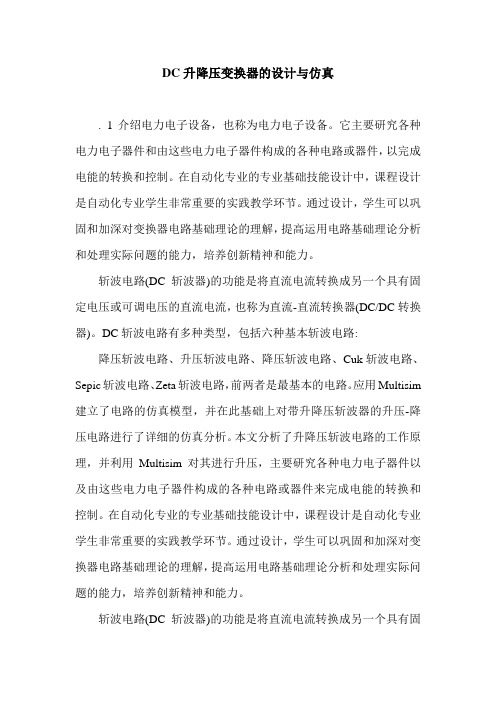
DC升降压变换器的设计与仿真. 1介绍电力电子设备,也称为电力电子设备。
它主要研究各种电力电子器件和由这些电力电子器件构成的各种电路或器件,以完成电能的转换和控制。
在自动化专业的专业基础技能设计中,课程设计是自动化专业学生非常重要的实践教学环节。
通过设计,学生可以巩固和加深对变换器电路基础理论的理解,提高运用电路基础理论分析和处理实际问题的能力,培养创新精神和能力。
斩波电路(DC斩波器)的功能是将直流电流转换成另一个具有固定电压或可调电压的直流电流,也称为直流-直流转换器(DC/DC转换器)。
DC斩波电路有多种类型,包括六种基本斩波电路: 降压斩波电路、升压斩波电路、降压斩波电路、Cuk斩波电路、Sepic斩波电路、Zeta斩波电路,前两者是最基本的电路。
应用Multisim 建立了电路的仿真模型,并在此基础上对带升降压斩波器的升压-降压电路进行了详细的仿真分析。
本文分析了升降压斩波电路的工作原理,并利用Multisim对其进行升压,主要研究各种电力电子器件以及由这些电力电子器件构成的各种电路或器件来完成电能的转换和控制。
在自动化专业的专业基础技能设计中,课程设计是自动化专业学生非常重要的实践教学环节。
通过设计,学生可以巩固和加深对变换器电路基础理论的理解,提高运用电路基础理论分析和处理实际问题的能力,培养创新精神和能力。
斩波电路(DC斩波器)的功能是将直流电流转换成另一个具有固定电压或可调电压的直流电流,也称为直流-直流转换器(DC/DC转换器)。
DC斩波电路有多种类型,包括六种基本斩波电路:降压斩波电路、升压斩波电路、降压斩波电路、Cuk斩波电路、Sepic斩波电路、Zeta斩波电路,前两者是最基本的电路。
应用Multisim 建立了电路的仿真模型,并在此基础上对带升降压斩波器的升压-降压电路进行了详细的仿真分析。
本文分析了升降压斩波电路的工作原理,并利用Multisim对电压进行升压:当可控开关v处于导通状态时,电源e通过v向电感l供电以存储能量,电流为I1,方向如图1所示。
利用LM3478设计50W DC-DC升降压变换器.
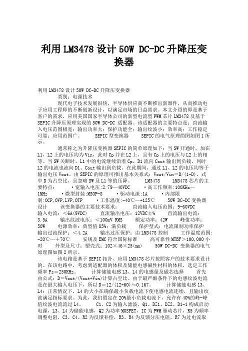
利用LM3478设计50W DC-DC升降压变换器利用LM3478设计50W DC-DC升降压变换器类别:电源技术现代电子技术发展很快,半导体供应商不断推出新器件,从而推动电子应用工程师的不断创新设计,以满足市场的日益需求。
本文介绍的即是基于客户的需求,应用美国国家半导体公司的新型电流型PWM芯片LM3478及基于SEPIC升降压原理实现的50W DC-DC 适配器。
该适配器的主要特点是:直流输入电压范围极宽;输出功率大;保护功能全;输出纹波小;效率高;工作稳定可靠;应用范围广。
SEPIC型变换器SEPIC的电气原理简图如图1所示。
通常称之为升降压变换器SEPIC的简单原理如下:当SW开通时,加在L1,L2上的电压均为Vin,此时Cp并在L2上,且有Cp上的电压与L2上的相等。
当SW关断时,L1中的电流继续沿着Cp、D1流向Cout输出到负载,同时L2的电流也流向D1、Cout输出到负载。
在此期间,通过L1、L2的电压均等于输出电压Vout。
由SEPIC的原理可推出基本关系式:Vout/Vin=D/(1-D)。
式中D为占空比,且忽略SW及L1等的压降。
LM3478 LM3478芯片的主要特点:·宽输入电压:2.79—40VDC ·高工作频率:100KHz—1MHz ·微型封装:MSOP-8 ·驱动电流:1A ·内部限制:OCP,OVP,LVP,OTP ·工作温度:-40℃—+125℃ 50W DC-DC变换器设计该变换器的主要技术要求:直流输入电压范围:9-60VDC输入电流:<6A(9VDC) 直流输出电压:12VDC±% 直流输出电流:3.5A 输出纹波电压:<100mV RMS 额定功率:42W 峰值功率:50W 电源效率:典型值85%;满负载保护型式:电流限制功率保护输出过流保护:<4.2A 输出过压保护:由LM3478控制工作温度范围: -20℃—+70℃ 安规及EMC符合国际标准高可靠性MTBF>100,000小时外型及尺寸:塑壳式;102×46×25(mm) 50W DC-DC 变换器的电气原理图如图2所示。
奥地利微电子推出50V电压的DC—DC升压转换器
奥地利微电子推出50V电压的DC—DC升压转换器
无
【期刊名称】《中国电子商情:基础电子》
【年(卷),期】2008(000)004
【摘要】奥地利微电子公司发布输出电压高达50V的升压转换器AS1340,主要适用于LCD或OLED显示器等需要使用电池供电的解决方案。
【总页数】1页(P84)
【作者】无
【作者单位】无
【正文语种】中文
【中图分类】TN929.53
【相关文献】
1.奥地利微电子新型DC-DC升压转换器可用0.9V输入电压实现42V输出电压[J],
2.奥地利微电子推出具备降压功能的高效200mADC—DC升压转换器 [J], 无
3.奥地利微电子推出具备降压功能的高效200mA DC-DC升压转换器 [J],
4.奥地利微电子推出新款DC-DC升压转换器 [J],
5.奥地利微电子推出新款单节锂离子电池到50V电压的DC-DC升压转换器 [J],因版权原因,仅展示原文概要,查看原文内容请购买。
- 1、下载文档前请自行甄别文档内容的完整性,平台不提供额外的编辑、内容补充、找答案等附加服务。
- 2、"仅部分预览"的文档,不可在线预览部分如存在完整性等问题,可反馈申请退款(可完整预览的文档不适用该条件!)。
- 3、如文档侵犯您的权益,请联系客服反馈,我们会尽快为您处理(人工客服工作时间:9:00-18:30)。
利用LM3478设计50W DC-DC升降压变
换器
利用LM3478设计50W DC-DC升降压变换器
类别:电源技术
现代电子技术发展很快,半导体供应商不断推出新器件,从而推动电
子应用工程师的不断创新设计,以满足市场的日益需求。
本文介绍的即是基于
客户的需求,应用美国国家半导体公司的新型电流型PWM芯片LM3478及基于SEPIC升降压原理实现的50W DC-DC 适配器。
该适配器的主要特点是:直流输
入电压范围极宽;输出功率大;保护功能全;输出纹波小;效率高;工作稳定
可靠;应用范围广。
SEPIC型变换器SEPIC的电气原理简图如图1所示。
通常称之为升降压变换器SEPIC的简单原理如下:当SW开通时,加在
L1,L2上的电压均为Vin,此时Cp并在L2上,且有Cp上的电压与L2上的相等。
当SW关断时,L1中的电流继续沿着Cp、D1流向Cout输出到负载,同时
L2的电流也流向D1、Cout输出到负载。
在此期间,通过L1、L2的电压均等于
输出电压Vout。
由SEPIC的原理可推出基本关系式:Vout/Vin=D/(1-D)。
式
中D为占空比,且忽略SW及L1等的压降。
LM3478 LM3478芯片的主
要特点:·宽输入电压:2.79—40VDC ·高工作频率:100KHz—
1MHz ·微型封装:MSOP-8 ·驱动电流:1A ·内部限
制:OCP,OVP,LVP,OTP ·工作温度:-40℃—+125℃ 50W DC-DC变换器
设计该变换器的主要技术要求:直流输入电压范围:9-60VDC
输入电流:<6A(9VDC) 直流输出电压:12VDC±% 直流输出电流:
3.5A 输出纹波电压:<100mV RMS 额定功率:42W 峰值功率:
50W 电源效率:典型值85%;满负载保护型式:电流限制功率保护
输出过流保护:<4.2A 输出过压保护:由LM3478控制工作温度范围: -20℃—+70℃ 安规及EMC符合国际标准高可靠性MTBF>100,000小时外型及尺寸:塑壳式;102×46×25(mm) 50W DC-DC 变换器的电气原理图如图2所示。
该电路是基于SEPIC拓扑、应用LM3478芯片按照客户的技术要求设计的。
在该电路中,考虑到适配器的体积及储能电感磁性材料的体积,选定工作
频率Fs=250KHz。
计算储能电感L3、L4的电感量及磁芯选择首先
由公式:D=Vout/(Vout+Vin)计算占空比。
由于最严酷条件下的电感纹波电流
是在最大输入电压下,所以D=12/(12+60)≈0.167。
计算储能电感l3、
L4:正常情况下,L4的大小在确保最小负载电流下使电感电流连续,且输出纹
波满足指标要求。
为此,我们假定在20%最小负载电流下,允许有40%的峰-峰
值纹波电流流过L4。
C1、C2为输入滤波,Q1、DZ1、DZ2、D1-1构成启动
电源,L3、L4为储能电感,Q2为功率MOSFET,IC为PWM驱动芯片,R5为频率
调整电阻,C3、C4、R2为反馈补偿,R3、R4为反馈分压电阻,R7为过电流取
样电阻,C8、C9为SEPIC电容,R8、R9、C6、C7为吸收网络,D2为输出整流
二极管,C10、C11、C12为输出滤波电容。
当然要想符合EMC要求,输入端还
应该有共模电感,差模电感,及X、Y等安规电容。
L=V×dt/di;
其中dt=1/Fs×D=1/(250×103)×0.167≈0.668,V为Vin在MOSFET开通时的值。
因此,有如下计算:L4=60×(0.668×10-6/0.4)=100.2μH。
取100μH的标称值。
由该SEPIC原理及设计经验可知,作为俩个分离的储能电感,L3的取值也为:100μH。
由于该电感为储能电感,因此,对磁性材
料的选取要特别注意。
此处选择的材料为:Magnetic公司的Kool Mu,相同性能的材料,其他公司又称铁硅铝。
参数如下:·料号:77381-A7,黑色·尺寸:17.27×9.65×6.35(mm),为环型磁芯·电感因数AL:43(nH/N2),N为圈数由公式:L=AL×N2,可以计算出电感圈数为:
48圈,且用AWG18号线绕制。
L3、L4相同参数。
·Magnetic公司的Kool Mu材料,损耗少,相对成本低,也可以选同规格其他厂商铁硅铝材料。
如果想进一步降低成本也可以选用国产的铁硅铝材料。
上述L3、L4为两个分离电感设计,也可以共用一个储能磁环,只是此时由于耦合电感的存在,计算的电感值为上述值的一半,为50μH。
但成本低些。
PCB注意事项由于为高频DC-DC变换,因此,PCB布线很重要。
区分功率地与信号地的汇流点,驱动IC与MOSFET的关系,输入滤波与输出滤波的位置等。
同时注意分离元件及贴片元件的位置关系。
还要考虑散热器的形状及散热面积。
关键元器件的选择及说明功率MOSFET的选择:N-FET,极低导通电阻,低门极驱动电压:5V—7V,符合PWM-IC要求,TO-220AB封装,100V/85A,结温175℃。
型号为VISHAY:SUP85N10-10。
肖特基整流二极管的选择:型号为
MBR20100CT,封装为TO-220AB,100V/20A,正向压降低。
输入、输出滤
波电解电容可由计算公式或经验选取。
C8、C9可由计算公式或实验选择。
取样电阻的参数可由计算及实验来确定。
样机调试中发现的问题及解决方法
按照上述原理及计算参数进行PCB的焊接及调试。
发现问题如下:·由LM3478芯片的特点及典型的EPIC应用来看,比较适合功率等级20W以下的DC-DC变换器。
而此处设计成50WDC-DC变换器,发现PWM驱动MOSFET有些困难,波形畸变及MOSFET功耗大,解决的方法为:在IC的6脚与MOSFET的栅极之间加入一级驱动放大,即由NPN和PNP对管组成的放大级。
·L3、L4均取100μH的电感量在工作时发现:在输出轻载或空载时,输出纹波过大。
经试验发现由电感L3引起的,根据经验及分析将L3的电感量降为50mH即可解决问题。
·IC的2引脚COMP对地的补偿参数C3、C4、R2:若按典型参数试验,发现样机有噪声且不稳定,经试验将C2去掉,结果没有噪声且工作稳定。
·取样电阻R7:由于IC的特点使取样电阻的阀值很低,而且该DC-DC的功率相对较大,致使取样电阻R7的选取比较困难,为了降低成本选用微
阻抗电阻。
结语通过对该DC-DC变换器的拓扑结构及驱动IC的选择,设计出了满足技术要求的50W适配器,虽然调试过程中遇到了一些问题,经过试验分析得到了解决。
从实际应用来看,用此原理设计出50W的电源已经很有优势了。
下一步还要考虑EMC及安规问题来满足国际市场的要求。
实验表明,该适配器可用于宽输入电压范围的DC-DC变换器及对蓄电池充电的场合。