英文电路实验报告
rlc串联电路实验报告
rlc串联电路实验报告篇一:RLC串联谐振电路。
实验报告二、RLC串联谐振电路目的及要求:(1)设计电路(包括参数的选择)(2)不断改变函数信号发生器的频率,测量三个元件两端的电压,以验证幅频特性(3)不断改变函数信号发生器的频率,利用示波器观察端口电压与电流相位,以验证发生谐振时的频率与电路参数的关系(4)用波特图示仪观察幅频特性(5)得出结论进行分析并写出仿真体会。
二阶动态电路的响应(RLC串联)可用二阶微分方程描述的电路成为二阶电路。
此电路在输入为零值时的响应称为零输入相应,在零值初始条件下的响应称为零状态响应。
欠阻尼情况下的衰减系数? 为:??R .2L.其震荡频率?d为:?d?;RLC串联谐振电路条件是:电压U与电流I同相。
z?R?jX?R?j(?L?11?C);当?L??C时,谐振频率为f?f0?1;在电路参数不变的情况下,可调整信号源的频率使电路产生串联谐振;在信号源频率不变的情况下,改变L或C使电路产生串联谐振是。
电路的频率特性,电路的电流与外加电压角频率的关系称为电流的幅频特性。
串联谐振电路总阻抗Z=R,其值最小,如电源电压不变,回路电流I=U/R,其值最大;改变信号源的频率时,可得出电流与频率的关系曲线;三.设计原理:一个优质电容器可以认为是无损耗的(即不计其漏电阻),而一个实际线圈通常具有不可忽略的电阻。
把频率可变的正弦交流电压加至电容器和线圈相串联的电路上。
若R、L、C和U的大小不变,阻抗角和电流将随着信号电压频率的改变而改变,这种关系称之为频率特性。
当信号频率为f=f0?现象,且电路具有以下特性:(1)电路呈纯电阻性,所以电路阻抗具有最小值。
(2)I=I。
=U/R即电路中的电流最大,因而电路消耗的功率最大。
同时线圈磁场和电容电时,即出现谐振厂之间具有最大的能量互换。
工程上把谐振时线圈的感抗压降与电源电压之比称之为线圈的品质因数Q。
四.RLC串联谐振电路的设计电路图:自选元器件及设定参数,通过仿真软件观察并确定RLC 串联谐振的频率,通过改变信号发生器的频率,当电阻上的电压达到最大值时的频率就是谐振频率。
大学物理实验报告英文版
大学物理实验报告Ferroelectric Control of Spin PolarizationControlling the spin degree of freedom by purely electrical means is currently an important challenge in spintronics (1, 2). Approaches based on spin-transfer torque (3) have proven very successful in controlling the direction of magnetization in a ferromagnetic layer, but they require the injection of high current densities. An ideal solution would rely on the application of an electric field across an insulator, as in existing nanoelectronics. Early experiments have demonstrated the volatile modulation of spin-based properties with a gate voltage applied through a dielectric. Notable examples include the gate control of the spin-orbit interaction in III-V quantum wells (4), the Curie temperature T C(5), or the magnetic anisotropy (6) in magnetic semiconductors with carrier-mediated exchange interactions; for example, (Ga,Mn)As or (In,Mn)As. Electric field–induced modifications of magnetic anisotropy at room temperature have also been reported recently in ultrathin Fe-based layers (7, 8).A nonvolatile extension of this approach involves replacing the gate dielectric by a ferroelectric and taking advantage of the hysteretic response of its order parameter (polarization) with an electric field. When combined with (Ga,Mn)As channels, for instance, a remanent control of T C over a few kelvin was achieved throughpolarization-driven charge depletion/accumulation (9, 10), and the magnetic anisotropy was modified by the coupling of piezoelectricity and magnetostriction (11, 12). Indications of an electrical control of magnetization have also been provided in magnetoelectric heterostructures at room temperature (13–17).Recently, several theoretical studies have predicted that large variations of magnetic properties may occur at interfaces between ferroelectrics and high-T C ferromagnets such as Fe (18–20), Co2MnSi (21), or Fe3O4(22). Changing the direction of the ferroelectric polarization has been predicted to influence not only the interfacial anisotropy and magnetization, but also the spin polarization. Spin polarization [., the normalized difference in the density of states (DOS) of majority and minority spin carriers at the Fermi level (E F)] is typically the key parameter controlling the response of spintronics systems, epitomized by magnetic tunnel junctions in which the tunnel magnetoresistance (TMR) is related to the electrode spin polarization by the Jullière formula (23). These predictions suggest that the nonvolatile character of ferroelectrics at the heart of ferroelectric random access memory technology (24) may be exploited in spintronics devices such as magnetic random access memories or spin field-effect transistors (2). However, the nonvolatile electrical control of spin polarization has not yet been demonstrated.We address this issue experimentally by probing the spin polarization of electrons tunneling from an Fe electrode through ultrathin ferroelectric BaTiO3(BTO) tunnel barriers (Fig. 1A). The BTO polarization can be electrically switched to point toward or away from the Fe electrode. We used a half-metallic (25) bottom electrode as a spin detector in these artificial multiferroic tunnel junctions (26, 27). Magnetotransport experiments provide evidence for a large and reversible dependence of the TMR on ferroelectric polarization direction.Fig. 1(A) Sketch of the nanojunction defined by electrically controlled nanoindentation. A thin resist is spin-coated on the BTO(1 nm)/LSMO(30 nm) bilayer. The nanoindentation is performed with a conductive-tip atomic force microscope, and the resulting nano-hole is filled by sputter-depositing Au/CoO/Co/Fe. (B) (Top) PFM phase image of a BTO(1 nm)/LSMO(30 nm) bilayer after poling the BTO along 1-by-4–μm stripes with either a negative or positive (tip-LSMO) voltage. (Bottom) CTAFM image of an unpoled area of a BTO(1 nm)/LSMO(30 nm) bilayer. Ω, ohms. (C) X-ray absorption spectra collected at room temperature close to the Fe L3,2(top), Ba M5,4(middle), and Ti L3,2(bottom) edges on an AlO x nm)/Al nm)/Fe(2 nm)/BTO(1 nm)/LSMO(30 nm)(D) HRTEM and (E) HAADF images of the Fe/BTO interface in a Ta(5 nm)/Fe(18 nm)/BTO(50 nm)/LSMO(30 nm)The white arrowheads in (D) indicate the lattice fringes of {011} planes in the iron layer. [110] and [001] indicate pseudotetragonal crystallographic axes of the BTO perovskite.The tunnel junctions that we used in this study are based on BTO(1 nm)/LSMO(30 nm) bilayers grown epitaxially onto (001)-oriented NdGaO3(NGO) single-crystal substrates (28). The large (~180°) and stable piezoresponse force microscopy (PFM) phase contrast (28) between negatively and positively poled areas (Fig. 1B, top) indicates that the ultrathin BTO films are ferroelectric at room temperature (29). The persistence of ferroelectricity for such ultrathin films of BTO arises from the large lattice mismatch with the NGO substrate (–%), which is expected to dramatically enhance ferroelectric properties in this highly strained BTO (30). The local topographical and transport properties of the BTO(1 nm)/LSMO(30 nm) bilayers were characterized by conductive-tipatomic force microscopy (CTAFM) (28). The surface is very smooth with terraces separated by one-unit-cell–high steps, visible in both the topography (29) and resistance mappings (Fig. 1B, bottom). No anomalies in the CTAFM data were observed over lateral distances on the micrometer scale.We defined tunnel junctions from these bilayers by a lithographic technique based on CTAFM (28, 31). Top electrical contacts of diameter ~10 to 30 nm can be patterned by this nanofabrication process. The subsequent sputter deposition of a 5-nm-thick Fe layer, capped by a Au(100 nm)/CoO nm)/Co nm) stack to increase coercivity, defined a set of nanojunctions (Fig. 1A). The same Au/CoO/Co/Fe stack was deposited on another BTO(1 nm)/LSMO(30 nm) sample for magnetic measurements. Additionally, a Ta(5 nm)/Fe(18 nm)/BTO(50 nm)/LSMO(30 nm) sample and a AlO x nm)/Al nm)/Fe(2 nm)/BTO(1 nm)/LSMO(30 nm) sample were realized for structural and spectroscopic characterizations.We used both a conventional high-resolution transmission electron microscope (HRTEM) and the NION UltraSTEM 100 scanning transmission electron microscope (STEM) to investigate the Fe/BTO interface properties of the Ta/Fe/BTO/LSMO sample. The epitaxial growth of the BTO/LSMO bilayer on the NGO substrate was confirmed by HRTEM andhigh-resolution STEM images. The low-resolution, high-angle annular dark field (HAADF) image of the entire heterostructure shows the sharpness of the LSMO/BTO interface over the studied area (Fig. 1E, top). Figure 1D reveals a smooth interface between the BTO and the Fe layers. Whereas the BTO film is epitaxially grown on top of LSMO, the Fe layer consists of textured nanocrystallites. From the in-plane (a) and out-of-plane (c) lattice parameters in the tetragonal BTO layer, we infer that c/a= ± , in good agreement with the value of found with the use of x-ray diffraction (29). The interplanar distances for selected crystallites in the Fe layer [., ~ Å(Fig. 1D, white arrowheads)] are consistent with the {011} planes of body-centered cubic (bcc) Fe. We investigated the BTO/Fe interface region more closely in the HAADF mode of the STEM (Fig. 1E, bottom). On the BTO side, the atomically resolved HAADF image allows thedistinction of atomic columns where the perovskite A-site atoms (Ba) appear as brighter spots. Lattice fringes with the characteristic {100} interplanar distances of bcc Fe (~ Å) can be distinguished on the opposite side. Subtle structural, chemical, and/or electronic modifications may be expected to occur at the interfacial boundary between the BTO perovskite-type structure and the Fe layer. These effects may lead to interdiffusion of Fe, Ba, and O atoms over less than 1 nm, or the local modification of the Fe DOS close to E F, consistent with ab initio calculations of the BTO/Fe interface (18–20).To characterize the oxidation state of Fe, we performed x-ray absorption spectroscopy (XAS) measurements on a AlO x nm)/Al nm)/Fe(2 nm)/BTO(1 nm)/LSMO(30 nm) sample (28). The probe depth was at least 7 nm, as indicated by the finite XAS intensity at the La M4,5edge (28), so that the entire Fe thickness contributed substantially to the signal. As shown in Fig. 1C(top), the spectrum at the Fe L2,3edge corresponds to that of metallic Fe (32). The XAS spectrum obtained at the Ba M4,5edge (Fig. 1C, middle) is similar to that reported for Ba2+in (33). Despite the poor signal-to-noise ratio, the Ti L2,3edge spectrum (Fig. C, bottom) shows the typical signature expected for a valence close to 4+ (34). From the XAS, HRTEM, and STEM analyses, we conclude that the Fe/BTO interface is smooth with no detectable oxidation of the Fe layer within a limit of less than 1 nm.After cooling in a magnetic field of 5 kOe aligned along the [110] easy axis of pseudocubic LSMO (which is parallel to the orthorhombic [100] axis of NGO), we characterized the transport properties of the junctions at low temperature K). Figure 2A(middle) shows a typical resistance–versus–magnetic field R(H) cycle recorded at a bias voltage of –2 mV (positive bias corresponds to electrons tunneling from Fe to LSMO). The bottom panel of Fig. 2A shows the magnetic hysteresis loop m(H) of a similar unpatterned sample measured with superconducting quantum interference device (SQUID) magnetometry. When we decreased the magnetic field from a large positive value, theresistance dropped in the –50 to –250 Oe range and then followed a plateau down to –800 Oe, after which it sharply returned to the high-resistance state. We observed a similar response when cycling the field back to large positive values. A comparison with the m(H) loop indicates that the switching fields in R(H) correspond to changes in the relative magnetic configuration of the LSMO and Fe electrodes from parallel (at high field) to antiparallel (at low field). The magnetically softer LSMO layer switched at lower fields (50 to 250 Oe) compared with the Fe layer, for which coupling to the exchange-biased Co/CoO induces larger and asymmetric coercive fields (–800 Oe, 300 Oe). The observed R(H) corresponds to a negative TMR= (R ap–R p)/R ap of –17%[R p and R ap are the resistance in the parallel (p) and antiparallel (ap) magnetic configurations, respectively; see the sketches in Fig. 2A]. Within the simple Jullière model of TMR(23) and considering the large positive spin polarization ofhalf-metallic LSMO (25), this negative TMR corresponds to a negative spin polarization for bcc Fe at the interface with BTO, in agreement with ab initio calculations (18–20).Fig. 2(A) (Top) Device schematic with black arrows to indicate magnetizations. p, parallel; ap, antiparallel. (Middle) R(H) recorded at –2 mV and K showing negative TMR. (Bottom) m(H) recorded at 30 K with a SQUID magnetometer. emu, electromagnetic units.(B) (Top) Device schematic with arrows to indicate ferroelectric polarization.(Bottom) I(V DC) curves recorded at K after poling the ferroelectric down (orange curve) or up (brown curve). The bias dependence of the TER is shown in the inset.As predicted (35–38) and demonstrated (29) previously, the tunnel current across a ferroelectric barrier depends on the direction of the ferroelectric polarization. We also observed this effect in our Fe/BTO/LSMO junctions. As can be seen in Fig. 2B, after poling the BTO at K to orient its polarization toward LSMO or Fe (with a poling voltage of VP–≈ –1 V or VP+≈ 1 V, respectively; see Fig. 2B sketches),current-versus-voltage I(V DC) curves collected at low bias voltages showed a finite difference corresponding to a tunnel electroresistance as large as TER=(I VP+–I VP–)/I VP–≈ 37% (Fig. 2B, inset). This TER can be interpreted within an electrostatic model (36–39), taking into account the asymmetric deformation of the barrier potential profile that is created by the incomplete screening of polarization charges by different Thomas-Fermi screening lengths at Fe/BTO and LSMO/BTO interfaces. Piezoelectric-related TER effects (35, 38) can be neglected as the piezoelectric coefficient estimated from PFM experiments is too small in our clamped films(29). TER measurements performed on a BTO(1 nm)/LSMO(30 nm) bilayer with the use ofa CTAFM boron-doped diamond tip as the top electrode showed values of ~200% (29). Given the strong sensitivity of the TER on barrier parameters and barrier-electrode interfaces, these two values are not expected to match precisely. We anticipate that the TER variation between Fe/BTO/LSMO junctions and CTAFM-based measurements is primarily the result of different electrostatic boundary conditions.Switching the ferroelectric polarization of a tunnel barrier with voltage pulses is also expected to affect the spin-dependent DOS of electrodes at a ferromagnet/ferroelectric interface. Interfacial modifications of the spin-dependent DOS of the half-metallic LSMO by the ferroelectric BTO are not likely, as no states are present for the minority spins up to ~350 meV above E F(40, 41). For 3d ferromagnets such as Fe, large modificationsof the spin-dependent DOS are expected, as charge transfer between spin-polarized empty and filled states is possible. For the Fe/BTO interface, large changes have been predicted through ab initio calculations of 3d electronic states of bcc Fe at the interface with BTO by several groups (18–20).To experimentally probe possible changes in the spin polarization of the Fe/BTO interface, we measured R(H) at a fixed bias voltage of –50 mV after aligning the ferroelectric polarization of BTO toward Fe or LSMO. R(H) cycles were collected for each direction of the ferroelectric polarization for two typical tunnel junctions of the same sample (Fig. 3, B and C, for junction #1; Fig. 3, D and E, for junction #2). In both junctions at the saturating magnetic field, high- and low-resistance states are observed when the ferroelectric polarization points toward LSMO or Fe, respectively, with a variation of ~ 25%. This result confirms the TER observations in Fig. 2B.Fig. 3(A) Sketch of the electrical control of spin polarization at the Fe/BTO interface.(B and C) R(H) curves for junction #1 (V DC= –50 mV, T= K) after poling the ferroelectric barrier down or up, respectively. (D and E) R(H) curves for junction #2 (V DC= –50 mV, T= K) after poling the ferroelectric barrier down or up, respectively. More interestingly, here, the TMR is dramatically modified by the reversal of BTO polarization. For junction #1, the TMR amplitude changes from –17 to –3% when the ferroelectric polarization is aligned toward Fe or LSMO, respectively (Fig. 3, B and C). Similarly for junction #2, the TMR changes from –45 to –19%. Similar resultswere obtained on Fe/BTO nm)/LSMO junctions (28). Within the Jullière model (23), these changes in TMR correspond to a large (or small) spin polarization at the Fe/BTO interface when the ferroelectric polarization of BTO points toward (or away from) the Fe electrode. These experimental data support our interpretation regarding the electrical manipulation of the spin polarization of the Fe/BTO interface by switching the ferroelectric polarization of the tunnel barrier.To quantify the sensitivity of the TMR with the ferroelectric polarization, we define a term, the tunnel electromagnetoresistance, as TEMR= (TMR VP+–TMR VP–)/TMR VP–. Large values for the TEMR are found for junctions #1 (450%) and #2 (140%), respectively. This electrical control of the TMR with the ferroelectric polarization is repeatable, as shown in Fig. 4for junction #1 where TMR curves are recorded after poling the ferroelectric up, down, up, and down, sequentially (28).Fig. 4TMR(H) curves recorded for junction #1 (V DC= –50 mV, T= K) after poling the ferroelectric up (VP+), down (VP–), up (VP+), and down (VP–).For tunnel junctions with a ferroelectric barrier and dissimilar ferromagnetic electrodes, we have reported the influence of the electrically controlled ferroelectric barrier polarization on the tunnel-current spin polarization. This electrical influence over magnetic degrees of freedom represents a new and interfacial magnetoelectric effect that is large because spin-dependent tunneling is very sensitive to interfacial details. Ferroelectrics can provide a local, reversible, nonvolatile, and potentially low-power means of electrically addressing spintronics devices.Supporting Online Materialand MethodsFigs. S1 to S5ReferencesReceived for publication 30 October 2009.Accepted for publication 4 January 2010.References and Notes1. C. Chappert, A. Fert, F. N. Van Dau, The emergence of spinelectronics in data storage. Nat. Mater. 6,813 (2007).2.I. Žutić, J. Fabian, S. Das Sarma, Spintronics: Fundamentalsand applications. Rev. Mod. Phys. 76,323 (2004).3.J. C. Slonczewski, Current-driven excitation of magneticmultilayers. J. Magn. Magn. Mater. 159, L1(1996).4.J. Nitta, T. Akazaki, H. Takayanagi, T. Enoki, Gate control of spin-orbit interaction in an inverted heterostructure. Phys.Rev. Lett. 78, 1335 (1997).5.H. Ohno et al., Electric-field control offerromagnetism. Nature 408, 944 (2000).6. D. Chiba et al., Magnetization vector manipulation by electricfields. Nature 455, 515 (2008).7.M. Weisheit et al., Electric field–induced modification of magnetismin thin-film ferromagnets. Science315, 349 (2007).8.T. Maruyama et al., Large voltage-induced magnetic anisotropy changein a few atomic layers of . Nanotechnol. 4, 158 2009).9.S. W. E. Riester et al., Toward a low-voltage multiferroic transistor:Magnetic (Ga,Mn)As under ferroelectric control. Appl. Phys.Lett. 94, 063504 (2009).10.I. Stolichnov et al., Non-volatile ferroelectric control offerromagnetism in (Ga,Mn)As. Nat. Mater. 7, 464(2008).11. C. Bihler et al., Ga1−x Mn x As/piezoelectric actuator hybrids: A modelsystem for magnetoelastic magnetization manipulation. Phys. Rev.B 78, 045203 (2008).12.M. Overby, A. Chernyshov, L. P. Rokhinson, X. Liu, J.K. Furdyna, GaMnAs-based hybrid multiferroic memory device. Appl. Phys.Lett. 92, 192501 (2008).13. C. Thiele, K. Dörr, O. Bilani, J. Rödel, L. Schultz, Influence of strain on the magnetization and magnetoelectric effectin 75, 054408 (2007).14.W. Eerenstein, M. Wiora, J. L. Prieto, J. F. Scott, N.D. Mathur, Giant sharp and persistent converse magnetoelectric effects inmultiferroic epitaxial heterostructures. Nat. Mater. 6, 348 (2007).15.T. Kanki, H. Tanaka, T. Kawai, Electric control of roomtemperature ferromagnetism in a Pb field-effect transistor. Appl. Phys.Lett. 89, 242506 (2006).16.. Chu et al., Electric-field control of local ferromagnetism using amagnetoelectric multiferroic. Nat. Mater. 7, 478 2008).17.S. Sahoo et al., Ferroelectric control of magnetism in BaTiO3∕Feheterostructures via interface strain coupling. Phys. Rev.B 76, 092108 (2007).18.. Duan, S. S. Jaswal, E. Y. Tsymbal, Predicted magnetoelectriceffect in Fe/BaTiO3multilayers: Ferroelectric control of magnetism. Phys. Rev.Lett. 97, 047201 (2006).19.M. Fechner et al., Magnetic phase transition in two-phasemultiferroics predicted from first . Rev. B 78, 212406 (2008).20.J. Lee, N. Sai, T. Cai, Q. Niu, A. A. Demkov, preprint available at abs/.21.K. Yamauchi, B. Sanyal, S. Picozzi, Interface effects at ahalf-metal/ferroelectric junction. Appl. Phys. Lett. 91, 062506 (2007). 22.M. K. Niranjan, J. P. Velev, . Duan, S. S. Jaswal, E.Y. Tsymbal, Magnetoelectric effect at the Fe3O4/BaTiO3(001) interface: A first-principles study. Phys. Rev. B 78, 104405 (2008).23.M. Jullière,Tunneling between ferromagnetic films. Phys. Lett.A 54, 225 (1975).24.J. F. Scott, Applications of modern ferroelectrics. Science 315, 954 (2007).25.M. Bowen et al., Nearly total spin polarization in La2/3Sr1/3MnO3fromtunneling experiments. Appl. Phys. Lett. 82, 233 (2003).26.J. P. Velev et al., Magnetic tunnel junctions with ferroelectricbarriers: Prediction of four resistance states from first principles. Nano Lett. 9, 427 (2009).27. F. Yang et al., Eight logic states of tunnelingmagnetoelectroresistance in multiferroic tunnel . Appl.Phys. 102, 044504 (2007).28.Materials and methods are available as supporting materialon Science Online.29.V. Garcia et al., Giant tunnel electroresistance for non-destructivereadout of ferroelectric states. Nature460, 81 (2009).30.K. J. Choi et al., Enhancement of ferroelectricity in strainedBaTiO3thin films. Science 306, 1005(2004).31.K. Bouzehouane et al., Nanolithography based on real-timeelectrically controlled indentation with an atomic force microscope fornanocontact elaboration. Nano Lett. 3, 1599 (2003).32.T. J. Regan et al., Chemical effects at metal/oxide interfaces studiedby x-ray-absorption . Rev. B 64, 214422 (2001).33.N. Hollmann et al., Electronic and magnetic properties of the kagomesystems YBaCo4O7and YBaCo3M O7(M=Al, Fe). Phys. Rev. B 80, 085111 (2009).34.M. Abbate et al., Soft-x-ray-absorption studies of the location ofextra charges induced by substitution in controlled-valence materials. Phys. Rev.B 44, 5419 (1991).35. E. Y. Tsymbal, H. Kohlstedt, Tunneling across aferroelectric. Science 313, 181 (2006).36.M. Ye. Zhuravlev, R. F. Sabirianov, S. S. Jaswal, E.Y. Tsymbal, Giant electroresistance in ferroelectric tunnel junctions. Phys.Rev. Lett. 94, 246802 (2005).37.M. Ye. Zhuravlev, R. F. Sabirianov, S. S. Jaswal, E.Y. Tsymbal, Erratum: Giant electroresistance in ferroelectric tunneljunctions. Phys. Rev. Lett. 102, 169901 2009).38.H. Kohlstedt, N. A. Pertsev, J. RodriguezContreras, R. Waser, Theoretical current-voltage characteristics offerroelectric tunnel junctions. Phys. Rev. B 72, 125341 (2005).39.M. Gajek et al., Tunnel junctions with multiferroic barriers. Nat.Mater. 6, 296 (2007).40.M. Bowen et al., Spin-polarized tunneling spectroscopy in tunneljunctions with half-metallic . Rev. Lett. 95, 137203 (2005).41.J. D. Burton, E. Y. Tsymbal, Prediction of electrically inducedmagnetic reconstruction at the manganite/ferroelectric interface. Phys. Rev.B 80, 174406 (2009).42.We thank R. Guillemet, C. Israel, M. E. Vickers, R. Mattana, . George,and P. Seneor for technical assistance, and C. Colliex for fruitful discussions on the microscopy measurements. This study was partially supported by the .Partenariat Hubert Curien Alliance program, the French Réseau Thématique de Recherche Avancée Triangle de la Physique, the European Union (EU) Specific Targeted Research Project (STRep) Manipulating the Coupling in Multiferroic Films, EU STReP Controlling Mesoscopic Phase Separation, . Engineering and Physical Sciences Research Council grant EP/E026206/I, French C-Nano Île de France, French Agence Nationale de la Recherche (ANR) Oxitronics, French ANR Alicante, the European Enabling Science and Technology through European Elelctron Microscopy program, and the French Microscopie Electronique et Sonde Atomique network. .acknowledges support from Comissionat per a Universitats i Recerca (Generalitat de Catalunya).。
英语作文物理电学实验报告

英语作文物理电学实验报告Physics Experiment Report on Electric Circuits。
Introduction。
Electric circuits are important in our daily lives as they form the basis of all electrical devices. In this experiment, we investigated the behavior of electric circuits, including Ohm's law, Kirchhoff's laws, and the behavior of resistors in series and parallel.Materials。
Power supply。
Ammeter。
Voltmeter。
Resistors (varying values)。
Wires。
Breadboard。
Procedure。
1. Set up the circuit as shown in the diagram below, using a breadboard to connect the components.2. Measure the voltage across the resistor using the voltmeter and record the value.3. Measure the current flowing through the resistor using the ammeter and record the value.4. Repeat steps 2-3 for different values of resistors.5. Connect resistors in series and parallel and measure the voltage and current across each resistor.Results。
简易电路制作方法作文

简易电路制作方法作文英文回答:To make a simple circuit, you will need a few basic components: a power source, such as a battery, wires to connect the components, and a load, such as a light bulb or a buzzer.First, gather all the necessary materials. For this example, let's say we want to make a circuit that lights up an LED. We will need a battery, an LED, a resistor, and some wires.Next, connect the positive terminal of the battery to one end of the resistor using a wire. Then, connect the other end of the resistor to the positive terminal of the LED using another wire.After that, connect the negative terminal of the LED to the negative terminal of the battery using a wire.Finally, check your connections and make sureeverything is secure. Once you are satisfied, turn on the power source and the LED should light up.中文回答:制作一个简易电路,你需要几个基本组件,一个电源,比如电池,用于连接组件的导线,以及一个负载,比如一个灯泡或者一个蜂鸣器。
关于逻辑电路英文作文

关于逻辑电路英文作文英文:Logic circuits are essential components in modern electronics. They are used to process and manipulatedigital signals, which are represented by binary numbers. These circuits are made up of logic gates, which are the building blocks of digital electronics. There are several types of logic gates, including AND, OR, NOT, NAND, and NOR gates.AND gates produce an output signal only when both input signals are high. OR gates produce an output signal when either input signal is high. NOT gates invert the input signal, producing the opposite output signal. NAND gates produce an output signal when either input signal is low, while NOR gates produce an output signal only when both input signals are low.Logic circuits can be combined to create more complexcircuits, such as adders and multipliers. For example, an adder circuit takes two binary numbers as input and produces their sum as output. A multiplier circuit takes two binary numbers as input and produces their product as output.In addition to their use in digital electronics, logic circuits are also used in computer science and programming. Boolean algebra, which is the mathematical foundation of digital electronics, is used to represent and manipulate logical expressions.Overall, logic circuits are an essential component in modern electronics and computer science. They allow us to process and manipulate digital signals, which are the foundation of modern technology.中文:逻辑电路是现代电子学中不可或缺的组成部分。
英文版——模拟电路实验、国际交流班
实验一单级交流放大电路Experiment Single-stage ac amplifying circuit一、实验目的I. Objectives1.熟悉电子元器件和模拟电路实验箱,2.掌握放大电路静态工作点的调试方法及其对放大电路性能的影响。
1. Electronic components and analog circuit experiment box should be familiar-ed .2. The debugging method of amplifier circuit static working point and its effect on the performance of amplifier circuit should be mastered.二、实验仪器II.Experimental apparatus1.示波器2.信号发生器3.数字万用表1. The Oscilloscope2. Signal generator3. Digital multimeter三、预习要求III. Preview requirements1.三极管及单管放大电路工作原理。
2.放大电路静态测量方法。
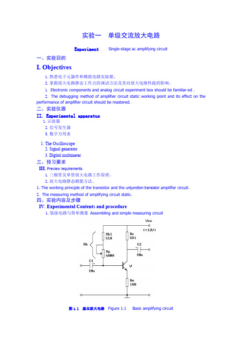
1. The working principle of the transistor and the unijunction transistor amplifier circuit.2. The measuring method of amplifying circuit static.四、实验内容及步骤IV. Experimental Contents and procedure1.装接电路与简单测量Assembling and simple measuring circuit图1.l 基本放大电路Figure 1.1 Basic amplifying circuit(1)用万用表判断实验箱上三极管V的极性和好坏。
英语作文实验报告
英语作文实验报告English Essay on Experiment Report。
The first thing I noticed when I started the experiment was how exciting it felt to be part of something scientific. It's not just about following steps; it's about exploring and learning. You never quite know what's going to happen, and that makes it all the more thrilling.During the process, I had to be really careful with the measurements. You know, a little too much or too little of something can completely change the outcome. But it was fun to see how everything interacted and affected each other.It's like a puzzle that you have to solve.One of the coolest moments was when I saw the first signs of a reaction. It was like, "Whoa! This is actually happening!" You can read about it in books, but seeing it with your own eyes is a completely different experience.After that, it was just a matter of waiting and observing. Sometimes, it felt like nothing was happening, but then suddenly, there'd be a change. It taught me patience, which is not always my strong suit.When it was all done, I felt a sense of accomplishment. Not just because the experiment worked, but because I didit myself. I learned so much about the process and the science behind it. It made me want to do more experiments and explore more.Looking back, I realize that experiments are not just about getting results. They're about the journey, about the process of discovery。
基本电路实验英文示范报告

No. Date: Student number: Name:
1
Title: BASIC ELECTRICITY
【Aim 】
【
Theory 】
【Table】
Graph
要求:以电流为横坐标,电压为纵坐标作图,可以用坐标纸(包括打印的坐标纸)手绘(注意必须按照要求建立坐标系、描点、连线),后拍照(图名边上写上名字拍照)插入此处,也可以excel作图和截屏(例子如下)插入此处,注意数据应该与测量的数据一致。
【Results】
【Conclusions】
Score: T A: Date :
注意事项:
实验过程要按照要求“保存状态”。
要求三张截屏以验证完成实验情况,截屏中数据与实验报告中数据一致。
截屏一:要求有学生名字,电阻部分全部测完,万用表保留在测量最后一项的状态,图片清晰度要够高,放大后可以看清楚。
截屏2:要求有学生名字,二极管与电容测完,保留在电容测量状态
截屏3:要求学生名字,电流表放大图,对应最后一个测量数据。
附录一:坐标纸
如果没有地方买坐标纸可以找地方打印后在上面作图,然后再拍照,如果文具店有坐标纸优先买坐标纸作图。
附录二:excel添加趋势线(不要求截图上传,仅供大家参考),注意线性/截距/显示公式。
怎么用excel作“散点图”可以上网查询。
英文的物理实验报告

英文的物理实验报告英文的物理实验报告IntroductionIn the field of science, conducting experiments and documenting the results is an essential part of the research process. This holds true for physics as well, where experimental reports play a crucial role in presenting and analyzing the findings. In this article, we will explore the structure and content of an English physics experiment report, highlighting its importance and providing tips for effective writing.Experimental SetupThe first section of a physics experiment report typically outlines the experimental setup. Here, the writer describes the apparatus used, including any instruments, equipment, and materials. It is essential to provide sufficient details so that readers can understand and replicate the experiment if needed. Clear and concise language should be used to ensure accuracy and avoid any ambiguity.MethodologyThe methodology section explains the step-by-step procedure followed during the experiment. It should be written in a logical and sequential manner, allowing readers to understand the experimental process easily. It is advisable to use active voice and past tense when describing the actions performed during the experiment. Additionally, any calculations or formulas used should be clearlystated, ensuring transparency and reproducibility.Data Collection and AnalysisAfter conducting the experiment, the next step is to collect and analyze the data obtained. In this section, the writer presents the raw data gathered during the experiment. This can be done using tables, graphs, or charts, depending on the nature of the data. It is important to label and title all figures appropriately, providing units of measurement and clear legends.Once the data is presented, the analysis begins. The writer interprets the data, looking for patterns, trends, and relationships. Statistical methods, such as calculating averages or standard deviations, may be employed to support the analysis. It is crucial to provide a clear and logical explanation of the findings, relating them back to the objectives of the experiment.DiscussionThe discussion section is where the writer provides a deeper analysis of the results obtained. This is an opportunity to compare the findings with existing theories or prior research. Any discrepancies or unexpected outcomes should be addressed and explained. The writer may also suggest possible sources of error or limitations of the experiment, demonstrating a critical understanding of the experimental process.ConclusionThe conclusion summarizes the key findings of the experiment and their implications. It should be concise and to the point, highlighting the significanceof the results. The writer may also mention any recommendations for further research or improvements to the experimental setup. It is important to avoid introducing any new information in the conclusion, as it should serve as a summary of the report.ReferencesIn scientific writing, it is crucial to acknowledge the sources of information used. The references section provides a list of all the references cited in the report. The writer should follow a specific citation style, such as APA or MLA, and provide complete and accurate information for each reference. This ensures credibility and allows readers to explore the sources further if desired.ConclusionWriting an English physics experiment report requires careful attention to detail and a clear understanding of the scientific method. By following the structure outlined above and focusing on clarity and accuracy, researchers can effectively communicate their experimental findings. Experiment reports serve as a valuable tool for the scientific community, facilitating knowledge sharing and promoting further research and discovery.。
rl电路实验报告
rl电路实验报告RC一阶电路的响应测试实验报告实验七RC一阶电路的响应测试一、实验目的1. 测定RC一阶电路的零输入响应、零状态响应及完全响应。
2. 学习电路时间常数的测量方法。
3. 掌握有关微分电路和积分电路的概念。
4. 进一步学会用示波器观测波形。
二、原理说明1. 动态网络的过渡过程是十分短暂的单次变化过程。
要用普通示波器观察过渡过程和测量有关的参数,就必须使这种单次变化的过程重复出现。
为此,我们利用信号发生器输出的方波来模拟阶跃激励信号,即利用方波输出的上升沿作为零状态响应的正阶跃激励信号;利用方波的下降沿作为零输入响应的负阶跃激励信号。
只要选择方波的重复周期远大于电路的时间常数τ,那么电路在这样的方波序列脉冲信号的激励下,它的响应就和直流电接通与断开的过渡过程是基本相同的。
2.图7-1(b)所示的RC 一阶电路的零输入响应和零状态响应分别按指数规律衰减和增长,其变化的快慢决定于电路的时间常数τ。
3. 时间常数τ的测定方法:用示波器测量零输入响应的波形如图7-1(a)所示。
根据一阶微分方程的求解得知uc=Ume-t/RC=Ume-t/τ。
当t=τ时,Uc(τ)=0.368Um。
此时所对应的时间就等于τ。
亦可用零状态响应波形增加到0.632Um所对应的时间测得,如图13-1(c)所示。
Umc Um0.632 ca) 零输入响应(b) RC一阶电路(c) 零状态响应图7-14. 微分电路和积分电路是RC一阶电路中较典型的电路,它对电路元件参数和输入信号的周期有着特定的要求。
一个简单的RC 串联电路,在方波序列脉冲的重复激励下,当utt满足τ=RCT时(T为方波脉冲的重复周期),且由R两端的电压作为响应输出,则该2电路就是一个微分电路。
因为此时电路的输出信号电压与输入信号电压的微分成正比。
如图7-2(a)所示。
利用微分电路可以将方波转变成尖脉冲。
C (a)微分电路(b) 积分电路图7-2若将图7-2(a)中的R与C位置调换一下,如图13-2(b)所示,由C 两端的电压作为响应输出,且当电路的参数满足τ=RCT,则该RC电路称为积分电路。
英语作文实验报告

英语作文实验报告Yesterday, we conducted an experiment in the lab totest the effects of different temperatures on the growth of plants. The goal was to observe how plants react to extreme temperatures and whether they can adapt to survive in harsh conditions.The experiment started by planting seeds in separate pots and placing them in different temperature-controlled environments. Some pots were kept in a room with normal room temperature, while others were placed in a freezer or a heated room. We wanted to see if the plants would grow differently depending on the temperature they were exposed to.After a week of observation, we found that the plants in the normal room temperature environment grew the best. They had healthy green leaves and strong stems. On the other hand, the plants in the freezer environment wilted and died, unable to withstand the extreme cold. The plantsin the heated room also struggled to grow, with yellow leaves and stunted growth.Overall, the experiment showed us the importance of maintaining a stable temperature for plant growth. Extreme temperatures can have a negative impact on plants, affecting their ability to photosynthesize and grow. It is crucial to provide plants with the right conditions to ensure their survival and well-being.In conclusion, this experiment provided valuable insights into the effects of temperature on plant growth. It highlighted the need for careful monitoring and control of environmental conditions to support healthy plant development. By understanding how plants respond to different temperatures, we can better protect and nurture them in various settings.。
英文实验报告

英文实验报告英文实验报告Introduction:In today's globalized world, English has become a crucial skill for communication and career advancement. As a result, English language learners often participate in various experiments and studies to enhance their language proficiency. This article aims to explore the importance of English experiments and the benefits they offer.1. The Purpose of English Experiments:English experiments serve multiple purposes, including language acquisition, pronunciation improvement, vocabulary expansion, and cultural understanding. These experiments provide learners with a hands-on approach to language learning, allowing them to apply theoretical knowledge in real-life situations. 2. Language Acquisition:One of the primary goals of English experiments is to facilitate language acquisition. Through interactive activities, learners have the opportunity to practice listening, speaking, reading, and writing skills. Engaging in conversations with native speakers or participating in group discussions helps learners develop fluency and gain confidence in their language abilities.3. Pronunciation Improvement:English experiments often focus on improving pronunciation, as it plays a vital role in effective communication. Learners can engage in activities such astongue twisters, mimicking native speakers, or recording their own voices to identify areas of improvement. By practicing correct pronunciation, learners can enhance their spoken English and minimize misunderstandings.4. Vocabulary Expansion:English experiments provide learners with exposure to a wide range of vocabulary. Whether it's through reading materials, listening exercises, or interactive games, learners can encounter new words and phrases. This exposure helps them expand their vocabulary, improve word choice, and develop a more nuanced understanding of the English language.5. Cultural Understanding:Language and culture are deeply intertwined. English experiments often incorporate cultural aspects to provide learners with a holistic learning experience. By exploring cultural traditions, customs, and idiomatic expressions, learners gain a deeper understanding of the English-speaking world. This cultural knowledge enhances their ability to communicate effectively and adapt to different social contexts.6. Benefits of English Experiments:Participating in English experiments offers numerous benefits to learners. Firstly, it provides a supportive and immersive environment for language practice, allowing learners to make mistakes and learn from them. Secondly, experiments encourage active engagement, fostering a deeper understanding of language structures and usage. Lastly, English experiments promote self-reflection andself-assessment, enabling learners to monitor their progress and set realistic goals for improvement.Conclusion:English experiments play a crucial role in language acquisition and overall language proficiency. By engaging in various activities, learners can enhance their speaking, listening, reading, and writing skills. Moreover, these experiments provide learners with exposure to different cultural aspects, enriching their language learning experience. The benefits of English experiments extend beyond language acquisition, as they also promote self-reflection and foster a lifelong love for learning. Therefore, it is essential for English language learners to actively participate in experiments to maximize their language learning potential.。
英文实验报告总结模板

Title:[Experiment Name]Date of Experiment:[Date]Objective:To [state the main objective of the experiment].Materials:- [List all materials used in the experiment, including equipment, chemicals, and any other necessary items.]Procedure:1. [Step 1 of the procedure]2. [Step 2 of the procedure]3. [Step 3 of the procedure]...[Continue listing all steps in the procedure.]Data Collection:- [Description of how data was collected, including measurements, observations, and any other relevant information.]Data Analysis:- [Summary of the data analysis techniques used, such as calculations, graphs, or statistical tests.]Results:- [Present the results of the experiment in a clear and concise manner. Include tables, graphs, or charts as necessary.]Discussion:- [Interpret the results and discuss their significance. Compare the results to expected outcomes or previous studies. Address any anomalies or unexpected results.]- Anomaly 1:- [Description of the anomaly]- [Possible reasons for the anomaly]- [Impact on the experiment and conclusions]- Anomaly 2:- [Description of the anomaly]- [Possible reasons for the anomaly]- [Impact on the experiment and conclusions]- [Continue with any additional anomalies or interesting observations.]Conclusion:- [Summarize the main findings of the experiment and their implications. Restate the objective and whether it was achieved.]Recommendations:- [Suggest any improvements or modifications to the experiment procedure or equipment. Propose further studies or applications of the findings.]References:- [List all sources cited in the report, including textbooks, journal articles, and online resources.]Appendix:- [Include any additional information, such as detailed data tables, raw data, or additional figures that support the findings of the experiment.]---Example:Title:Investigation of the Effect of Temperature on the Rate of PhotosynthesisDate of Experiment:March 15, 2023Objective:To determine the effect of varying temperatures on the rate of photosynthesis in spinach leaves.Materials:- Spinach leaves- Light source- Beakers- Thermometer- Stopwatch- Sodium bicarbonate solution- pH test strips- Distilled waterProcedure:1. Prepared spinach leaves by removing stems and rinsing them under tap water.2. Placed equal amounts of spinach leaves in each beaker.3. Prepared a sodium bicarbonate solution with varying concentrations.4. Divided the beakers into groups, each with a different temperature(e.g., 10°C, 20°C, 30°C, 40°C).5. Submerged the leaves in the respective solutions and measured the pH using pH test strips.6. Taped a light source above each beaker and recorded the time it took for the pH to increase by 1 unit.7. Repeated the experiment three times to ensure accuracy.Data Collection:- pH increase over time for each temperature group.Data Analysis:- Calculated the average time for pH increase for each temperature group.Results:- [Insert table or graph showing the average time for pH increase at each temperature.]Discussion:- The data shows that the rate of photosynthesis increases with temperature up to a certain point, after which it begins to decrease. This is consistent with the hypothesis that temperature affects the rate of enzyme activity in photosynthesis.- At lower temperatures (10°C and 20°C), the rate of photosynthesis was significantly slower, indicating the importance of optimal temperature for enzyme activity.- At higher temperatures (30°C and 40°C), the rate of photosynthesis increased but then decreased, suggesting a possible denaturation of enzymes at very high temperatures.Conclusion:The experiment confirmed that temperature significantly affects the rate of photosynthesis in spinach leaves. The optimal temperature for photosynth esis in this study was found to be around 30°C.Recommendations:- Further studies should investigate the specific temperature rangesthat are optimal for photosynthesis in different plant species.- The experiment could be modified to include more temperature groups and a wider range of temperatures to observe the exact point of enzyme denaturation.References:- [List of references used in the report.]Appendix:- [Include any additional information, such as detailed data tables, raw data, or additional figures.]。
Pspice电路仿真实验报告

实验报告院(系):学号:专业:实验人:实验题目:运用Pspice软件进行电路仿真实验。
一、实验目的1、通过实验了解并掌握Pspice软件的运用方法,以及电路仿真的基本方法。
2、学会用电路仿真的方法分析各种电路。
3、通过电路仿真的方法验证所学的各种电路基础定律,并了解各种电路的特性。
二、软件简介Pspice是主要用于集成电路的分析程序,Pspice起初用在大规模电子计算机上进行仿真分析,后来推出了能在 PC上运行的Pspice软件。
Pspice5.0以上版本是基于windows 操作环境。
Pspice软件的主要用途是用于于仿真设计:在实际制作电路之前,先进行计算机模拟,可根据模拟运行结果修改和优化电路设计,测试各种性能,不必涉及实际元器件及测试设备。
三、具体实验内容A、电阻电路(实验一exe 3.38、实验二exe 3.57)1、原理说明:对于简单的电阻电路,用Pspice软件进行电路的仿真分析时,现在要在capture环境(即Schematics程序)下画出电路图。
然后调用分析模块、选择分析类型,就可以“自动”进行电路分析了。
Pspice软件是采用节点电压法求电压的,因此,在绘制电路图时,一定要有零点(即接地点)。
同时,要可以用电路基础理论中的方法列电路方程,求解电路中各个电压和电流。
与仿真结果进行对比分析2、步骤:(1)打开Schematics程序,进入画图界面。
(2)原理图界面点击Get New Part图标,添加常用库,点击Add Library ,将常用库添加进来。
本例需添加Analog( 包含电阻、电容等无源器件),Soure(包含电压源、电流源等电源器件)。
在相应的库中选取电阻R,电压源IDC, F1(实验一),以及地线GND,点取Place 放到界面上。
(3)调节好各元件的位置以及方向,并设好大小,最后连线,保存。
(4)按键盘“F11”(或界面smulate图标)开始仿真。
如原理图无错误,则显示Pspice A/D 窗口。
英文科技小实验-简单电路

Simple Electric CircuitThe Simple Electric Circuit will helpyou to learn the basic concepts ofelectricity and electrical circuits. Youwill experience and build a light circuitpowered by a battery and controlledby a switch. You will also learn aboutelectrical conductors and insulators.You will receive all the componentsand you must build the circuit bycutting the wire and connecting theparts according to the diagram in thispage.Connection of wires to the battery holder, switch and the lamp base are done using the screws or clips. You can use household tools such as a pair of scissors to cut the wire and remove the insulation from the contact points. You will also need a D size battery to power your circuit.Electricity and Conductivity Science Kit includes several experiments in Electrical Circuits, conductivity and properties of electricity. Some of the project ideas you may have using this kit are:1- Construct a Simple Electric Circuit (Grades 2 to 5)2- Can electricity create heat? (Grades 4 to 6, You will need a thermometer to show that the light bulb is getting hot.)3- Construct a Continuity tester and test conductivity of objects around you.The Simple Electric Circuit Kit includes:∙Wooden base to mount the circuit∙ 2 Light Bulbs∙ 1 lamp holder∙ 1 Battery holders∙ 1 Simple Switch (Known as knife switch)∙Screws used to mount the switch and the lamp holder∙Insulated solid copper wire (Gage 22)Opportunities for Science ProjectsYou may use your kit in relation to many different science projects. Construction of a simple electric circuit by itself may be used as a science project for many different grades. You may also use some color paper to make a nice lamp shade for it and use it as your night light. Some other students may need to use their completed circuitto do further research for their science project. Two common project ideas that use this kit are:1.Can electricity create heat? To do this project you will also need athermometer to show that the light bulb is getting hot.2.Identify conductors and insulators around you. It is important to know whatmaterials are conductive and what materials are not. The test is simple.Open the switch and place the object between the poles of the switch. If the light comes on, then the object is conductive. You may try this with metals (coins, paper clips, nails, etc.) and non-metals (glass, plastic, stone, wood, etc.)。
RLC电路特性的研究实验报告
4700Ω 2
L C
计算得:临界阻尼时电阻 R 理论值 相对误差: 34.8% 4 RLC 谐振电路 数据: R 1900Ω L
7211Ω
13mH C
1nF
f/KHz UR /V U/V cos φ φ f/KHz UR /V U/V cos φ 1.007 0.0643 5.28 0.012 ‐1.559 45.21 4.53 4.85 0.934 7.05 0.456 5.18 0.088 ‐1.483 55.85 3.86 4.94 0.781 13.16 0.893 5.16 0.173 ‐1.397 60.53 3.46 5.01 0.691 17.21 1.21 5.14 0.235 ‐1.333 67.16 2.89 5.06 0.571 21.98 1.63 5.04 0.323 ‐1.241 76.92 2.26 5.08 0.445 25.71 2.02 4.98 0.406 ‐1.153 87.72 1.80 5.07 0.355 28.63 2.36 4.91 0.481 ‐1.069 101.5 1.44 5.08 0.283 31.36 2.70 4.87 0.554 ‐0.983 123.8 1.04 5.08 0.205 34.07 3.08 4.82 0.639 ‐0.878 162.2 0.670 5.10 0.131 36.44 3.46 4.82 0.718 ‐0.770 242.5 0.303 5.10 0.059 39.43 3.91 4.77 0.820 ‐0.610 345.5 0.119 4.94 0.024
6 7 8 9
为保证波形稳定显示,在正确选择了触发源的前提下,还应注意调节触发电平旋钮 (LEVEL)。 示波器显示波形时,水平方向一般应调到两到三个周期,垂直方向则应调到波形的高度 占到满屏的三分之二或一半以上。 不要使示波器长时间停留于 X‐Y 方式,这样光点停留在一点不动,会使电子束长时间轰 击屏幕一点,会在荧光屏上形成暗斑,损坏荧光屏。 在观察过程中,应避免经常启闭电源。示波器暂时不用时不必断开电源,只需调节辉度 旋钮使亮点消失,到下次使用时再调节亮。因为每次电源接通时,示波管的灯丝尚处于 冷态,电阻很小,通过的电流很大,会缩短示波管寿命。
电路实验报告(8篇)

电路实验报告(8篇)电路实验报告(8篇)电路实验报告1一、实验题目利用类实现阶梯型电阻电路计算二、实验目的利用类改造试验三种构造的计算程序,实现类的封装。
通过这种改造理解类实现数据和功能封装的作用,掌握类的设计与编程。
三、实验原理程序要求用户输入的电势差和电阻总数,并且验证数据的有效性:电势差必须大于0,电阻总数必须大于0小于等于100的偶数。
再要求用户输入每个电阻的电阻值,并且验证电阻值的有效性:必须大于零。
此功能是由类CLadderNetwork的InputParameter ()函数实现的。
且该函数对输入的数据进行临界判断,若所输入数据不满足要求,要重新输入,直到满足要求为止。
本实验构造了两个类,一个CResistance类,封装了电阻的属性和操作,和一个CLadderNetwork类,封装了阶梯型电阻电路的属性和操作。
用户输入的电势差、电阻总数、电阻值,并赋给CladderNetwork的数据,此功能是由类CLadderNetwork的InputParameter 函数实现的。
输出用户输入的电势差、电阻总数、电阻值,以便检查,,此功能是由类CLadderNetwork的PrintEveryPart()函数实现的。
根据用户输入的电势差、电阻总数、电阻值换算出每个电阻上的电压和电流。
此功能是由类CLadderNetwork的Calculate ()函数实现的。
最后输出每个电阻上的电压和电流,此功能是由类CLadderNetwork 的PrintResult()函数实现的'。
此程序很好的体现了面向对象编程的技术:封装性:类的方法和属性都集成在了对象当中。
继承性:可以继承使用已经封装好的类,也可以直接引用。
多态性:本实验未使用到多态性。
安全性:对重要数据不能直接操作,保证数据的安全性。
以下是各个类的说明:class CResistance //电阻类private:double voltage;double resistance;double current;public:void InitParameter(); //初始化数据void SetResist(double r); //设置resistance的值void SetCur(double cur); //设置current的值void SetVol(double vol); //设置voltage的值void CalculateCurrent(); //由电阻的电压和电阻求电流double GetResist(){return resistance;} //获得resistance的值保证数据的安全性double GetCur(){return current;} //获得current的值double GetVol(){return voltage;} //获得voltage的值class CResistance //电阻类{private:CResistance resists[MAX_NUM]; //电阻数组int num;double srcPotential;public:void InitParameter(); //初始化数据void InputParameter(); //输入数据void Calculate(); //计算void PrintEveryPart(); //显示输入的数据以便检查void PrintResult(); //显示结果四、实验结果程序开始界面:错误输入-1(不能小于0)错误输入0 (不能为0)输入正确数据3输入错误数据-1输入错误数据0输入正确数据4同样给电阻输入数据也必须是正数现在一次输入2,2,1,1得到正确结果。
万用表实习报告

万用表实习报告英文回答:As a sophomore in electrical engineering, I wasrequired to complete a lab report on the multimeter, an essential tool for electrical engineers and hobbyists alike. The multimeter, or "multitester," is a versatile tool that can measure a variety of electrical properties, including voltage, current, and resistance.In this lab, I learned how to use the multimeter to measure the voltage of a battery, the current flowing through a resistor, and the resistance of a conductor. I also learned how to use the multimeter to troubleshoot a simple electrical circuit.Through this lab, I gained a valuable understanding of the fundamentals of electrical engineering and the importance of using the multimeter as a diagnostic tool.The multimeter is a versatile tool that can be used totroubleshoot a wide variety of electrical problems, from simple to complex.中文回答:作为一名电子工程二年级学生,我需要完成一份关于万用表的多功能仪器的实验报告,这对电气工程师和爱好者来说都是一个必备的工具。
简单的英语实验报告

简单的英语实验报告写一篇文章(Step by Step Thinking)引言这篇文章旨在描述一个简单的英语实验报告写作过程,通过逐步思考和分析的方法,帮助读者掌握如何写作一篇规范、清晰的英语实验报告。
本文将按照以下步骤进行阐述:1.选择实验主题2.制定实验目的3.设计实验步骤4.收集实验数据5.分析实验结果6.撰写实验报告选择实验主题首先,我们需要选择一个实验主题。
一个好的实验主题应该是有足够的研究价值和实用意义的。
我们可以考虑选择与自己专业相关的主题,或者从日常生活中寻找感兴趣的话题。
无论选择哪个主题,都应确保能够进行实验,并有足够的资源和时间来完成。
制定实验目的在选择实验主题后,我们需要明确实验的目的。
实验目的是指我们希望通过实验来达到什么样的目标或解决什么问题。
例如,我们可能希望验证某种观点、验证某种理论、比较不同方法的效果等。
制定实验目的有助于我们在实验过程中保持重点,确保实验结果与目标一致。
设计实验步骤在明确实验目的后,我们需要设计一系列实验步骤来实现目标。
实验步骤应该具体、详细,并且易于操作和重现。
我们可以根据实验目的,考虑实验的材料、方法、步骤等。
例如,如果我们想比较两种不同的学习方法对学生成绩的影响,我们可以设计以下实验步骤: 1. 选择一组学生作为实验对象。
2. 将学生分为两组,分别采用不同的学习方法进行学习。
3. 设计相同的测试内容,并在一段时间后进行考试。
4. 比较两组学生的成绩,并进行数据统计和分析。
收集实验数据在完成实验步骤后,我们需要收集实验数据。
数据采集是实验的重要环节,它直接决定了我们对实验结果的理解和分析。
收集数据时应注意采集的准确性和全面性。
我们可以使用各种方法收集数据,例如观察记录、问卷调查、实验测量等。
分析实验结果在收集到足够的实验数据后,我们需要对数据进行分析。
分析数据有助于我们发现实验结果的规律和趋势,验证实验目的的成果。
我们可以使用统计学方法、图表分析等工具来进行数据分析,得出结论。
电路实验报告(9篇)
电路实验报告(9篇)电路试验报告1一、试验仪器及材料1、信号发生器2、示波器二、试验电路三、试验内容及结果分析1、VCC=12v,VM=6V时测量静态工作点,然后输入频率为5KHz的正弦波,调整输入幅值使输2、VCC=9V,VM=4、5V时测量静态工作点,然后输入频率为5KHz的正弦波,调整输入幅值使输3、VCC=6V,VM=3V时测量静态工作点,然后输入频率为5KHz的正弦波,调整输入幅值使输出波形最大且不失真。
(以下输入输出值均为有效值)四、试验小结功率放大电路特点:在电源电压确定的状况下,以输出尽可能大的不失真的信号功率和具有尽可能高的转换效率为组成原则,功放管常工作在尽限应用状态。
电路试验报告2一、试验目的1、更好的理解、稳固和把握汽车全车线路组成及工作原理等有关内容。
2、稳固和加强课堂所学学问,培育实践技能和动手力量,提高分析问题和解决问题的力量和技术创新力量。
二、试验设备全车线路试验台4台三、试验设备组成全车电线束,仪表盘,各种开关、前后灯光分电路、点火线圈、发动机电脑、传感器、继电器、中心线路板、节气组件、电源、收放机、保险等。
四、组成原理汽车总线路的组成:汽车电器与电子设备总线路,包括电源系统、起动系统、点火系统、照明和信号装置、仪表和显示装置、帮助电器设备等电器设备,以及电子燃油喷射系统、防抱死制动系统、安全气囊系统等电子掌握系统。
随着汽车技术的进展,汽车电器设备和电子掌握系统的应用日益增多。
五、试验方法与步骤1、汽车线路的特点:汽车电路具有单线、直流、低压和并联等根本特点。
(1)汽车电路通常采纳单线制和负搭铁,汽车电路的单线制.通常是指汽车电器设备的正极用导线连接(又称为火线),负极与车架或车身金属局部连接,与车架或车身连接的导线又称为搭铁线。
蓄电池负极搭铁的汽车电路,称为负搭铁。
现代汽车普遍采纳负搭铁。
同一汽车的全部电器搭铁极性是全都的。
对于某些电器设备,为了保证其工作的牢靠性,提高灵敏度,仍旧采纳双线制连接方式。
- 1、下载文档前请自行甄别文档内容的完整性,平台不提供额外的编辑、内容补充、找答案等附加服务。
- 2、"仅部分预览"的文档,不可在线预览部分如存在完整性等问题,可反馈申请退款(可完整预览的文档不适用该条件!)。
- 3、如文档侵犯您的权益,请联系客服反馈,我们会尽快为您处理(人工客服工作时间:9:00-18:30)。
Numberof the experiment: Circuit Theory 1 Experiment#1a
Name of the experiment: V oltage Current Measurement and Ohm’s Law
Experiment date: 2016-1-27
Submission date: 2016-2-3
Section number: ECE 2111-02
Student name: Xiaodong Zheng
Student number: 902733276
Partner: Matthew Davis
Instructor: Bilas Chowdhury
Purpose of the Experiment:
According to this lab, we are expect to master the measure method of resistance and current in a direct current circuit. We also be able to master the Ohm’s law in the dc circuit.
Equipment used:
•Digital multimeter
•DC power supply
•1KΩ resistor
•2KΩ resistor
Produce:
Part A: Fixed Resistance, Variable Voltage
1)Verified the value of the 2K resistor by using the digital multimeter.
2)Connected the circuit as following figure 3-1.
Figure. 3-1
3)Adjusted the output voltages of the power supply to 8V and measure
the current.
4)Adjusted the output voltages of the power supply to 16V and measure
the current.
5)Changed the value of resistor to 1KΩ.
6)Adjusted the output voltagesof the power supply to 4V and measure
the current.
Part B: Fixed Voltage Variable Resistance
1)Closed the DC power supply.
2)Connected the circuit as following figure 3-2.
Figure 3-2
3)Changed the output voltages of the power supply to 8V and measure
the current.
4)Measured the voltages of each resistors.
5)Adjusted the output voltages to 4V and repeat the steps 3 and 4 of this
part.
Part C:Computer Analysis
1)Used Multisim to build the circuit and repeat part A and part B.
2)Compared the simulation results with the experiment results.
Figure 3-3: Simulation Part A-1
Figure 3-4: Simulation Part A-2
Figure 3-5: Simulation Part A-3
Figure 3-6: Simulation Part B-1
Figure 3-7: Simulation Part B-2
Table of result:
Part A:
Table 3.1:Data of Part A
Table3.2.1:Data of Part B
Table3.2.2:Data of Part B-Percentage Error
Calculation:
Percentage Error = [(Experimental - Theoretical)/Theoretical]*100% Part A table 3.1: 8V , 2K %Error: 4 3.99
100%0.25%4
-⨯= 6V , 2K %Error:87.98
100%0.25%8-⨯= 4V , 1K %Error:
4 3.99
100%0.25%4
-⨯= Part B table 3.2.2: 8V , 2K R1 voltage %Error:
4 3.99
100%0.25%4
-⨯=
8V , 2K R2 voltage %Error:
4.014
100%0.25%4
-⨯= 8V , 2K R1&R2current %Error:2 1.99
100%0.5%2
-⨯= 4V , 2K R1 voltage %Error:2 1.98
100%0.5%2-⨯= 4V , 2K R2 voltage %Error:
2 1.99
100%0.25%2
-⨯= 4V , 2K R1&R2 current %Error:10.99
100%0.1%1
-⨯=
Discussion: According to this lab, I learned how to use the multimeter to measure the voltage of individual resistor and the current in a circuit. The most important thing in this lab is connecting circuit in correct method, the positive terminal of the multimeter should connected to DC power supply directly. Moreo ver, the core of this lab is ohm’s law, in seriescircuit the voltages of each resistor get equal total
each each total
V V R R =⨯ where
12total n R R R R =++
Besides, we also learned how to use Multisim to do the simulation that can verify the lab results.。
