非理想运算放大器的发展方程(1)
运放传递函数推导
运放传递函数推导
运放(Operational Amplifier,简称OP-AMP)是一种用于放大和处理信号的电子设备。
在
电路中,运放可以看作是一个差分放大器,它具有一个输入和一个输出端口。
运放的传递函数描述了输入和输出之间的关系,即输出信号与输入信号的比例关系。
运放的传递函数可以通过理想运放模型推导得到。
理想运放模型可以做如下假设:
1. 开环增益无穷大,即运放的输入输出比例为无穷大。
2. 输入阻抗无穷大,即运放的输入端无电流流入。
3. 输出阻抗为零,即运放的输出端的电流不受负载影响。
在理想运放模型下,可以推导出运放的传递函数如下:
Vout
Av = ------------------- = A * (Vp - Vn)
Vn - Vp
其中,Av为运放的开环增益,Vout为输出电压,Vp为非反相输入电压,Vn为反相输入电压。
在实际应用中,为了防止运放产生饱和现象,一般会采用负反馈电路控制输出,使运放的输出稳定在一定范围内。
这时,运放的传递函数由负反馈电路的特性决定。
总结起来,运放传递函数推导的关键是理解理想运放模型和负反馈电路的特性。
根据实际应用
中的具体需求和电路配置,可以针对性地推导出运放的传递函数。
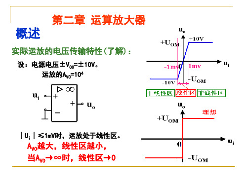
电子技术基础--第七章--集成运算放大器的线性应用和非线性应用

i1 i f 0
u O (1
Rf R1
)u i
u I 0 R1i1
uI i2 i1 R1
i1
uI R1
0 u M R2 i2
u M R2 i 2 R2 uI R1
0 u M R3i3
减法器的输出电压为两个输入信号之差乘以放大系数 Rf/R1, 故又称它为差分放大器。 为减小失调误差 R1//Rf=R2//R3
(五)反相积分运算电路
duC i 2 C dt
uC 0 uO
duo i2 C dt
u I 0 R1i1
i1 i2 0
du uI (C o ) 0 R1 dt
vI T
(同相过零比较器)
O
2
3
4
t
电压传输特性
vO
vO VOH
VOH O t
O VOL
vI
VOL
思考
1.若过零比较器如图所示,则它 的电压传输特性将是怎样的? 2.输入为正负对称的正弦波时, 输出波形是怎样的?
+VCC vI + A -VEE vO
vI T 2
+VCC vI + A -VEE vO
具体电路的工作原理,其它问题也就迎刃而解了。
比例运算电路 加法电路
减法电路 积分电路
微分电路
一、运算电路
• (一)反相比例运算电路 • (二)同相比例运算电路
(一)反相比例运算电路
i1 i f 0
u N uo R f i f
if u N uO u O Rf Rf
运算放大器介绍54页PPT
vI
R1
vN -
vP
A +
vO
AV= -(Rf / R1)= -20/10= -2
R2
Vo= AV Vi=(-2)(-1)=2V
2.3 基本线性运放电路
2.同相比例运算电路
Rf
虚断 v P = v I
0vN = vN vO
R1
Rf
R1
vN
-
vI
vP
A +
vO
虚短
vN = vP
vO
=
(1
Rf R1
= 2R6m'LVIEvX
IE
=
IC3 2
1 2
vy Re
vO =KvXvY
2.5 模拟乘法器电路
2、模拟乘法器符号 vO =KvXvY
K为比例因子,一般为正。
3、乘法运算
2.5 模拟乘法器电路
4、乘方和立方运算
2.5 模拟乘法器电路
5、除法运算
根据虚端虚断有:
-
v2 =Kvx2vO
+
Vo与vx1、vx2之商成比例,实现了除法运算 只有当vx2为正极性时,才能保证运放处于负反馈状态 vx1则可正可负
iCiEIESe VT
vO=VTlnvR S VTlnIES
其中,IES 是发射结反向饱和电流,vO是vS的对数运算。
2.4 基本运算电路
4. 反对数运算电路
利用虚短和虚断,电路有
iF
R
vS =vBE
vB E
iFiEIESe VT
vS
iE T
–
+
vO
vO =iFR
vS
vO =IESe VT
【精品】电子信息工程专业英语课后答案

电子信息工程专业英语课后答案电子信息工程专业英语-教师用书Part 1第一课关于电子技术一、课文习题参考答案Ⅰ. (1) alternating current circuits (2) semiconductor diodes(3) passive component(4) the combinatory logic electric circuit(5) rectification(6) Laplace transform(7) inductor(8) Fourier series and Fourier transformⅡ.(1)控制理论(2)场效应管三极管(3)布尔代数(4)稳压(5)相关性和功率谱密度(6)滤波器类型(7)模/数转换器(8)时序逻辑电路的分析与综合Ⅲ.(1)Electronics is a part of the larger field of electricity. The basic principles of electricity are also common to electronics. Modern advances in the field of computer, control system, communications have a close relationship with electronics. The field of electronics includes the electron tube, transistor, integrated circuit and so on.(2) Direct current circuits & Alternating current circuits,Analog electronics,Digital electronics,signal and systems,Circuit theory and design, Control theory, Microcontrollersystems,Computer programming for engineering applications.(3) This curriculum mainly introduces the characteristics of semiconductor devices in linear application scope.The content involved in semiconductor diodes (PN junction diodes, special purpose diodes), transistors (field effects and bipolar transistors), signal amplifiers, practical amplifiers, biasing circuits, operationalamplifiers circuit and other circuits (rectification, regulation and DC power supplies).(4) This partial studies take the basicelectric circuit theory and the operational amplifier knowledge as the foundation. The main study goal is to enhance understanding of the electric circuit theory. Its main content includes the elementary theory in circuit theory (network functions, characteristic frequencies), types offilter (lowpass,bandpass), review of operational amplifiers (design of first and second order using operational amplifiers, cascade design), filter characteristics(Butterworth, Chebyshev, frequency transformations in design, sensitivity design of passive LC ladder filters and a brief introduction to switched capacitor filters).(5) Perfect.二、参考译文电子学的发展电子学是电学的一部分。
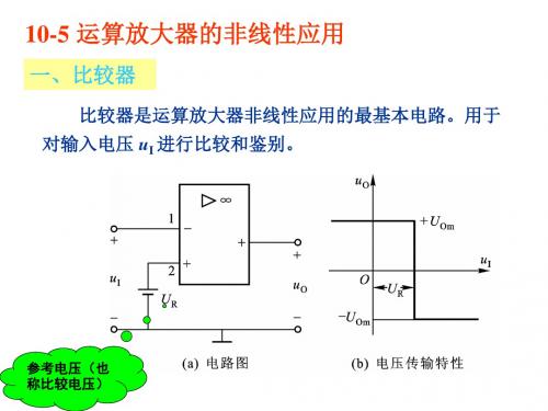
10-5 运算放大器的非线性应用
零迟滞比较器电路图
独立信号源方波发生器电路
方波发生器工作原理
⒈ uC=0至t=t1时的变化过程
从uO=+UOm开始讨论:
起初
v
u F
U RH
R
R 2
R
U Om ,uC不能跃变,v-=uC=0,由于R1上加
2
f
的电压uR1= + UOm-uC,C 将在+UOm作用下充电,等到uC≥URH时,v-≥v+,
电压,这种电路称为零比较器。
零比较器波 形图
2. 比较电压UR为一正值时 比较电压UR为一正值时,若ui为幅值大于UR的正弦波,
则输出电压uo的波形是与ui同频率但正负半周宽度不相等的 矩形波,幅值仍决定于运算放大器的最大输出电压。显然 改变UR的数值,可以改变其正负半周宽度的比例。
比较器 波形图
uF
uO1
uO2
uO1
t>t1后,C经R反向放电,
在 t = t2时,uO2= uC ,过零,C
uO2
开始经R正向充电,直到 t = t3
时,uO2
R 2
R
U Z ,uF过0,uO1立
刻翻转为+UZ1 。
R=R′时的uO1、uO2波形图
uF
uO1
uO2
uO1
在 t>t3后,C经R′正向放电,
直至在 t = t4,uO2= uC ,再次过
uO2
零,回到 t = 0的状态,完成一
次循环。
R=R′时的uo1、uo2波形图
uF
uO1
uO2
可见:
uO1
三角波的变化范围为:
R2 R
UZ
常用运放公式大全
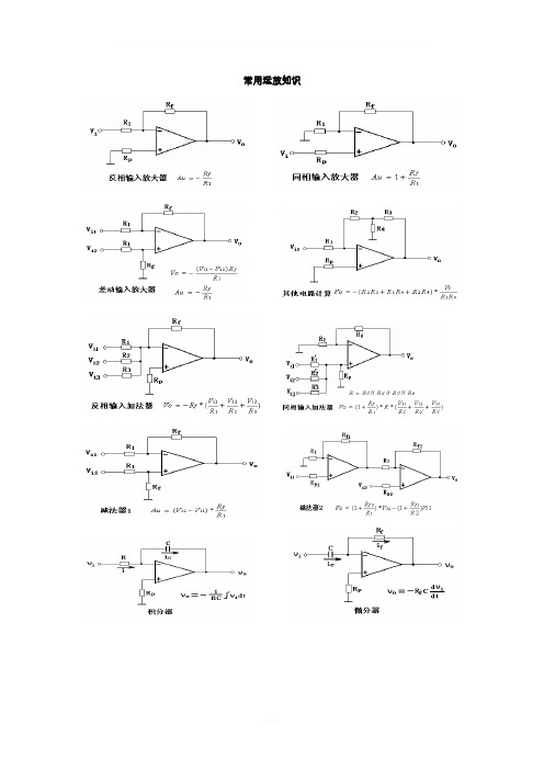
常用运放知识振荡器电路RC 有源滤波器1. 低通归一化传输函数: 一阶: 11)(+=S S H 二阶:1/1)(2++=Q S S S H (巴特沃兹:21=Q )2. 归一化低通 →去归一化变换(包括低通、高通、带通、带阻)一阶低通:0/011ωωω+−−→−+=s S s S二阶低通:200220/20111ωωωω++−−→−++=s Qs S Q S s S一阶高通:/011ωω+−−→−+=s s S s S二阶高通:2022/20111ωωω++−−→−++=s Qs s S Q S sS带通:2002)/)(/(20011ωωωωω++−−−−−→−+-=s Qs sQ S s s Q S带阻:2002202)//(/20011ωωωωω+++−−−−−→−++=s Qs s S s s Q S3. 滤波器电路和传输函数 一阶低通:)1()1(/1/1)(00RrR s Rr R sC R sCs H F F ++=++=ωωRC10=ω 一阶高通:)1()1(/1)(0RrR s s Rr R sC R R s H F F ++=++=ωRC10=ω 二阶滤波器的电路实现:通用传输函数:0120122)(a s a s b s b s b S H ++++=压控通用电路:二阶低通:通用传输函数:200220)/()(ωωω++=s Q s H s H1122221211221211)111()/()(C R C R C R A C R C R s s C C R R A s H F F +-+++=,与上式比较后得到: 2121201C C R R =ω Rr R A H F F +==10 221112211122)1(1C R CR A C R C R C R C R QF -++=设计方法:令R 1=R 2=R ,C 1=C 2=C ,则 RC 10=ωF A Q-=31或 Rr R Q A F F +=-=113元件值求解(f 0,Q 值已知)方法一:先固定C 1=C 2=C 为标称值,再根据 RC10=ω 求出R , 最后根据已知Q 值,由RrR Q A F F +=-=113 求出R F /Rr ; 方法二:取H 0=A F =1,即运放接成电压跟随器的形式,取R 1=R 2=R 为标称值,则2101C C R =ω,1221C C Q =,得出电容的计算公式:R Q C 012ω=R Q C 0221ω=二阶高通:通用传输函数:200220)/()(ωω++=s Q s s H s H1122112212221)111()(C R C R C R A C R C R s s s A s H F F +-+++= ,与上式比较后得到: 2121201C C R R =ω Rr R A H F F +==10 112222111221)1(1C R CR A C R C R C R C R QF -++=设计方法:令R 1=R 2=R ,C 1=C 2=C ,则RC10=ω Rr R A Q F F -=-=231 或 Rr R Q A F F +=-=113元件值求解(f 0,Q 值已知)方法一:先固定C 1=C 2=C 为标称值,再根据 RC10=ω 求出R , 最后根据已知Q 值,由RrR A Q F F -=-=231求出R F /Rr ; 方法二:取A F =1,1)(=∞H ,即运放接成电压跟随器的形式,取C 1=C 2=C 为标称值,则2101R R C =ω,2121R R Q =,得出电阻的计算公式: C Q R 0121ω= C Q R 022ω=二阶带通:通用传输函数:200200)/()/()(ωωω++=s Q s sQ H s H)11(1)11111()/()(213212221231211221R R R C C C R A C R C R C R C R s s C R sA s H F F ++-+++++=与上式比较后得到:)11(12132120R R R C C +=ω )1(1)(211221123100F FA R R C R C R C C R R A H H -++++==ω)]111()11([121321211221321R A R R C C R R C C R R R R R Q F-++++++=设计方法:令R 1=R 2=R 3=R ,C 1=C 2=C ,则RC 20=ω F F A A H -=5)(0ω)5(211F A Q -= 元件值求解(f 0,Q 值已知):先固定C 1=C 2=C 为标称值,通过以下公式求得其他元件:C R 02ω= ,Rr R Q A F F +=-=125 ,Q Rr R F 24-= ,125)(0-=Q H ω * 该电路的H(ω0)与Q 值有关,不能独立设计,如果必要,在确定Q 值之后,可嘉放大器或衰减器来调节H(ω0)。
运放-1-理想运放与虚断虚短的来源

今天开始,聊一聊运放吧,之前很多兄弟们也提了这个要求。
正好我最近也想深入看看运放方面的,那么就借这个机会一步一步再搞一搞吧。
运放这个器件相对于电阻,电容,三极管,MOS管等器件算是比较复杂的,而且电路中也常用,出问题的情况也多,显然一篇文章根本就说不明白运放,因此,我可能要写很多期。
具体多少期,写哪些内容,我一向都是不做计划,随心所欲,兄弟们有需求也可以提,我可以看情况安排。
背景介绍完了,那么就开始了。
第一步,理想运放首先,第一个问题,我为什么要说理想运放呢?因为一般来说,我们了解一个东西,都是先将它当做理想来看的,这样最为简单,也最容易懂。
当我们拿到一个陌生的电路,首先我们肯定是要知道这个电路是干什么用的对不?这个时候我们就先不用考虑电路中器件的非理想特性,比如先不考虑温漂,漏电,寄生电感,寄生电容等等这些。
我们就先把它当做理想的,然后看这个电路到底实现了什么功能,运放电路一般也是这么分析的。
等我们知道这个电路是干啥用的,然后再看看器件的哪些特性会导致这个电路失效,或者说不按照预期的工作,这个时候就要考虑非理想特性了。
所以,我们了解理想运放的目的,就是为了在一开始的时候能快速的分析出电路的工作原理,实现了什么功能。
其次,理想运放有哪些特性呢?理想运放主要有以下三点:1、增益无穷大2、输入阻抗无穷大3、输出阻抗为0那么这三点特性又是怎么来的呢?1、增益无穷大增益无穷大好理解,因为一般运放的增益就是很大的,比如Ti的uA741,开环增益是105dB左右,计算一下是多少倍呢?20log(Av)=105dB,计算得Av=10^5.25=177828,大约是18万倍。
相对于我们一般电路中几十倍的放大倍数,这个很大了。
2、输入阻抗无穷大理想运放的输入阻抗无穷大,我们看看实际运放的,还是以Ti的uA741为例,如下图:可以看到,输入阻抗还是比较大的,典型值是2MΩ,其实这个芯片在运放中阻抗算是偏小的了。
比如TI的另外一款芯片LM358的输入阻抗就更大,差分输入阻抗10MΩ,共模输入阻抗4GΩ。
运算放大器公式
运算放大器公式
在电路设计中,运算放大器是一种重要的基础电路元件。
它被广泛应用于信号放大、滤波、积分、微分、比较、反相器、非反相器等电路中。
下面是几个常用运算放大器公式:
1. 增益公式
运算放大器的增益可以用下面的公式计算:
A = -Rf/Rin
其中,A表示增益,Rf表示反馈电阻,Rin表示输入电阻。
2. 反相放大器公式
反相放大器是一种常用的基础电路,它的输入信号经过放大后会被反相输出。
反相放大器的放大倍数可以用下面的公式计算:
Vout = -Vin * Rf/Rin
其中,Vin表示输入电压,Vout表示输出电压,Rf表示反馈电阻,Rin表示输入电阻。
3. 非反相放大器公式
非反相放大器可以将输入信号放大后,保持输出信号与输入信号同相。
非反相放大器的放大倍数可以用下面的公式计算:
Vout = Vin * (1 + Rf/Rin)
其中,Vin表示输入电压,Vout表示输出电压,Rf表示反馈电阻,Rin表示输入电阻。
以上是几个常用运算放大器公式,它们在电路设计中都有重要的应用。
在实际设计中,我们可以根据具体情况选择合适的公式来计算
电路参数,以实现设计要求。
运放的非线性应用 电路知识讲解

滞回电压比较器(9)
例题:R1=10k,R2=10k ,UZ=6V, UR=10V。当 输入ui为如图所示的波形时,画 出输出uo的波形。
上下限:
R1 R2 U th1 UZ U R 8V R1 R 2 R1 R 2 R1 R2 U th 2 UZ U R 3V R1 R 2 R1 R 2
解决措施
采用滞回 比较器
干扰引起系 统误动作
反相滞回比较器
ui
R1
结构特点:
运放工作于正反馈状态
比较信号加入反相输入端
UR R2
Δ ∞ + +
u0
分析过程: +UOM 第一步: 由运放非线性工 u = o 作特点,有 -UOM 第二步: 由电路求u+与u(1) 对图示电路,有 u-=ui (2) 用叠加原理求u+
运放工作在非线性状态的条件运放非线性应用的条件与特点2运放工作在非线性状态下的两个特点om为运放为运放输出的正负最大值为运放同相与反相端的输入电流因为对于理想运放有rid所以end注意
模拟信号比较电路
运放非线性应用的条件和分析特点
单限电压比较器 滞回电压比较器
运放非线性应用的条件与特点(1)
+U
运放工作在非线性状态的条件
R1 R2
± UZ
(1) 阈值计算 对图示电路,有 用叠加原理求u+
u-=UR
uo单独作用 ui单独作用
R1 R2 U ( U Z ) ui R1 R2 R1 R2
注意:对于不同的输出值,U+有两个取值
滞回电压比较器(7) U
当uo=-UZ时,
U 1
R3
R
运算放大器的线性应用和非线性应用PPT文档共57页

6、法律的基础有两个,而且只有两个……公平和实用。——伯克 7、有两种和平的暴力,那就是法律和礼节。——歌德
8、法律就是秩序,有好的法律才有好的秩序。——亚里士多德 9、上帝把法律和公平凑合在一起,可是人类却把它拆开。——查·科尔顿 10、一切法律都是无用的,因为好人用不着它们,而坏人又不远躺在泥坑里的人,才不会再掉进坑里。——黑格尔 32、希望的灯一旦熄灭,生活刹那间变成了一片黑暗。——普列姆昌德 33、希望是人生的乳母。——科策布 34、形成天才的决定因素应该是勤奋。——郭沫若 35、学到很多东西的诀窍,就是一下子不要学很多。——洛克
常用运放公式大全

常用运放公式大全运放(Operational Amplifier,OP)是一种重要的电子元器件,广泛应用于模拟电路中。
运放可以放大电压信号、实现各种线性运算以及滤波、比较等功能。
在设计和分析电路时,常用的运放公式非常有用,下面是一些常用的运放公式。
1.运放的基本理想模型公式:Vout = A*(V+ - V-),其中Vout为运放的输出电压,A为运放的放大倍数,V+和V-分别为非反馈输入和反馈输入的电压。
2.反向放大运放电压放大倍数公式:Vout = -Rf/Ri * Vin,其中Rf为反馈电阻,Ri为输入电阻,Vin为输入电压。
3.非反向放大运放电压放大倍数公式:Vout = (1 + Rf/Ri) * Vin,其中Rf为反馈电阻,Ri为输入电阻,Vin为输入电压。
4. 电压跟随器(Voltage Follower)电压放大倍数公式:Vout ≈ Vin,电压跟随器的输入电压和输出电压近似相等。
当V+ > V-时,Vout = Vsat+,当V+ < V-时,Vout = Vsat-。
Vsat+和Vsat-分别为正饱和电压和负饱和电压。
CMRR = 20 * log10(Aac/Acm),其中Aac为差模增益,Acm为共模增益。
7. 运放的输入偏置电流(Input Bias Current)公式:输入偏置电流为非反馈输入端和反馈输入端的电流之差。
8. 极限频率(Gain Bandwidth Product,GBP)公式:GBP=A*f,其中A为运放的放大倍数,f为运放的截止频率。
9. 运放的输入偏置电压(Input Offset Voltage)公式:输入偏置电压为非反馈输入端和反馈输入端的电压之差。
10.运放的输入阻抗公式:输入阻抗可以用输入电阻(Ri)和输入电流(Ii)表示,输入阻抗Zi=Ri+(1/A)*Ri。
11.运放的输出阻抗公式:输出阻抗可以用输出电阻(Ro)和输出电流(Io)表示,输出阻抗Zo=Ro+(1/A)*Ro。
运算放大器应用思考题和习题

1. 理想集成运放的=________,=________,=________,ud A id r 0r B I =________,CMRR=________2. 理想集成运放工作在线性区和非线性区时各有什么特点?各得出什么重要关系式3. 集成运放应用于信号运算时工作在什么区域?4. 试比较反相输入比例运算放大电路和同相输入比例运算电路的特点(如闭环电压放大倍数、输入电阻、共模输入信号、负反馈组态等)5. 虚地的实质是什么?为什么虚地的电位接近0而又不等于0?在什么情况下才能引用虚地的概念?6. 为什么用集成运放组成的多输入运算电路,一般多采用反相输入的形式,而较少采用同相输入的形式? 7. 反相比例电路如图7-43所示,图中i R =10K Ω,f R =30K Ω,试估算它的电压放大倍数和输入电阻,并估算1R 应取多大?8. 同相比例运算电路如图7-44所示,图中i R =3K Ω,若希望它的电压放大倍数等于7,试估算电阻f R 和1R 的值9. 电路如图7-44所示,如集成运放的最大输出电压为±12V ,电阻1R =10K Ω,f R =390K Ω,1R =1R //f R ,输入电压等于0.2V ,试求下列各种情况下的输出电压值。
(1) 正常值 (2) 电阻1R 开路 (3) 电阻f R 开路10.试根据下列要求,设计比例放大电路(1) 设计一个电压放大倍数为-5,输入电阻为100K Ω的放大电路 (2) 设计一个电压放大倍数为-20,输入电阻为2K Ω的放大电路 (3) 设计一个输入电阻极大,电压放大倍数为+100的放大电路11.集成运放电路如图7-45所示,它们均可将输入电流转换为输出电压,试分别估算它们在i I =5A μ时的输出电压12.电路如图7-46所示,图中集成运放均为理想集成运放,试分别求出它们的输出电压与输入电压的函数关系;输入电阻;指出哪些符合“虚地”;指出哪些电路对集成运放的共模抑制比不高13.电路如图7-47所示,集成运放均为理想集成运放,试列出它们的输出电压,,的表达式o U 1o U 2o U14.电路如图7-48所示,集成运放均为理想集成运放,试写出电路输出电压的表达式15.试用集成运算放大器实现以下求和运算 (1)=-() o U 12102i i U U U ++3i 3i (2)=o U 121.550.1i i U U U −+而且要求对应于各个输入信号来说,电路的输入电阻不小于5K Ω。
2.4-非线性电路方程
u4 = 50 0.01+ 0.5 (0.01)3 50 i4
的 形 成 — 非 线 性 电 路 方 程
u1=100+0.58=104V
i3=10A i4=0.010A
①非线性电阻能产生与输入信号不同的频率(谐波污染)。 ②非线性电阻工作范围充分小时,可用工作点处的线性 电阻来近似。 ③齐次性和叠加性不适用于非线性元件。
2.4 非线性电路
2.4
2.4.1 非线性元件
二极管、三极管、电力电子器件等属于非 线性器件,对于非线性器件,可以用含有线 性元件、非线性元件的模型来等效,至少包 含一个非线性元件的电路称为非线性电路 (nonlinear circuit)。 非线性元件有时变和非时变之分,这里, 仅介绍非时变的非线性电阻、非线性电容、非 线性电感元件的基本概念。
齐次性和叠加性不适用于非线性元件 i1=2 A, i3=10A, u1=104V u3=1000V 齐次性不满足
2.4
当 i = i1 + i2 ( 迭加 )
u =f (i) =50 i + 0.5
u =50(i1 + i2)+0.5(i1 + i2)3 =50 i1+ 0.5 i13 + 50 i2 +0.5 i2 3 +1.5 i1i2(i1 + i2) = u1 + u2 +1.5 i1i2(i1 + i2) u1 + u2 迭加性不满足
性 电 路 方 程
电 路 方 程 的 形 成 —
u
u= f (i) = a0i + a1
i2 +
- 1、下载文档前请自行甄别文档内容的完整性,平台不提供额外的编辑、内容补充、找答案等附加服务。
- 2、"仅部分预览"的文档,不可在线预览部分如存在完整性等问题,可反馈申请退款(可完整预览的文档不适用该条件!)。
- 3、如文档侵犯您的权益,请联系客服反馈,我们会尽快为您处理(人工客服工作时间:9:00-18:30)。
南京理工大学泰州科技学院毕业设计(论文)外文资料翻译学院 (系): 电子电气工程学院专 业: 电子信息工程姓 名: 张 国 彬学 号: 0802040149外文出处: Development of the Nonldeal Op Amp Equations附 件:1.外文资料翻译译文;2.外文原文。
注:请将该封面与附件装订成册。
指导教师评语: 签名: 年 月 日 (用外文写)附件1:外文资料翻译译文非理想运算放大器方程的导出1.引言运放中的误差来源有两类,用一般的分类方法可以分为DC误差(直流误差)和AC误差(交流误差)。
DC误差的例子有输入失调电压和输入偏置电流。
DC 误差在运算放大器可使用的频率范围内是保持恒定的。
因此,输入偏置电流在1kHz 下是l0pA,在10KHz下也是l0pA。
由于DC误差具有恒定和可控的性质,所以对它们的讨论我们将会到后面再继续进行。
AC误差是易变的。
我们在这里对AC误差进行分析的方法,是导出一组考虑到AC误差的非理想方程。
AC误差可以在DC状态下出现,但随着工作频率的增加,AC误差会变得越来越糟。
AC误差的一个很好的例子是CMRR(Common Mode Rejection Ratio,共模抑制比)。
大多数远放都有一个确保的CMRR指标,但这个指标只在DC或非常低的频率下才有效。
当我们进一步阅读数据手册时,我们就可以发现CMRR会随着工作频率的增加而下降。
归入AC误差的其他几个指标有输出阻抗.、电源抑制比、峰到峰输出电压、差分增益、差分相位和相位裕度等。
差分增益是最重要的AC 指标,因为其他的AC指标都是由差分增益导出的。
在前面,我们一直把差分增益叫做运放增益或运放开坏增益,我们将继续使用这些术语。
在数据手册中,这个术语叫做差分增益。
正如前面几章中所说的,当频率增加时,运放的增益就降低,误差就增加。
这一章将导出几个方程,用以说明增益的改变所产生的这些影响。
我们将首先回顾基本典范反馈系统的稳定性,因为运放方程的导出使用了相同的技术。
放大器是用像晶体管这样的有源元件构建的。
而晶体管的主要参数,比如晶体管的增益,是易于漂移的,此外,来自许多不同制造商的元件都存在初始的不精确性,因此,用这些元件构建的运放同样易于漂移和不精确。
不过,这种漂移和不精确可以通过使用负反馈而得以减小甚至消除。
运放电路就是采用了这种反馈的结构,使电路的传递方程与放大器本身的参数无关(几乎完全无关),而只取决于外部无源元件。
外部无源元件可以采购成满足几乎任何漂移或精度的要求,限制这些无源元件使用的只是它们的成本和体积。
运放一旦加有反馈,运放电路就可能变为不稳定。
有些放大器属于一种叫做内部补偿运放的类别,这些运放包含了一些有时被广告里说成可以避免不稳定的内部电容。
虽然工作在指定条件下的内部补偿运放是不应该振荡的,但也有许多这样的电路仍然会有相对的不稳定性,这说明这些电路本身存在着很差的相位响应和易于产生振铃与过冲的问题。
唯一绝对稳定的内部补偿运放只是那种躺在实验台上且未加电源的运放!所有其他的内部补偿运放都会在某些外部电路条件下产生振荡。
非内部补偿或者外部补偿的运放,在没有加上起稳定作用的外部元件时,是不稳定的。
这种情况对许多应用是个缺点,因为这些运放需要增加额外的元件。
然而,没有内部补偿的运放可以使高明的电路设计者完全地发挥出运放的全部性能。
于是,设计者面临两种选择:采用已由IC 制造商做了内部补偿的运放,或者由设计者自己对运放做外部补偿。
除了由运放制造商做好补偿之外,其他的运放都必须在IC 外面做补偿。
非常有意思的是,为了满足要求很高的应用,内部补偿的运放也还需要进行外部补偿。
补偿是通过增加外部元件以修改电路的传递函数来实现的,并以此使电路变成无条件稳定。
对运放进行补偿有几种不同的方法,每种补偿方法都有它的优点和缺点。
我们必须对补偿以后的运放电路进行分析,以确定补偿的效果。
此外,根据补偿对于闭环传递函数的改善效果,往往可以确定出哪种补偿她会有最大的收效。
2.典范方程的回顾输出方程和误差方程重复如下(6-1) (6-2) 由上面的两个方程经过代入法后可以得到下面的(6-3)方程:(6-3) 然后合并同类项之后又可以得到得到(6-4)的方程: IN OUT V A V =+⎪⎪⎭⎫⎝⎛β1 (6-4) OUT IN OUT V V E EAV β-==OUT IN OUT V V A V β-=把上述方程各项经过整理之后,可以得到反馈方程的经典形式(6-5)的方程: (6-5)由上面我们可以看出,当式(6-5) 中的量Aβ变成相对于1 非常大的时候.式(6-5) 即简化为式(6-6)。
式 (6-6) 叫做理想反馈方程.因为它取决于假设Aβ>> 1。
当放大器被认为具有理想品质的时候, 这个方程有着广泛的用途.在Aβ>> 1 的条件下,系统增益将由反愤因子β确定。
我们是用稳定的无源元件来实现这个反馈因子的,因此,理想的闭环增益是可预测的和稳定的,因为β是可预测的和稳定的。
β1=IN OUT V V (6-6) 可以看出Aβ这个量非常重要,因此我们给了它一个特殊的名称:环路增益。
我们来考察图6-2,在把输入电压接地(若电流输入则是断开)和把环路断开之后,所计算出的增益就是环路增益Aβ。
这里需要注意的是,这是一些复数运算,复数有幅度和方向。
当环路增益趋于-1 或者用数学式表示为1角-180度。
的时候,式 (7-5) 就趋于无穷大,因为1/0=>∞。
这时,电路的输出将沿着一条直线方程、以尽可能快的速度奔向无穷大。
如果输出不受能量限制,这个电路将摧毁整个世界,好在电路的能量受到电源的限制,所以,这个世界丝毫米损。
当电路输出趋于电源电压时,电路中的有源器件会表现出非线性,而这种非线性降低了放大器的增益,使环路增益不再等于1 角-180度。
现在,电路可以做两件事:第一,电路可以稳定在电源的一个端电压上,第二,电路可以改变方向(因为存储的电荷会使输出电压继续改变),奔向电源的另一端。
在第一种情况下,也路稳定在电源的一个端电压上,这叫做锁定。
电路将一直保持在这个锁定状态,直到电源被切断。
在第二种情况下,电路在电源的两个端电压之间来回跳动,这叫做振荡。
我们应该知道,环路增益Ass 是唯一一个确定电路或系统稳定性的因子。
当计算环路增益时,首先要把输入接地或断开,因为输入不会对稳定性有任何影响。
我们将在后面对环路增益这个判别准则进行深入分析。
把式(6-1)和式(6-2)合并和整理之后,可以得到式(6-7) ,这个等式给出了系统βA A V V IN OUT +=1或电路的误差:βA V E IN +=1 (6-7) 首先可以看出,误差是与输入信号成正比的。
这是所期望的结果,因为较大的输入信号产生较大的输出信号,而较大的输出信号需要较大的驱动电压。
其次,环路增益与误差成反比误差会随环路增益的增加而减小.因此,大的环路增益对于减小误差是很有用的. 但大得环路增益同时也降低了稳定性.所以,在误差和稳定性之间总是存在折中关系。
3.同相运算放大器放大器传输过程的方程()B IN OUT V V a V -= (6-8) 同相运放的输出方程可以利用分压器规则导出.在使用分伍德规则的时候,我们实际上假设运放的输出阻扰很低。
0=+=B GF G OUT B forl Z Z Z V V (6-9) 结合上述两个方程我们就可以得到以下的方程 F G OUT G IN OUT Z Z V aZ aV V +-= (6-10) 对式(6- 10) 整理之后,我们又可以得到式 (6-11 ),可以得出了这个同相电路的传递函数:FG G IN OUT Z Z aZ a V V ++=1 (6-11) 我们把式(6-5)重写一遍,编号为式 (6-12)以便子比较两个等式中的对应项: βA A V V IN OUT +=1 (6-12) 通过对式 (6-11)与式(6-12)的比较,可以得到式(6- 13),这是同相运放的环路增益方程。
这个环路增益方程确定了电路的稳定性。
此外,上面的比较还指出了同相电路的开环增益A 就是运放的开环增益a 。
(6-13) F G GZ Z aZ A +=β把测试电压TEST V 乘以运算放大器开环增益后,获得运放的输出电压TEST aV 。
然后用分压器规则得到式子(6-14)。
然后对(6-14)进行一些数据处理,得到(6-15)。
这是同相运放的环路增益。
而且与(6-13)完全是一样的。
(6-14) (6-15)4.反相功放电路的传递方程A OUT aV V -= (6-16)式 (6-17) 中的节点电压方程是利用叠加定理和分压器规则得到的.式 (6-18) 是利用式(6-16) 和式 (6-17) 得出的。
(6-17) (6-18)式 (6-18) 是反相运放的传递函数。
通过对式(6-18) 与式 (6-12) 的比较,我们又得到了式 (6-13) .而这也是图6-5 中反相运放电路的环路增益方程.通过比较还可以知道,反相电路的开环增益A 是与同相电路的运放开环增益a 不同的。
我们把反馈环路断开后的反相运放回示图6-6 中,这个电路可以用来导出式 (7-19)中的环路增益:(6-19)分析到这里,我们必须对几件事做一说明。
首先,式 (6-11)和式 (6-18) 中的同相和反相方程的传递值数是不同的.对于同样的一组G Z 和F Z 值,无论增益的大小还是极性都是不同的.其次,两个电路的环路增益悬完全一样的,这就是式 (6-13) 和式 (6-19)。
因此,这两个电路在稳定性方面的特性也是完全相同的,虽然两者的传递方程是不同的.这就得出了一个重要的结论:稳定,蚀与电路的输入无关。
最后,图6-1中的增益框A 。
, 对于每一个运放电路都是不同的.通过对式F G G F G F IN OUTB F G G OUT F G F IN A Z Z aZ Z Z aZ V V forl Z Z Z V Z Z Z V V +++-==+++=10G F G TEST RETURNG F G TEST RETURN Z Z aZ A V V Z Z Z aV V +==+=ββA Z Z aZ V V F G G TEST RETUNRN =+=(6-5)、式 (6-11) 和式 (6-18) 的比较.可以看出,同相时a A INV NON =-,反相时()F G F INV Z Z aZ A +=。
附件2:外文原文Development of the Nonldeal Op Amp Equations6.1IntroductionThere are two types of error sources in op amps, and they fall under the general classification of dc and ac errors. Examples of dc errors are input offset voltage and input bias cur- rent. The dc errors stay constant over the usable op amp frequency range; therefore, the input bias current is 10 p A at 1 kHz and it is 10 pA at 10 kHz. Because of their constant and controlled behavior, dc errors are not considered until later chapters.AC errors are flighty, so we address them here by developing a set of nonideal equations that account for ac errors. The ac errors may show up under dc conditions, but they get worse as the operating frequency increases. A good example of an ac error is common– mode rejection ration (CMRR). Most op amps have a guaranteed CMRR specification, but this specification is only valid at dc or very low frequencies. Further inspection of the data sheet reveals that CMRR decreases as operating frequency increases. Several other specifications that fall into the category of ac specifications are output impedance, power-supply rejection-ratio, peak-to-peak output voltage, differential gain, differential phase, and phase margin.Differential gain is the most important ac specification because the other ac specifications are derived from the differential gain. Until now, differential gain has been called op amp gain or op amp open loop gain, and we shall continue with that terminology. Let the data sheet call it differential gain.As shown in prior chapters, when frequency increases, the op amp gain decreases and errors increase. This chapter develops the equations that illustrate the effects of the gain changes. We start with a review of the basic canonical feedback system stability because the op amp equations are developed using the same techniques.Amplifiers are built with active components such as transistors. Pertinent transistor parameters like transistor gain are subject to drift and initial inaccuracies from many sources, so amplifiers being built from these components are subject todrift and inaccuracies. The drift and inaccuracy is minimized or eliminated by using negative feedback. The op amp circuit configuration employs feedback to make the transfer equation of the circuit independent of the amplifier parameters (well almost), and while doing this, the circuit transfer function is made dependent on external passive components. The external pas- sive components can be purchased to meet almost any drift or accuracy specification; only the cost and size of the passive components limit their use.Once feedback is applied to the op amp it is possible for the op amp circuit to become unstable. Certain amplifiers belong to a family called internally compensated op amps; they contain internal capacitors that are sometimes advertised as precluding instabilities. Although internally compensated op amps should not oscillate when operated under specified conditions, many have relative stability problems that manifest themselves as poor phase response, ringing, and overshoot. The only absolutely stable internally compensated op amp is the one lying on the workbench without power applied! All other internally compensated op amps oscillate under some external circuit conditions.Non internally compensated or externally compensated op amps are unstable without the addition of external stabilizing components. This situation is a disadvantage in many cases because they require additional components, but the lack of internal compensation enables the top drawer circuit designer to squeeze the last drop of performance from the op amp. You have two options: op amps internally compensated by the IC manufacturer, or op amps externally compensated by you. Compensation, except that done by the op amp manufacturer, must be done external to the IC. Surprisingly enough, internally compensated op amps require external compensation for demanding applications.Compensation is achieved by adding external components that modify the circuit transfer function so that it becomes unconditionally stable. There are several different methods of compensating an op amp, and as you might suspect, there are pros and cons associated with each method of compensation. After the op amp circuit is compensated,it must be analyzed to determine the effects of compensation. The modifications that compensation have on the closed loop transfer function often determine which compensation scheme is most profitably employed.6.2Review of the Canonical EquationsA block diagram for a generalized feedback system is repeated in Figure 6–1. This simple block diagram is sufficient to determine the stability of any system.The output and error equation development is repeated below. (6-1) (6-2)Combining Equations 6–1 and 6–2 yields Equation 6–3 IN OUT V AV =+⎪⎪⎭⎫ ⎝⎛β1 (6-3) Collecting terms yields Equation 6–4: (6-4)Rearranging terms yields the classic form of the feedback equation.(6-5)Notice that Equation 6–5 reduces to Equation 6–6 when the quantity Ain Equation 6–5 becomes very large with respect to one. Equation 6–6 is called the ideal feedback equation because it depends on the assumption that A>> 1, and it finds extensive use when amplifiers are assumed to have ideal qualities. Under the conditions that A>>1, the system gain is determined by the feedback factor Stable passive circuit components are used to implement the feedback factor, thus the ideal closed loop gain is predictable and stable because is predictable and stable.β1=IN OUT V V (6-6) The quantity A is so important that it has been given a special name, loop gain. Consider Figure 6–2; when the voltage inputs are grounded (current inputs are opened) OUT IN OUT V V E EAV β-==OUT IN OUT V V A V β-=βA A V V IN OUT +=1and the loop is broken, the calculated gain is the loop gain, A Now, keep in mind that this is a mathematics of complex numbers, which have magnitude and direction. When the loop gain approaches minus one, or to express it mathematically 1–180 , Equation 6–5 approaches infinity because 1/0 . The circuit output heads for infinity as fast as it can using the equation of a straight line. If the output were not energy limited the circuit would explode the world, but it is energy limited by the power supplies so the world stays intact.Active devices in electronic circuits exhibit nonlinear behavior when their output ap- proaches a power supply rail, and the nonlinearity reduces the amplifier gain until the loop gain no longer equals 1 –180 . Now the circuit can do two things: first, it could become stable at the power supply limit, or second, it can reverse direction (because stored charge keeps the output voltage changing) and head for the negative power supply rail.The first state where the circuit becomes stable at a power supply limit is named lockup; the circuit will remain in the locked up state until power is removed. The second state where the circuit bounces between power supply limits is named oscillatory. Remember, the loop gain, A , is the sole factor that determines stability for a circuit or system. Inputs are grounded or disconnected when the loop gain is calculated, so they have no effect on stability. The loop gain criteria is analyzed in depth later.Equations 6–1 and 6–2 are combined and rearranged to yield Equation 6–7, which gives an indication of system or circuit error.βA V E IN +=1 (6-7) First, notice that the error is proportional to the input signal. This is the expected result because a bigger input signal results in a bigger output signal, and bigger output signals require more drive voltage. Second, the loop gain is inversely proportional to the error. As the loop gain increases the error decreases, thus large loop gains are attractive for minimizing errors. Large loop gains also decrease stability, thus there is always a trade off between error and stability.6.3 Non inverting Op AmpsA non inverting op amp is shown in Figure 6–3. The dummy variable, VB, is inserted to make the calculations easier and a is the op amp gain.Equation 6–8 is the amplifier transfer equation.()B IN OUT V V a V -= (6-8) The output equation is developed with the aid of the voltage divider ing the voltage divider rule assumes that the op amp impedance is low.0=+=B GF G OUT B forl Z Z Z V V (6-9) Combining Equations 6–8 and 6–9 yields Equation 6–10. F G OUT G IN OUT Z Z V aZ aV V +-= (6-10) Rearranging terms in Equation 6–10 yields Equation 6–11, which describes the transfer function of the circuit.FG GIN OUT Z Z aZ a V V ++=1 (6-11) Equation 6–5 is repeated as Equation 6–12 to make a term by term comparison of the equations easy .βA A V V IN OUT +=1 (6-12) By virtue of the comparison we get Equation 6–13, which is the loop-gain equation for the non inverting op amp. The loop-gain equation determines the stability of the circuit. The comparison also shows that the open loop gain, A, is equal to the op amp open loop gain, a, for the non inverting parison also shows that the open loop gain, A, is equal to the op amp open loop gain, a, for the non inverting circuit.(6-13) The test voltage, V TEST , is multiplied by the op amp open loop gain to obtain the op amp output voltage, a V TEST . The voltage divider rule is used to calculate Equation 6–15, which is identical to Equation 6–14 after some algebraic manipulation.F G G Z Z aZ A +=β(6-14) (6-15) The transfer equation is given in Equation 6–16:A OUT aV V -= (6-16) The node voltage (Equation 6–17) is obtained with the aid of superposition and the volt- age divider rule. Equation 6–18 is obtained by combining Equations 6–16 and 6–17.(6-17) (6-18)Equation 6–16 is the transfer function of the inverting op amp. By virtue of the comparison between Equations 6–18 and 6–14, we get Equation 6–15 again, which is also the loop gain equation for the inverting op amp circuit. The comparison also shows that the open loop gain (A) is different from the op amp open loop gain (a) for the non inverting circuit.The inverting op amp with the feedback loop broken is shown in Figure 6–6, and this circuit is used to calculate the loop-gain given in Equation 6–19.(6-19)Several things must be mentioned at this point in the analysis. First, the transfer functions for the non inverting and inverting Equations, 6–13 and 6–18, are different. For a common set of ZG and ZF values, the magnitude and polarity of the gains are different. Second,The loop gain of both circuits, as given by Equations 6–15 and 6–19, is identical. G F G TEST RETURNG F G TEST RETURN Z Z aZ A V V Z Z Z aV V +==+=βF G G F G F IN OUTB F G G OUT F G F IN A Z Z aZ Z Z aZ V V forl Z Z Z V Z Z Z V V +++-==+++=10βA Z Z aZ V V F G G TEST RETUNRN =+=Thus,the stability performance of both circuits is identical although their transfer equations are different. This makes the important point that stability is not dependent on the circuit in- puts. Third, the A gain block shown in Figure 6–1 is different for each op amp circuit. By comparison of Equations 6–5, 6–11, and 6–18 we see thataA INVNON=-and()FGFINV ZZaZA+=.。