A Worst Case Timing Analysis Technique for Multiple-Issue Machines
工艺角 corner
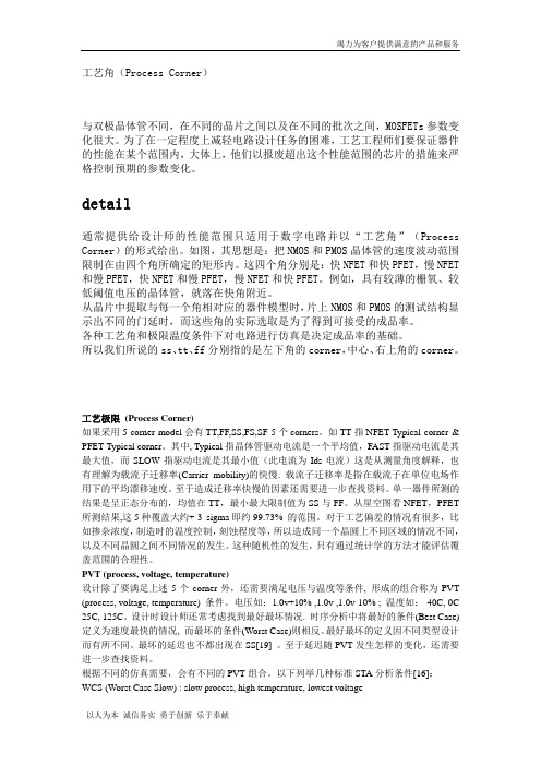
工艺角(Process Corner)与双极晶体管不同,在不同的晶片之间以及在不同的批次之间,MOSFETs参数变化很大。
为了在一定程度上减轻电路设计任务的困难,工艺工程师们要保证器件的性能在某个范围内,大体上,他们以报废超出这个性能范围的芯片的措施来严格控制预期的参数变化。
detail通常提供给设计师的性能范围只适用于数字电路并以“工艺角”(Process Corner)的形式给出。
如图,其思想是:把NMOS和PMOS晶体管的速度波动范围限制在由四个角所确定的矩形内。
这四个角分别是:快NFET和快PFET,慢NFET 和慢PFET,快NFET和慢PFET,慢NFET和快PFET。
例如,具有较薄的栅氧、较低阈值电压的晶体管,就落在快角附近。
从晶片中提取与每一个角相对应的器件模型时,片上NMOS和PMOS的测试结构显示出不同的门延时,而这些角的实际选取是为了得到可接受的成品率。
各种工艺角和极限温度条件下对电路进行仿真是决定成品率的基础。
所以我们所说的ss、tt、ff分别指的是左下角的corner,中心、右上角的corner。
工艺极限(Process Corner)如果采用5-corner model会有TT,FF,SS,FS,SF 5个corners。
如TT指NFET-Typical corner & PFET-Typical corner。
其中, Typical指晶体管驱动电流是一个平均值,FAST指驱动电流是其最大值,而SLOW指驱动电流是其最小值(此电流为Ids电流)这是从测量角度解释,也有理解为载流子迁移率(Carrier mobility)的快慢. 载流子迁移率是指在载流子在单位电场作用下的平均漂移速度。
至于造成迁移率快慢的因素还需要进一步查找资料。
单一器件所测的结果是呈正态分布的,均值在TT,最小最大限制值为SS与FF。
从星空图看NFET,PFET 所测结果,这5种覆盖大约+-3 sigma即约99.73% 的范围。
PSPICE仿真讲解学习

P S P I C E仿真目录介绍: (3)新建PSpice仿真 (4)新建项目 (4)放置元器件并连接 (4)生成网表 (6)指定分析和仿真类型 (7)Simulation Profile设置: (8)开始仿真 (8)参量扫描 (11)Pspice模型相关 (13)PSpice模型选择 (13)查看PSpice模型 (13)PSpice模型的建立 (14)介绍:PSpice是一种强大的通用模拟混合模式电路仿真器,可以用于验证电路设计并且预知电路行为,这对于集成电路特别重要。
PSpice可以进行各种类型的电路分析。
最重要的有:●非线性直流分析:计算直流传递曲线。
●非线性瞬态和傅里叶分析:在打信号时计算作为时间函数的电压和电流;傅里叶分析给出频谱。
●线性交流分析:计算作为频率函数的输出,并产生波特图。
●噪声分析●参量分析●蒙特卡洛分析PSpice有标准元件的模拟和数字电路库(例如:NAND,NOR,触发器,多选器,FPGA,PLDs和许多数字元件)分析都可以在不同温度下进行。
默认温度为300K电路可以包含下面的元件:●Independent and dependent voltage and current sources 独立和非独立的电压、电流源●Resistors 电阻●Capacitors 电容●Inductors 电感●Mutual inductors 互感器●Transmission lines 传输线●Operational amplifiers 运算放大器●Switches 开关●Diodes 二极管●Bipolar transistors 双极型晶体管●MOS transistors 金属氧化物场效应晶体管●JFET 结型场效应晶体管●MESFET 金属半导体场效应晶体管●Digital gates 数字门●其他元件 (见用户手册)。
新建PSpice仿真新建项目如图 1所示,打开OrCAD Capture CIS Lite Edition,创建新项目:File > New > project。
03-PSPICE仿真 (1)
23
模型参数
24
加元器件库(Place/Part命令)
在画电路图之前,首先要为将要画的电路选择元器件库。执行 Place/Part命令,,在Place/Part对话框中点击“Add”按钮,出现 Browse File对话框,将所需库点中,点击“打开”按钮,则选中的 库文件增至“Labrarise”框 中。反之,从“Labrarise”框,选中一 个库文件,点击Remove按钮,即将该库文件框剔除。
1/TSTOP
VAMPL
FREP TD DF PHASE
振幅
频率 延迟时间 阻尼系数 相位延迟
V
Hz s 1/s 度
FREQ=1kHz,TD=0,DF=0,
PHASE=0。可得如图所示的 正弦波形。
33
PSpice A/D中的有关规定
比例因子
PSpice A/D中不区分大小写 要特别注意M与MEG的差别 M——10-3 MEG —— 106
6
(2)OrCAD/PSpice9软件覆盖了 电子设计的4项核心任务
OrCAD/Capture CIS (电路原理图设计软件)
电路仿真
OrCAD/PSpice A/D (数/模混合模拟软件) Optimizer (电路优化设计)
OrCAD/Express Plus (CPLD/FGPA设计软件)
OrCAD/Layout Plus (PCB设计软件)
例如要表示100兆赫兹的频率时,必须写成100MEG,而不能 是100M。否则PSpice A/D将其理解为100毫赫兹。
34
PSpice A/D中的有关规定
单位
PSpice A/D仿真运行的结果都是以A、V、、Hz、W(瓦) 等标准单位的形式确定,且省略了单位。
OrCAD操作指南
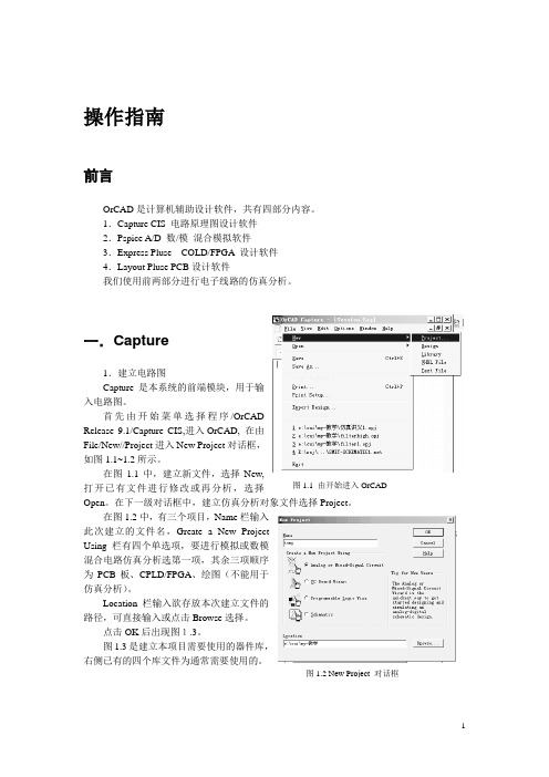
三.
Prob模块显示窗模拟示波器的显示效果,同时可对图形进行适当的分析。
在显示窗上增加图形。点击后出现下面对话框:
左边栏目选择要显示波形的节点处。右边栏目可选择计算公式。下边栏目列表达式。点击OK按键后,对应节点表达式的波形将显示在屏幕上。用这种办法可得到更多的显示信息。比如可用输入电压比输入电流得到输入阻抗。
噪声分析是计算电路各部分在各点频上的噪声等效为输入噪声源位置上的输入噪声。以此计算出等效输出噪声,结果以文件的形式输出。可在输出文件中查到。
Bias Point:
在分析偏置时,Pspice将电路中的电容开路电感短路,对各信号源取其直流电平值,用迭代法计算电路的直流偏置状态。
在Analysis type栏中选中bias Point,Options栏中选中Save Bias Point,Output file options栏选中Include detailed bias point information for nonlnear controlled sources and semiconductor,就可以进行偏置(直流工作点)分析了。Perform Sensitivity analysis用于直流灵敏度分析,Calculate small-signal DC gain用于计算直流传输特性分析。
傅立叶变换,进行时域分析后选此按键可进行傅立叶变换,结果以频谱显示在屏幕上。
文本标签,在屏幕上设置文本标签。
测试点坐标,测试任意点的坐标。
标注座标值。
*点击菜单栏的window/copy to clipboard可将屏幕显示的图形放入剪贴版,粘贴到word文档中。
orcad 电路仿真
OrCAD/PSpice9的电路仿真方法1、概 述1.1 PSpice 软件P S p i c e是一个电路通用分析程序,是E D A中的重要组成部分,它的主要任务是对电路进行模拟和仿真。
该软件的前身是S P I C E(S i m u l a t i o n P r o g r a m w i t h I n t e g r a t e d C i r c u i t E m p h a s i s),由美国加州大学伯克莱分校于1972年研制。
1975年推出正式实用化版本S P I C E2G,1988年被定为美国国家标准。
1984年M i c r o s i m公司推出了基于S P I C E的微机版本P S p i c e (P e r s o n a l-S P I C E),此后各种版本的S P I C E不断问世,功能也越来越强。
进入20世纪90年代,随着计算机软件的飞速发展,特别是W i n d o w s操作系统的广泛流行,P S p i c e又出现了可在W i n d o w s环境下运行的5.1、6.1、6.2、8.0等版本,也称为窗口版,采用图形输入方式,操作界面更加直观,分析功能更强,元器件参数库及宏模型库也更加丰富。
1998年1月,著名的E D A公司O r C A D公司与开发P S p i c e软件的M i c r o s i m公司实现了强强联合,于1998年11月推出了最新版本O r C A D/P S p i c e9。
为了迅速推广普及O r C A D/P S p i c e9软件,O r C A D公司提供了一张试用光盘O r C A D/P S p i c e 9D e m o, 它与商业版是完全一致的,不同之处只是在元器件上受到一定的限制,因此又被称为普及版。
本章将以普及版为例简要介绍O r C A D/P S p i c e9的功能及使用方法。
本书中所有的虚拟实验都是用O r C A D/P S p i c e9D e m o完成的,所引用的屏幕画面也都是出自于O r C A D/P S p i c e 9D e m o软件。
PT静态时序分析的三种模式
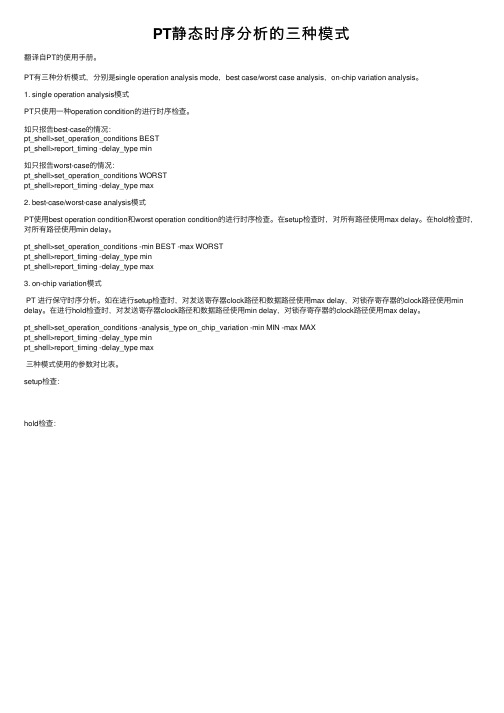
PT静态时序分析的三种模式翻译⾃PT的使⽤⼿册。
PT有三种分析模式,分别是single operation analysis mode,best case/worst case analysis,on-chip variation analysis。
1. single operation analysis模式PT只使⽤⼀种operation condition的进⾏时序检查。
如只报告best-case的情况:pt_shell>set_operation_conditions BESTpt_shell>report_timing -delay_type min如只报告worst-case的情况:pt_shell>set_operation_conditions WORSTpt_shell>report_timing -delay_type max2. best-case/worst-case analysis模式PT使⽤best operation condition和worst operation condition的进⾏时序检查。
在setup检查时,对所有路径使⽤max delay。
在hold检查时,对所有路径使⽤min delay。
pt_shell>set_operation_conditions -min BEST -max WORSTpt_shell>report_timing -delay_type minpt_shell>report_timing -delay_type max3. on-chip variation模式PT 进⾏保守时序分析。
如在进⾏setup检查时,对发送寄存器clock路径和数据路径使⽤max delay,对锁存寄存器的clock路径使⽤min delay。
在进⾏hold检查时,对发送寄存器clock路径和数据路径使⽤min delay,对锁存寄存器的clock路径使⽤max delay。
第八章综合与STA

flow
Inputs: gate level netlist, floor plan, timing constraint, lib setup file
Optimizing existing gate level netlist according to the placement
• Starting from the bottom of the hierarchy
and proceeding up through the levels of the hierarchy until the top-level design is compiled
Top
A
B
5 ns 25 ns
• Gate-Level optimization
Delay optimization Design rule fixing Area optimization
• Timing correction is most effective with
placement information
E.g., Physical synthesis
• It does not use wire load-models
The delay is calculated based on placement rather than fanout
• Benefits
Frontend designers can consider physical effects earlier in the design process
targeting and optimizing individual blocks
时序分析与时序约束

时序分析与时序约束(基于TimeQuest Timing Analyzer)一、基础篇:常用的约束(Assignment/Constraints)分类:时序约束、区域与位置约束和其他约束。
主要用途:1、时序约束:规范设计的时序行为,表达设计者期望满足的时序条件,指导综合和布局不同阶段的优化算法等。
简而言之就是规范和指导的作用。
倘若合适的话,它在综合、影射、布局布线的整个流程中都会起指导作用,综合器,布线器都会按照你的约束尽量去努力实现,并在静态时序分析报告中给出结果。
2、区域与位置约束:指定芯片I/O引脚位置以及指导实现工具在芯片中特定的物理区域进行布局布线。
3、其他约束:主要作用:1、提高设计的工作频率:通过附加时序约束可以控制逻辑的综合、映射、布局和布线,以减少逻辑和布线的延时。
其实,综合后的结果只是给出你的设计一个大概的速度范围,布线后的速度比综合后给出的结果要低,这是因为综合后只有器件的延时,而布线后除了器件的延时还要加上布线上的延时。
至于低多少就看设计者的约束能不能很好的指导布线器进行优化了。
2、获得正确的时序分析报告:在QuartusII 中,内嵌的是静态时序分析工具(STA, Static Timing Analysis),他的作用就是设计进行评估,只有在正确的输入时序约束的情况下,才能得到可靠的报告。
同时也是做FPGA设计时是必须的一个步骤,事实上大家一般都已经做了这一步,我们在FPGA加约束、综合、布局布线后,会生成时序分析报告,设计人员会检查时序报告、根据工具的提示找出不满足setup/hold time的路径,以及不符合约束的路径,这个过程就是STA。
此外,STA是相对于动态时序仿真而言的,它通过对每个时序路径的延时分析,计算出最高的设计频率(fmax),发现时序违规(Timing Violation)。
注意:静态时序分析仅仅聚焦于设计时序性能的分析,而不会涉及逻辑性能。
在STA中主要分析的路径有:时钟路径,异步路径,数据路径。
case analysis范文
case analysis范文Case Analysis: An In-depth Examination of a Specific CaseIntroduction:Case analysis is a method used to study and understand a specific case thoroughly. It involves a detailed examination of the case, identification of key issues, analysis of possible solutions, and recommendations for future actions. In this article, we will discuss the importance of case analysis and its relevance in various fields.Body:1. Importance of Case Analysis:Case analysis is essential for several reasons. Firstly, it allows researchers to gain a deep understanding of the case under study. By analyzing the details, context, and intricacies of a case, researchers can identify patterns, causes, and effects. This comprehensive understanding helps in making informed decisions and formulating effective strategies.2. Process of Case Analysis:The process of case analysis typically involves several steps. These include:a) Identifying the Problem: The first step is to identify the problem or issue that needs to be addressed. This requires a clear understanding of the case and its context.b) Gathering Relevant Information: Once the problem is identified, the next step is to gather all the relevant information related to the case. This may include data, documents, interviews, or other sources.c) Analyzing the Information: After gathering the information, it is important to analyze it critically. This involves identifying patterns, trends, and relationships among the data points.d) Developing Solutions: Based on the analysis, potential solutions or strategies can be developed. These solutions should address the root causes of the problem and be feasible to implement.e) Evaluating Alternatives: It is important to evaluate the potential solutions and compare them based on their feasibility, effectiveness, and potential impact. This helps in selecting the most suitable solution.f) Making Recommendations: Finally, based on the evaluation,recommendations can be made for future actions. These recommendations should be practical, actionable, and aligned with the goals of the case.3. Applications of Case Analysis:Case analysis is widely used in various fields, including business, law, medicine, and social sciences. Some specific applications include:a) Business Strategy: Case analysis is often used in the business world to analyze market trends, competitive landscapes, and customer behavior. It helps in formulating effective strategies and making informed business decisions.b) Legal Cases: In the field of law, case analysis is crucial for understanding legal precedents, interpreting legislation, and building strong arguments. It allows lawyers to analyze past cases and apply relevant legal principles to their case.c) Medical Research: Case analysis plays a significant role in medical research. It helps in understanding diseases, identifying risk factors, and developing treatment protocols. Case analysis also helps in identifying potential adverse events and improving patient outcomes.d) Social Sciences: In social sciences, case analysis is used to study human behavior, societal issues, and cultural phenomena. Researchers analyze individual cases to draw broader conclusions and understand social patterns.Conclusion:Case analysis is a valuable method for gaining a deep understanding of a specific case. By following a systematic process, researchers can identify key issues, analyze information, and develop effective solutions. This method finds applications in various fields and contributes to informed decision-making and problem-solving. Mastering the art of case analysis can be beneficial for professionals in diverse industries.。
工艺角 corner

工艺角(Process Corner)与双极晶体管不同,在不同的晶片之间以及在不同的批次之间,MOSFETs参数变化很大。
为了在一定程度上减轻电路设计任务的困难,工艺工程师们要保证器件的性能在某个范围内,大体上,他们以报废超出这个性能范围的芯片的措施来严格控制预期的参数变化。
detail通常提供给设计师的性能范围只适用于数字电路并以“工艺角”(Process Corner)的形式给出。
如图,其思想是:把NMOS和PMOS晶体管的速度波动范围限制在由四个角所确定的矩形内。
这四个角分别是:快NFET和快PFET,慢NFET 和慢PFET,快NFET和慢PFET,慢NFET和快PFET。
例如,具有较薄的栅氧、较低阈值电压的晶体管,就落在快角附近。
从晶片中提取与每一个角相对应的器件模型时,片上NMOS和PMOS的测试结构显示出不同的门延时,而这些角的实际选取是为了得到可接受的成品率。
各种工艺角和极限温度条件下对电路进行仿真是决定成品率的基础。
所以我们所说的ss、tt、ff分别指的是左下角的corner,中心、右上角的corner。
工艺极限 (Process Corner)如果采用5-corner model会有TT,FF,SS,FS,SF 5个corners。
如TT指NFET-Typical corner & PFET-Typical corner。
其中, Typical指晶体管驱动电流是一个平均值,FAST 指驱动电流是其最大值,而SLOW指驱动电流是其最小值(此电流为Ids电流)这是从测量角度解释,也有理解为载流子迁移率(Carrier mobility)的快慢. 载流子迁移率是指在载流子在单位电场作用下的平均漂移速度。
至于造成迁移率快慢的因素还需要进一步查找资料。
单一器件所测的结果是呈正态分布的,均值在TT,最小最大限制值为SS与FF。
从星空图看NFET,PFET所测结果,这5种覆盖大约+-3 sigma即约99.73% 的范围。
华中科技大学电子线路测试实验01-PSPICE仿真130701

实验一
PSpice软件仿真练习(一)
• 电子线路CAD概述 • OrCAD/PSpice仿真软件操作介绍 • 本次实验内容及要求
一、电子线路CAD概述
1、什么是“电子电路计算机仿真”
就是用计算机来帮助人们分析或者设计电子 电路。它是CAD和EDA技术的重要组成部分。
电子电路设计就是根据给定的功能和特 性指标要求,通过各种方式,确定电路采用 的拓扑结构及各个元件的参数值。
• 参数扫描 包括温度特性分析(Temperature Analysis)
参数扫描分析(Parametric Analysis)。
(5)统计分析 包括蒙托卡诺分析(MC:Monte
最坏情况分析(WC:Worst Case)。
Carlo)、
(6)逻辑模拟 包括逻辑模拟(Digital Simulation)、数/模混合
(2)比例因子只能用英文字母,如10-6用U或u表示, 而国标规定10-6用希腊字母m表示。故如 电容容量 C=1×10⁻⁶F,应写成C=1u(或1U)
实验电路分析具体操作流程
绘制电路图
放元件 放电源
设置分析类型
连线
存盘 电气规则检查
编辑元件和 电源参数
生成网表
分析(调用Pspice) Probe观察波形
(2)PSpice 模块
PSpice 模块是通用电路模拟软件。除可对模 拟电路、数字电路和数/模混合电路进行模 拟外,还具有优化设计的功能。该软件中的 Probe模块,不但可以在模拟结束后显示结果 信号波形,而且可以对波形进行各种运算处 理,包括提取电路特性参数,分析电路特性 参数与元器件参数的关系。
case analysis method
case analysis methodCase Analysis MethodCase analysis method is a common approach used in business and management education to teach students how to solve real-world problems. This method involves analyzing a specific case study to identify the key issues, evaluate alternative solutions, and make recommendations for action. In this article, we will discuss the steps involved in the case analysis method and its benefits.Step 1: Understanding the CaseThe first step in the case analysis method is to read and understand the case study. This involves identifying the key issues, the industry, and the company's background. It is important to have a clear understanding of the case before moving on to the next step.Step 2: Analyzing the CaseThe second step is to analyze the case study. This involves identifying the problems faced by the company, evaluating the alternatives, and selecting the best course of action. Theanalysis should be based on facts and data, and should consider the impact of each alternative on the company's future.Step 3: Developing RecommendationsThe third step is to develop recommendations for action. This involves outlining a specific course of action that the company should take to address the problems identified in the case study. The recommendations should be based on the analysis and should be feasible, actionable, and effective.Benefits of Case Analysis MethodThe case analysis method offers several benefits to students and business professionals. Firstly, it provides an opportunity to apply theoretical concepts to real-world problems. This helps students develop critical thinking and problem-solving skills that are essential in the business world. Secondly, it enables students to work collaboratively and develop effective communication and teamwork skills. Finally, the case analysis method provides a deeper understanding of the complexities of the business world and the challenges faced by organizations.ConclusionThe case analysis method is a valuable tool for teaching students how to solve real-world problems in the business world. It involves analyzing a specific case study to identify the key issues, evaluate alternative solutions, and make recommendations for action. By using this method, students can develop critical thinking, problem-solving, communication, and teamwork skills that are essential in the business world.。
STA和门级仿真结合的新方法

前言静态时序分析以它运行速度很快、占用内存较少,可以对芯片设计进行全面的时序功能检查,并利用时序分析的结果来优化设计等优点,很快地被用到数字集成电路设计的验证中。
然而门级仿真也由于它不可取代的地位在ASIC设计中仍有一席之地。
结合在TDS-CDMA数字基带处理芯片设计中的经验,我们可以得出这样的结论:静态时序分析和门级时序仿真是从不同的侧重点来分析电路以保证电路的时序正确,它们是相辅相成的。
现在,实验中的TDS-CDMA数字基带处理芯片已经成功流片。
本文的创新点在于,在实践中寻找到一种STA和门级仿真结合的新方法。
在保证流片成功率的基础上最大程度的节省芯片验证的时间。
关键词:静态时序分析门级时序仿真芯片随着深亚微米技术的发展,数字电路的规模已经发展到上百万门甚至上千万门。
工艺也从几十μm提高到65nm甚至45nm。
这样的电路规模做验证的时间在整个芯片的开发周期所占的比例会越来越重。
通常,在做验证的时候,我们都会采用动态验证的方法。
现在,用静态验证方法(STA Static Timing Analysis),不仅能够完成验证的工作,而且还能大大节省验证所需要的时间。
静态时序分析简称它提供了一种针对大规模门级电路进行时序验证的有效方法。
静态时序分析是相对于动态时序分析而言的。
动态时序分析时不可能产生完备的测试向量,覆盖门级网表中的每一条路径。
因此在动态时序分析中,无法暴露一些路径上可能存在的时序问题;而静态时序分析,可以方便地显示出全部路径的时序关系,因此逐步成为集成电路设计签字认可的标准。
静态时序分析工作原理本文以Synopsys公司的Prime Time SI作为时序分析的工具,介绍静态时序分析的工作原理。
Prime Time把整个设计电路打散成从主要的输入端口到电路触发器、从触发器到触发器、从触发器到主要输出端口、从主要的输出端口到主要的输出端口、四种类型的时序路径,分析不同路径的时序信息,得到建立时间(setup time)和保持时间(hold time)的计算结果。
PrimeTime

--Set and Remove a False Path Exception
• 建立和删除伪路径例外 1.申明一个伪路径from pin g1/CP to g13/D: pt_shell> set_false_path -from g1/CP -to g13/D 2.指出设计的时序例外: pt_shell> report_exceptions ... From To Setup Hold Ignored -------------------------------------------------g1/CP g13/D FALSE FALSE ... 3.删除例外: pt_shell> reset_path -from g1/CP -to g13/D pt_shell> report_exceptions //查看报告
pt_shell> all_fanout -from g1/CP -endpoints_only 3.重置伪路径 pt_shell> reset_path -from g1/CP(伪路径的设置与重置的方式要对应,否则无法重 置,如此处若用 pt_shell> reset_path -from g1/CP -to g13/D 重置,则无效,因为建 立为路径是用的是-from) 4.通过组合逻辑设置更特殊的伪路径: pt_shell> set_false_path -setup \ -from g1/CP -through g9/Z -to g13/D 5.重置时序例外 pt_shell> reset_path -from g1/CP pt_shell> report_exceptions 例外的设置命令可以是reset_path命令的子集,但reset_path命令不可以是例外设置 命令的子集
Analysis of Delay Test Effectiveness with a Multiple-Clock Scheme
Analysis of Delay Test Effectiveness with a Multiple-Clock Scheme Jing-Jia Liou,Li-C.Wang,and Kwang-Ting ChengDepartment of ECE,UC-Santa Barbarajjliou,licwang,timcheng@Jennifer Dworak,and M.Ray MercerDepartment of EE,Texas A&M Universityjdworak,mercer@Rohit Kapur,and Thomas W.WilliamsSynopsys Inc.rkapur,tww@AbstractIn conventional delay testing,two types of tests,transition tests and path delay tests,are often considered.The test clock fre-quency is usually set to a single pre-determined parameter equal to the system clock.This paper discusses the poten-tial of enhancing test effectiveness by using multiple test sets with multiple clock frequencies.The two intuitions motivating our analysis are1)multiple test sets can deliver higher test quality than a single test set,and2)for a given set of AC de-lay patterns,a carefully-selected,tighter clock would result in higher effectiveness to screen out potentially defective chips. Hence,by using multiple test sets,the overall quality of AC de-lay test can be enhanced,and by using multiple-clock schemes the cost of adding the additional pattern sets can be minimized. In this paper,we analyze the feasibility of this new delay test methodology with respect to different combinations of pattern sets and to different circuit characteristics.We discuss the pros and cons of multiple-clock schemes through analysis and ex-periments using a statistical delay evaluation and delay defect-injected framework.1IntroductionIn traditional AC delay test and validation,two sets of patterns are often applied.They are the transition fault patterns and the critical path test patterns.Conventional wisdom usually dif-ferentiates the two by the sizes of delay defects they intend to capture.On one hand,transition fault patterns are considered to be more effective for large-size delay defects which can hap-pen randomly at any site of a circuit.On the other hand,criti-cal path test patterns aim to detect small-size delay defects on a selected set of long timing paths.It is then hoped that the com-bination of these two orthogonal strategies can capture most of the delay defects and ensure the circuit performance.By definition,transition fault test generation does not rely on a timing analysis tool.For a given site,delay faults can be observed through any of the sensitizable paths.Hence,the delay defect sizes captured by transition fault tests are not guaranteed.The longer the timing of the paths used to de-tect the faults,the smaller the sizes of defects they can cap-ture.Without explicitly targeting specific paths,employing multiple-detections becomes an alternative for enhancing the quality of transition test set effectiveness[5].The quality of path delay tests,on the other hand,depends on the use of a timing analysis tool to accurately estimate the timing lengths of the paths.Assuming an ideal timing analy-sis tool is in hand,a set of critical paths can be derived.AC patterns are then produced to specifically test these paths.Test generation for target paths is not a trivial task,especially for paths whose robust detection is not possible[10].Hence,an ideal critical path set does not imply that an ideal test pattern set can be generated.In traditional timing analysis,delay models are often dis-crete and based upon nominal or worst-case timing assump-tions[3,4,6,7].Such models become increasingly inadequate because,in the deep sub-micron domain,factors affecting de-lay characteristics(such as process variations,manufacturing defects,and noise)can often be continuous in nature[1,2,8,9]. These continuous factors can be better captured and simulated using statistical models and methods[11,12,13].Hence,de-lays should be modeled with random variables instead of with discrete values.This adds tremendous complexity to path delay fault testing.With statistical delay models in mind,the focus of this paper does not lie in maximizing the test effectiveness for transition fault patterns nor in selecting the true longest paths for path de-lay testing.Instead,we explore another alternative to improve delay test quality–by applying the test patterns in phases with different clock frequencies.We assume that a set of test pat-terns is already given.Then,the question is how to apply an additional test set(s)to further enhance the test quality with minimal additional cost.It is important to note that,with the methodology introducedin this paper,applying the same patterns at different clock fre-quencies will not enhance the test quality of a given pattern set(This point will be further illustrated in Section3).Hence, to improve test quality,our strategy is the following:Given a set of patterns,a second set of patterns is added.Test qual-ity is improved by combining the two pattern sets.However, the application of tests is divided into two phases:the screen-ing phase and the confirmation phase.In the screening phase, the goal is to use thefirst set of patterns with a tighter clock scheme to screen out potentially defective chips.Then,in the confirmation phase,both sets of patterns are applied with the normal clock to confirm which chips are actually bad.The key of this strategy is the selection of the clock scheme in the screening phase in order to minimize the cost during the con-firmation phase.The goal is to achieve a test quality similar to that obtained by applying both test sets in the traditional way and yet,with a cost closer to that of applying only thefirst test set alone.Our earlier work[14]proposed using the2-phase test scheme based upon double-transition test set,and concluded that during the screening phase,using only one tighter clock might not be enough.In this paper,we discuss the potential of applying a multiple-clock scheme(where more than one tighter clocks are used during the screening phase)with different com-binations of test sets and with designs of different timing char-acteristics.We explore the advantages and limitations of using the multiple-clock scheme for enhancing delay test effective-ness.Our conclusion is that without an ideal timing analysis tool and a perfect path-delay ATPG tool,combining multiple-clock scheme and multiple-detection transition test sets will be a feasible solution in practice for improving delay test quality, especially for timing-optimized high-performance designs.This paper is organized as the following.Section2de-scribes the background and motivation for our work.Section3 presents the methodology of using a multiple-clock scheme for test quality improvements and discusses related issues.Sec-tion4illustrates our experimental setting and presents experi-mental results based on an ISCAS benchmark circuit.In sec-tion5,we analyze the feasibility of the proposed clock scheme with respect to different combinations of test sets and to differ-ent circuit characteristics.Section6concludes the paper.2Background and Motivation Several publications[15,16,17,18]have tried to use variable or multiple clock schemes to improve the detection of delay de-fects.Unfortunately,there is one serious drawback with these schemes:the false negative outcomes.It is possible that most chips considered“bad”by these schemes are actually function-ally correct and have correct timing.This is because most delay defects that increase the delays of some paths may not actually be located on the critical timing paths.This problem will re-sult in an unnecessary increase in the number of parts deemed defective and a decrease of the total yield(yield loss).There-fore,for practical use of a multiple-clock scheme,thefirst key concern is to avoid yield loss.In conventional AC delay test,the transition fault model and path delay model represent two orthogonal testing strategies.Assume that a set of100%transition patterns sensitizes thepaths P tran l1l n and a set of path delay patterns sensi-tizes P path p1p k.Let M be an ideal timing model such that given a path p,M p denotes the delay of the path.And let C be the clock.Then,by covering P tran,all the single-sited de-fects with sizes larger thanθtran C min M l1M l n are expected to be captured.Similarly,all the defects with sizes larger thanθpath C min M p1M p k will be captured if the defects fall on a path in P path.If M is a statistical model, we note that bothθtran andθpath are random variables,not sin-gle values.In general,we should haveθtranθpath.In transition fault testing,P tran does not always contain the longest path passing through a site.To improve transition test quality,it is intuitive to improve the quality of P tran by sensitiz-ing the path with longest propagation time l maxipassing through each site i.However,the cost of doing so will be similar to that of path delay testing,and the quality will once again be highly dependent on the timing model M.The quality of P path depends on the accuracy of M.In thedeep sub-micron domain,the accuracy of M is not easy to de-fine,and traditional timing analysis will often fail to provide a good delay prediction.The topological coverage of P path may also affect the quality.The topological coverage of P path con-cerns the site coverage.If P path covers every site,then any single-sited delay defect,in theory,will be captured.In this case,those defects that are not captured will not affect the cir-cuit performance.However,normally,it is not expected that P path covers every site.(In that case,P path could replace tran-To illustrate the above analysis,Figure1demonstrates com-parison results between transition patterns and path delay pat-terns.These results were obtained using the statistical timing analysis framework developed before[13].For a particular de-fect size,1000randomly-located defects are injected onto the circuit(this is ISCAS benchmark s5378).Then,we collect the statistics of unique defect detection.In thefigure,two pattern combinations are analyzed:single-detection transition patterns(tfp1)vs.path delay fault patterns (pdf),and double-detection transition patterns(tfp2)vs.thesame path delay patterns.Here,we are interested in the uniquedetection within each combination.For example,in the case of defect size15units,(if they are detected)there is no defect uniquely detected by the single-detection transition patterns. All detected defects are captured through the path delay pat-terns.For the double-detection transition patterns,still there is no unique detection.However,the unique detection from the path delay patterns drops due to a higher overlap of the detec-tion between the double-detection patterns and the path delay patterns.In general,several things can be observed from thefigure: Transition fault patterns are better for large-size defects (contribute more unique detections when the defect sizes are large).Path delay patterns are better for small-size defects,and since the patterns do not cover all sites in the circuit,for large defects its value can saturate.(Once a defect fallsbeyond the topological coverage,it has no chance of be-ing detected.)Double-detection transition patterns are better thansingle-detection transition patterns.In addition,because of the higher overlap of detection between the double-detection patterns and the path delay patterns,the uniquedetection of the path delay patterns decreases.The benefit of using double-detection transition patterns is clearly shown in thefigure.However,the major problem ofusing double-detection patterns is its high test application cost. Normally,for state-of-the-art high-performance designs such as microprocessors,applying single detection patterns wouldhave already consumed a majority of the test application re-sources(tester memory,time,etc.).It is hence very difficult to adopt another complete transition pattern set in practice.The strength of a transition pattern set lies in its complete topological coverage of the circuit.Its weakness is the ability to detect small-size defects.Multiple-detection can enhancethat ability with a relatively high cost.Is there any other alter-native so that we can keep the benefit of going for a multiple-detection strategy but without the high cost associated with it?Our answer is based upon alternating the test clock C.In-stead offixing the test clock to be the same as the system clock,we can carefully devise a test clock scheme which con-sists of multiple clocks.For example,when pattern set1is applied,instead of using C we may use a different clock Cδ. By doing so,any single-sited defect with a size greater thanθalt Cδmin M l11M l1n will be screened out.Be-causeθaltθtran,smaller defects that were not detectable be-fore can be captured now.Hence,we have enhanced the ability to screen out“defective”chips.Notice that by applying tests with a tighter clock,a good chip passing the new clock Cδwould still be classified as a good chip if the same set of pat-terns is applied with the original clock C.However,the reverse is not true:a failing chip may still pass the same test set with C.In this case,we may have a yield loss.In the next section,we will discuss how a multiple-clock scheme should be devised to avoid the problem of yield loss and at the same time improve quality with minimal cost.Then,throughout the rest of the paper,we will focus our discussion on the following two issues:What combination(s)of multiple test sets will be mosteffective to be applied with a multiple-clock scheme?What circuit characteristics are most suitable for using amultiple-clock scheme?We will analyze these issues based upon transition fault testand path delay fault test strategies,using both un-optimizedand optimized circuits,and under a statistical delay evaluation and defect-injected simulation framework.3Multiple-Clock SchemeFor simplicity of discussion,we assume two100%sets of tran-sition fault patterns A and B are given.Let A cover pathsT1l11l1n,and let B cover paths T2l21l2n for sites1n,respectively.Our goal is tofind a clock scheme such that the cost is minimized relative to the cost of applying onlyone set,and the quality is maximized relative to the quality ofapplying both sets.Our methodology employs a2-phase test application pro-cess:a screening phase and a confirmation phase.During thescreening phase,tighter clocks are used with the application of test set A to quickly screen out the potentially bad chips.Then, during the confirmation phase,the normal clock is used with the test set A B to avoid yield loss.We note that,to avoid yield loss,it is necessary to applyboth A and B with the normal clock during the confirmationphase in order tofilter in good chips that were considered to be defective during the screening phase.Therefore,with this methodology,it is important to note that alternating the clock by itself will not improve the quality beyond that obtained by applying both A and B with the normal clock.Hence,A B combined with the normal clock will represent an upper bound (in terms of test quality)for using a multiple-clock scheme.In other words,the total number of defective chips captured in the new scheme cannot be greater than that captured by the original A B combined with the normal clock.Assume that the tighter clock is Cδ.The following dis-cusses the concepts of defect miss and yield loss in more detail. Defect Miss A chip passing the screening phase may be defec-tive and still could be captured if B were applied with the normal clock.However,it is guaranteed that the passed chip will still pass if A is applied with the normal clock.Based upon these points,it is possible that some defectsare missed under the new test application scheme butcould be captured by the original test method where A B is applied with the normal clock.How likely is this to happen?Consider a given site i.A true defect(which can affect circuit performance)on iwill be missed if its size d falls into the range C M l2iCδM l1i.This implies M l1iδC d M l2i(see Figure2).With a reasonably largeδ,it is unlikelythat M l2i M l1iδ.Even when this is happening, the chance of a defect occurrence with a size that fallsexactly into the range is small.Hence,the problem of a defect miss is not a serious concern.One may think that to avoid defect miss,we should set δas large as possible.However,a large δ(a tighter clock)will increase the potential yield loss as explained below.1+1++Figure 2:Illustration of Defect Miss and Yield LossPotential Yield Loss Yield loss is defined as the percentage ofchips that are considered to be defective by the tests but are actually good chips.In our scheme,since we have al-ready used A B and the normal clock in the confirmation phase to prevent yield loss from happening,the key here is how likely will potential yield loss happen at the end of screening phase?In other words,if many chips are deter-mined to be bad in the screening phase,then these chips will be tested by A B again.Hence,the higher such a potential yield loss is,the higher the cost of the proposed testing scheme will be.Similarly to the defect miss situation,a defect at site i will result in potential yield loss (at the end of the screen-ing phase)if its size d falls into the range C δM l 1i C max M l 1i M l 2i (see Figure 2).This implies thatmax M l 1i M l 2i C d δM l 1i .Hence,to min-imize potential yield loss during the screening phase (and hence the overall test application cost),δshould be as small as possible.From the figure,we note that for a fixed δand a fixed site i ,a defect miss and potential yield loss cannot happen at the same time.The Selection of δThe above analysis suggests two contradictory objectives for the selection of δ.On one hand,δshould be large to avoid a defect miss.On the other hand,δshould be small to mini-mize the test cost resulting from the effort of avoiding yield loss during the confirmation phase.By combining the two ob-jectives,it seems that the most logical solution is to set a differ-ent δi M l 1i M l 2i for each site i .This is obviously not an easy thing to accomplish because we may need to supply so many different test clocks during testing,and even though that is possible with a high cost,ensuring that the timing model M accurately reflects the reality is also difficult.3.1Clock Scheme in the Screening PhaseThe compromise solution is to employ k multiple clocks in the screening phase,where k is a small number.Our strategy is to first partition a given test set (A )in the screening phase into k subsets.Then,for each subset,a different clock is determined.Test Set Partitioning Given a set of patterns,we use thestatistical timing analysis tool M [13]to characterize the delay distribution of the longest sensitizable path passing through each site (again denote these results asM l 11M l 1n ).Next we compute the mean value in each distribution (assume that the order is m l 11m l 1n).Then,the partition is based upon the difference D m l 1n m l 11.The first partition is to divide 0D into two ranges D 10εD and D 2εD D where εdenotes the ratio of partition and 0ε1(normally,05εbecause short paths are less important than the long paths).All paths whose mean timing values fall into the first range will be grouped into the first set S 1.The rest will be grouped into the second set S 2.Then,the same idea can be applied recursively to partition S 2fur-ther,and so on (see Figure 3).It is interesting to note that in our experiments,we discovered that the best results are often obtained by setting:ε11provide that coverage.The key reason is that a tighter clock will not help to capture a defect if the defect falls beyond the topological coverage of a pattern set.Withouta complete topological coverage,the number of defectmisses could be high.The multiple-clock scheme alone will not help to improve test quality.The improvement of quality actually comes from the addition of the second pattern set.The usage of the multiple-clock scheme is to greatly reduce the cost associated with the inclusion of the second pattern set.In essence,the goal of the screening phase is to quickly identify potentially defective chips.Then,in the confir-mation phase,a higher quality test set is applied to double check each potentially bad chip more carefully.The cost saving relies on the fact that the majority of the chips are good ones and hence,only a few chips would go into the confirmation phase.3.3Cost EvaluationGiven the two pattern sets,A and B,intuitively we may define the cost as AρA B whereρrepresents the probability of a chip classified as potentially defective during the screening phase.As discussed before,this probabilityρdepends on the clock(s)selected during the screening phase.In the next sec-tion,we will present ourflow to evaluateρunder the statisti-cal timing analysis framework.However,the true cost is not entirely reflected in the simple equation AρA B.This is because the calculation of cost should also take defect size distribution into account.Without loss of generality,we as-sume defect distribution is a discrete functionΓ.Then,for each defect size s,Γs gives the conditional probability that if a defect does occur,its size is s.Then the true cost should be re-formulated as:Cost A∑sΓsρs A B(1) where s is the defect size andρs is the probability of a chip being classified as a defective chip during the screening phase due to a defect with size s.In essence,equation(1)calculates the cost by averaging across the defect distribution curve.If the defect distribution is uniform,then the equation will be reduced to“AρA B,”whereρ∑sρs.3.4Cost Vs.Quality GainWe note that in the proposed multiple-clock methodology,the quality of the overall test scheme is determined by the quality of“A B.”The cost depends onρand the size of“A B.”Suppose the size of B is relatively small with respect to A,and the quality of B is very high.Then,using the multiple-clock method will have little gain in this case because A A B. In other words,using the multiple-clock scheme will not be better than just applying A B together with a normal clock.As mentioned before,A has to be a transition fault pattern set to ensure a complete topological coverage.For B,if a small-size high-quality path delay pattern set is available,then the multiple-clock scheme will be of little usefulness.However,we emphasize that the quality of a path delay pattern set de-pends on the timing tool and the test generation tool,whichboth are far from being perfect in reality.Moreover,the sizeof the path delay pattern set needed to achieve a desired highquality also depends on the circuit’s timing characteristics as well.Hence,in section5we will discuss how the circuit’s tim-ing characteristics may affect the effectiveness of the proposedmultiple-clock scheme.3.5Cost ReductionThe cost can be further reduced if we allow an extremely smallyield loss tolerance level.For example,we can select an upperbound t to restrict the target defect size during the confirmation phase such that for any large-size defect s,s t,andΓsεwhereεis a very small number such as104.Then,all shortpaths whose timing lengths less than C t(with high proba-bilities)in A can be removed during the confirmation phase. The intuition behind this is that these short paths will be of lit-tle help in deciding whether a potential defective chip after the screening phase is actually a good chip or not.Accordingly, we can remove all patterns that cover only those removed short paths.In the next section,we will demonstrate that ifΓis an exponential distribution,a large number of paths in A can be removed in the confirmation phase with very little increase(al-most zero)of the yield loss probability.As a result,the cost of applying our proposed test scheme can be dramatically re-duced,and the quality can be maintained.4Experiments4.1Evaluation FrameworkCoverageanalysisofSonthegivencircuitinstanceFigure4:Flow Chart for Statistical Evaluation of S We implemented a statistical delay evaluation framework to estimate the defect coverage based on simulation of random defect injection.Figure4illustrates the complete procedure of our evaluation scheme for a particular clock and pattern set. Note that the pattern set is characterized using the set of paths S sensitized by the patterns.In each Monte Carlo sampling run,first a circuit instance with cell/interconnect delays is gener-ated according to the delay distributions characterized through Monte Carlo SPICE.This instance will then be evaluated by“statistical analysis of S”.The “statistical analysis of S”is used to check if there is any path in S (on the given instance)longer than the testing clock C .If there is,then this instance is said to be faulty and covered by S (Captured ).At the end,our scheme will calculate the capture probability for S .For the multiple-clock scheme,the evaluation process is similar.Those circuit instances classified as Captured during the screening phase will further be tested in the confirmation phase.Then,at the end,a Captured probability number will be produced.This statistical delay evaluation framework requires pre-characterization of cells,i.e.,building libraries of pin-pin cell delays and output transition times (as random variables).In our experiments,we utilize a Monte-Carlo-based SPICE (ELDO)[19]to extract the statistical delays of cells for a 0.25µm,2.5V CMOS technology.The input transition time and output loading of the cells are used as indices for build-ing/accessing these libraries.4.2Initial ResultsIn the initial experiments,three test sets are considered:two single transition fault test sets,and a path delay fault set.For the path delay fault set,we will select statistically long paths [13]which are functionally sensitizable [10].Without a perfect path delay test generator,we assume one test for each selected path.In a sense,this represents the optimal situation (there ex-ists a test for every selected path and an ATPG tool can always produce the test).In the following,we explain results from circuit s5378.Fig-ures 5and 6present test quality levels that resulted from the multiple-clock scheme.In the figures,we demonstrate,for each method,its ability to capture defects of various sizes.We note that since our objective here is to compare the rela-tive strength among different methods,the absolute values oftern Sets Using Different Clock SchemesIn Figure 5we combine th two transition fault pattern sets.In Figure 6we combine the first transition fault pattern set with the path delayset where the (statistically)longest 40paths are selected.For the multiple-clock scheme in the screening phase,Path Delay Pattern Sets Using Different Clock Schemes the partition number k is set to 3,and the ratio of partition εis set to 114.3Cost ComparisonTF2TF1-20.460.72cost(%) 1.006 2.006 reduced cost t150 1.006 2.0061.000 1.027reduced cost t50 1.006 2.006 TF1:1st transition set with normal clockTF2:2nd transition set with normal clock(TF1-2):two sets combined with the multiple clock schemeTF1-2:two sets combined with normal clock(TF1/PDF)capture prob.0.82cost(%) 1.1420.033 1.0330.033 1.0330.033 1.033PDF:path delay fault set with normal clock(TF1/PDF):1st transition set path delay set with multiple clocksTF1/PDF:1st transition set path delay set with normal clock Table1:Test cost and capture probability comparison for dif-ferent delay fault sets and clock schemes for s5378.Table1demonstrates the capture probabilities and cost com-parison results for different testing schemes.The costs are cal-culated by the formula in section3.3and based on the assump-tion of a defect size distribution:λeλs where s is the defect size andλis a constant(we useλ01in the experiments). This exponential distribution for defect size(given that defects occur)has been studied in many publications[20,21]and is a practical assumption to be used.Note that it is also possible to adopt other distributions.However,using other distributions in general does not invalidate the trends observed in our analysis.In the table,we also consider the cost reduction approach discussed in section3.5.The t value in each case is shown in the table.Note that by assuming the given defect distribu-tion,the probability of yield loss is0.000676for the worst case shown in the table(where t50units).We note that by def-inition,the yield loss is zero without involving the cost reduc-tion.Hence,this demonstrates that the proposed cost reduction scheme has a very small(but non-zero)probability of incurring a yield loss.We note that the costs presented in the table are normalized with respect to the cost of TF1.Data in this table confirm our earlier observations:The quality that resulted from the multiple-clock scheme “(TF1-2)”is close to the quality that resulted from two sets combined“TF1-2.”When using two transition test sets,the cost without re-duction can be high(127.4%).However,with cost reduc-tion,the cost can be reduced to almost the same as TF1.Notice that in case of cost reduction(meaningful only for (TF1-2)),by linearly decreasing the t value,the cost can drop in terms of an order of magnitude.In this analysis,a high-quality small-size path delay test set could be obtained.Hence,notice that in this case,themultiple-clock scheme does not provide much benefit,as expected.In reality,obtaining a high-quality small-size path delay set is very hard.Hence,multiple transition test sets combined with the multiple-clock scheme provides a much easier and practi-cal alternative to enhance test quality.However,in the table, we see that the quality of combining two transition test sets re-mains far from that achievable by an ideal path delay test set. Results from this table motivate us to further the study of the effectiveness of the multiple-clock scheme.The key question now is:Under what condition can multiple transition test sets combined with the multiple-clock scheme approach the cost and effectiveness of a high-quality path delay test set?Our intuition is that the effectiveness of using the multiple-clock scheme depends upon the circuit’s timing characteristics.5In-Depth AnalysisIn this section,we investigate how the circuit’s timing char-acteristics may affect the effectiveness of the multiple-clock scheme.The goal is to identify the most suitable circuit styles to be applied with the proposed scheme.For example,a highly timing-optimized circuit with a shallow logic depth may be-have quite differently under the proposed scheme from a cir-cuit that has not been optimized for timing.To demonstrate the difference,two additional experiments were devised.Thefirst experiment demonstrates the effect of the timing optimization process on the effectiveness of using the multiple-clock scheme.Given the benchmark circuit s5378,we measure the quality results based upon different optimized versions of the design.In the second experiment,a highly optimized in-dustrial design is used to emphasize the timing optimization effect.5.1The Impact of Timing Optimization We generate three different versions of circuit s5378by apply-ing different timing optimization constraints in Synopsys De-sign Compiler[22].These three versions are denoted as“v1,”“v2,”and“v3,”where v3is most optimized,and v1is the orig-inal version without timing optimization.Our statistical timing analysis tool is used to characterize the path delay profiles for the three circuits.These profiles are shown in Figure8.Note that only functionally sensitizable paths are counted in the profiles.In the optimization process, we try to improve not only the maximum delays of the circuit but also the span of the delay spectrum.Both parameters are smaller in each succeeding version(v1v2v3).Again,we consider two transition fault test sets combined with the multiple-clock scheme.In addition,we produce three more sets,PDF10,PDF50,PDF100which correspond to the(statistically)longest10,50,and100path sets,respec-tively.These selected paths are functionally sensitizable,and we again assume an ideal test generator is available to produce one test for each path.For the three versions of the circuit,the system clocks should be different as well to ensure a fair comparison.This is because v3can operate at a higher speed than v1.If the same。
安捷伦示波器使用方法

安捷伦⽰波器使⽤⽅法Jitter Analysis Techniques Using an Agilent Infiniium OscilloscopeProduct NoteIntroductionWith higher-speed clocking and data transmission schemes in the computer and communications industries, timing margins are becoming increasingly tight.Sophisticated techniques are required to ensure that timing margins are being met and to find the source of problems if they are not.This product note discussesvarious techniques for measuring jitter and points out theiradvantages and disadvantages. It describes how to set up an Agilent Infiniium oscilloscope to make effective jitter measure-ments and the accuracy of these measurements. Some of themeasurement techniques are only available on Agilent 54845A/B and 54846A/B oscilloscopes with version A.04.00 or later software.These measurement techniques are indicated as such in the text.Jitter FundamentalsJitter is defined as the deviation of a transition from its ideal time.Jitter can be measured relative to an ideal time or to another transition. Several factors can affect jitter. Since jitter sources are independent of each other,a system will rarely encounter a worst-case jitter scenario. Only when each independent jitter source is at its worst and is aligned with the other sources will this occur. As a result, jitter is statistical in nature. Predicting the worst-case jitter in a system can take time.Jitter can be broken down into two categories:Random jitter is uncorrelated jitter caused by thermal or other physical, randomprocesses. The shape of the jitter distribution is Gaussian.For example, a well-behaved phase lock loop (PLL) wanders randomly around its nominal clock frequency.?Deterministic or systematic jitter can be caused by inter-symbol interference,crosstalk, sub-harmonicdistortion and other spurious events such as power-supply switching. It is important to understand the nature of the jitter to help diagnose its cause and, if possible, correct it. Deterministic jitter is more easily reduced or eliminated once the source has been identified.Jitter Measurement TechniquesThis product note will discuss four methods that can be used to characterize jitter in a system:Infinite persistenceHistogramsMeasurement statisticsMeasurement functionsInfinite PersistenceAgilent’s Infiniium oscilloscopes present several different views of jitter. One way to measure jitter is to trigger on one waveform edge and look at another edge while infinite persistence is turned on. To use this technique, set up the scope to trigger on a rising or falling edge and set the horizontal scale to examine the next rising or falling edge. In the Display dialog box, set persistence to infinite.This technique measurespeak-to-peak jitter and does not provide information about jitter distribution. Infinite persistence is easy to set up and will acquire data quickly, giving you the best chance to see worst-case jitter. However, since the tails of the jitter distribution theoretically go on forever, it will take a long time to measure the worst-case, peak-to-peak jitter.It is important to understandtheerror sources of this measurement. This technique is subject to oscilloscope trigger jitter–the largest contributor to timingerror in an oscilloscope. Trigger jitter results from the failure to place the waveform correctly relative to when a trigger event occurs. Since the infinite persistence technique overlaps multiple waveform acquisitions onto the scope display, and each acquisition is subject to trigger jitter, the accuracy of this technique can be limited. If your jitter margins are being met using this technique, then more advanced measurement techniques are not necessary. This product note will discuss Infiniium’s timebase and trigger specifications in detail in alater section.HistogramsThis technique not only shows worst-case jitter, but also gives a perspective on jitter distribution. Histograms do not acquire infor-mation as quickly as infinite persistence since each acquisition must be counted in the histogram measurement.To set up a histogram, trigger on an edge and set the horizontalscale and position so that you canview the next rising or fallingedge. In the Histogram dialog box,turn on a horizontal histogramand set both Y window markersto the same voltage. For example,if a clock threshold is at 800 mV,set both Y markers to this voltage.Set the X markers to the left andright of the edge (figure 1). Figure 1. Histogram of edge showing bi-modal distribution23It is often possible to determine if the jitter is random or deter-ministic by the shape of the histogram. Random jitter will have a Gaussian distribution.Infiniium displays the percentage of points within mean +/- 1, 2,and 3 standard deviations to help in determining how Gaussian the distribution is. For a Gaussian distribution these values should be 68%, 95%, and 99.7%, respec-tively. Non-Gaussian distributions usually indicate that the jitter has deterministic components.This technique has the same limitation on accuracy as the infinite persistence technique.Multiple acquisitions contribute to the histogram and they all contain the oscilloscope trigger jitter mentioned above. Measurement StatisticsThe next method involvescomputing statistics on waveform measurement results. For example,the scope can measure the period of a waveform on successive acquisitions. Simply drag the period measurement icon to the waveform that is to be measured.The statistics will indicate the mean, standard deviation, and min and max of the period measurements. You can let the scope run for a while to determine the amount of clock jitter present. This measurement is not subject to trigger jitter because it is a delta-time or relative measure-ment. Even if the waveform is not placed correctly relative to the trigger, the edges are measuredaccurately relative to each other.Figure 2. Setting up a jitter measurementThis measurement is subject to the timebase stability of the instrument, which is typically very good. This is a valid measurement technique but is slow to gather statistical information. Since the scope acquires a waveform, makes a measurement, and then acquires a waveform at a later time, most clock periods are not measured.With this technique, it is impossible to see how the period jitter varies over short periods of time. For example, if you have spread-spectrum clocking, this measurement will lump the slowest and fastest periods together.The Agilent 54845A/B and54846A/B Infiniium oscilloscopes can compute statistics on every instance of a measurement in asingle acquisition. To enable this capability, select the Jitter tab,then check “Measure all edges” in the Measurement Definitions dia-log box (figure 2).For example, instead of only measuring the first period on every acquisition or trigger event,every period can be measured and statistics gathered. This greatly increases the speed at which statistics are gathered and reduces the overall time to make jitter measurements. Statistics are accumulated across allmeasurements in the acquisition and across acquisitions.Pressing “Clear Display” will reset the measurement statistics.This feature is useful if you are probing the clock at different locations and want to reset the measurements.It is important to set up the scope correctly to make effective jitter measurements. Set the vertical scale of the channel being measured to offer the largest waveform that will fit on screen vertically. This will make the most effective use of the scope’s A/D converter.The scope should be set toreal-time acquisition mode inthe Acquisition dialog box. Since equivalent-time sampling can combine samples from different acquisitions, the scope’s trigger jitter would adversely affect jitter measurements. The averaging function should be turned off since, again, this combines multiple acquisition data.You may want to set the scopeto its maximum memory depth. This will make the scope less responsive to operate, but the scope can make many measure-ments on a single acquisition. Since jitter measurements are statistical, many measurements are desirable. Taking many acquisitions of small records will give a more random selection but will take longer than fewer large acquisitions. Having extremely deep memory is not necessary to getting good jitter measurements. Normally, measurements aremade at 10%, 50%, and 90% of thewaveform amplitude. This isconvenient for quickly makingmeasurements; however, whenmaking measurements acrossacquisitions and combiningtheir statistics this is not thebest solution.In the Measurement Definitiondialog box, Thresholds tab, themeasurement thresholds shouldbe set to absolute voltages. Forexample, if you are makingcycle-cycle jitter or periodmeasurements, set the middlevoltage threshold to your clockthreshold. Set the upper andlower voltage thresholds toroughly +/- 10% of the signalamplitude in voltage. This willestablish a band around thethreshold that the edge must gothrough to be measured and willeliminate false edge detection.In addition to the period jitter measurement, the cycle-cycle jitter measurement uses the same technique. The cycle-cycle jitter measurement, available on Agilent 54845A/B and 54846A/B oscilloscopes, is the differenceof two consecutive period measurements.Pi – P(i-1), 2 ≤i ≤nWhereP is a period measurement and n is the number of periods inthe waveform.Cycle-cycle jitter is a measure of the short-term stability of a clock. It may be acceptable for the clock frequency to change slowly over time but not vary from cycle to cycle. For this measurement, every period in the acquisition is measured regardless of how the “Measure all edges” selection is set. In this case, the statistics represent all of the cycle-cycle jitter measurements in one acquisition, or all acquisitionsif the scope is running.If absolute clock stability is required, then a period measurement should be made. If your system can track with small changes in the clock frequency, then cycle-cycle jitter should be measured.Again, if your timing marginsare being met with thistechnique, more advancedtechniques are not necessary. Itis only fairly recently that tightertiming margins have causedengineers to need other jittermeasurement techniques.45Measurement FunctionAgilent 54845A/B and 54846A/B Infiniium oscilloscopes can plot measurement results correlated to the signal being measured. For example, if every period is meas-ured, as in the case above, the measurement function will plot period measurement results on the vertical axis, time-correlated to the waveform that the period measurement is measuring (figure 3).In this example, the secondperiod is slightly longer than the first. The third period is shorter than the second. Also notice that the lengths of the measurement function lines correspond to the period and their placement corresponds to channel 1 because we are measuring period on channel 1.Using this technique, the shape of the jitter is apparent. For example, with spread-spectrum clocking you can see the modulation frequency as the period gets progressively slower and faster. This allows you to see sinusoidal shapes or other patterns in the measurement function plot (figure 4). It is also possible to correlate poor jitter results with the source waveform that caused them. This can aid not only in your design but can also ensure that the scope is measuring appropriate voltage levels when gatheringjitter statistics.Figure 3. Measurement function on a few cyclesFigure 4. Measurement function on many cyclesTo turn on the measurement function, first turn on the desired measurement to track. Measurements that can be tracked with the measurement function are rise time, fall time, period, frequency, cycle-cycle jitter, + width, - width and duty cycle. The measurement function is enabled in the Waveform Math dialog box (figure 5). Select a function that is a different color than the channel you are measuring to make it easier to see. Set the function operator to “measurement.” Select the measurement you wish to track and turn on the measurement function. The math function now plots the measurement results on the vertical axis, time-correlated to the channel being measured. Only one measurement function can be enabled at a time; however, the function can beset to track any of the currently active measurements listed above.Set up the acquisition by selectingthe maximum memory depth inthe Acquisition dialog box. Turnoff averaging and Sin(X)/Xinterpolation in the Acquisitiondialog box. Set the sample rateso that you are getting at leastseveral sample points on theedges that you are measuring.Measurements are made on thedata that is windowed by thescreen. To see something slowerthat may be coupling into yourclock, for example, you will needto compress the channel data onthe screen.Now that the memory depth andsample rate are fixed, you canadjust the horizontal scale sothat all of the acquired data ison screen. In order to make fulluse of the A/D converter andseparate the waveforms on thedisplay, you may want to split thegrid into two parts. If you havea very dense waveform that isbeing measured, it will be nearlyimpossible to see the measurementfunction on top of it. Turn on thesplit grid in the Display dialog box. Figure 5. Setting up a measurement function6Sources of Measurement ErrorIn this section we will examine some of the principal sources of jitter measurement error. For best accuracy, the scope should be making measurements at the same temperature as when the scope was last calibrated. If the temperature has varied by more than 5 degrees, the softwareself-calibration should be performed again. The Calibration dialog box shows the change from the calibration temperature. Trigger JitterThe most common source of error across multiple acquisitions is trigger jitter. This is the error associated with placing the first point and all subsequent points of the waveform relative towhen the trigger occurs.For Infiniium models 54830B, 54831B, and 54832B, trigger jitter is 8 ps RMS. For the 54845A/B and 54846A/B, trigger jitter is8ps RMS. Figure 6 shows a 54845B measuring its trigger jitter using its own aux out signal. If the jitter is Gaussian, youcan convert RMS jitter topeak-to-peak jitter by multiplyingthe RMS jitter by 6. Trigger jitteris only relevant if you aremeasuring absolute times asopposed to relative times. Forexample, the histogram techniquedescribed above has this errorsource, but a period measurementdoes not since it is a delta-time orrelative measurement.Figure 6. Histogram of trigger jitterThis source of error can also bepresent in period measurementsif the scope is in equivalent time.In equivalent time, the scope maycombine data points from multipleacquisitions. The scope alsocombines points from multipleacquisitions in real-time averagingmode. If it is possible, jittermeasurements should be maderelative to other edges inreal-time, non-averaged mode.78Sources of Measurement Error (continued)Timebase StabilityInfiniium uses a highly stable crystal oscillator as a source for the sample clock. Errors resulting from instability of the timebase are the least significant. Timebase stability is not a specified quantity but is typically 5 ps RMS for the 54845 and 54846. For the 54830,54831, and 54832, it is typically 2ps RMS. These measurements were made at the sametemperature as the calibration.Vertical NoiseErrors in the vertical portion of the signal path including the A/D converter and preamplifier also contribute to the scope’s jitter.Any misplacement of thewaveform vertically will translate through the slew rate of the signal into time error (figure 7). If the slew rate of the signal atthe point of measurement issteep, then the vertical error will translate into a small time jitter.If the slew rate is slow, however,this can be the most significantsource of error.Figure 7. How vertical errors contribute to time errorsAliasing and InterpolationFrom the previous section, it is clear that the signal should have a high slew rate to alleviate vertical errors. However, this can lead to signal aliasing. If the signal is not sampled sufficiently, significant time errors will be present up to the sample interval. When the scope makes measurements, it interpolates the samples above and below the measurement threshold to get the time of the level crossing. If the interpolation filter is enabled, up to 16interpolated points may be placed between two adjacent acquisition samples. Beyond this, linearinterpolation is used to determine the threshold crossing times.However, samples will only be added if the record length is less than 16K samples.A Case StudyTo illustrate how to use the jitter analysis capability of an Agilent Infiniium oscilloscope, let’s examine a typical problem. You suspect that your power supply or another slower speed clock is coupling into the main clock on the board that you are designing. In order to understand how to eliminate the problem, you would like to know the frequency and wave shape of the signal that is coupling into your clock. Traditionally, you would use an FFT magnitude spectrum and look at the side bands from the fundamental. For example, in figure 8 we have acquired a long record of a number of clock pulses and computed the FFT magnitude with a waveform math function. After we zoom in on the fundamental frequency of the clock, you can see side bands.If we take the difference in frequency from the fundamental to the nearest side band, we can determine the frequency of the coupling signal. In this example, it is measured at 198 kHz. We can also notice the odd harmonics and guess that the coupling signal would not be a sine wave. The resolution of the FFT will not give us a great deal of accuracy in determining the frequency, and we can not really see the shape of the coupling signal.To solve this problem using thejitter analysis capability, we needto think about the problem in adifferent way. If a slower signalwere modulating a higherfrequency signal, then we wouldexpect the period of the higherfrequency signal to get slightlylonger, then slightly shorter, etc.,according to the slower signal(figure 8). The measurementfunction method described earlierin this product note could beused to plot how the periodchanges across the waveform.To set up the scope, acquirethe channel data with a longacquisition record in real-timeacquisition mode. Put all of thewaveform on screen by settingthe sample rate to manual andadjusting the time per division.This will allow you to see how theperiod varies across the entireacquisition. In the MeasurementDefinitions dialog box, Jitter tab,set the control to Measure AllEdges (figure 2). Now, turn ona period measurement. In theMath dialog box, turn on theMeasurement function and setto the period measurement. Figure 8. FFT of clock910A Case Study (continued)You can now see how the period measurement varies across the signal (figure 9). Adjust the time per division until you can see several periods of the slower speed signal in the measurement function. To measure the frequency, use the markers or simply drag the frequencymeasurement to the measurement function. Using this technique, we measure 197 kHz and we can see that the signal is a square wave.This confirms that another signal on the board is coupling into the clock. Armed with this knowledge,we are better equipped to find a solution.SummaryThis product note presents several methods for measuring jitter with Agilent’s Infiniium oscilloscopes. The following quick reference will help you choose the best method for a number of circumstances. Infinite PersistenceShows absolute time or edge jitter Works best when the jitter to be measured is greater than the scope’s jitter Sets up easily ?Acquires data quickly ?Measures only worst-case,peak-to-peak jitterFigure 9. Measurement function showing coupling signalHistogramsShows absolute time or edge jitter Works best when the jitter to be measured is greater than the scope’s jitter Shows a distribution of the jitterHelps determine if the jitter is random or deterministic Measures worst-case, peak-to-peak jitter Measures RMS jitterMeasurement StatisticsShows worst-case, peak-to-peak delta time or measurement jitter Sets up easily Measurement FunctionsShows how measurements vary as a function of timeShows the shape and frequency of a jitter source Helps determine if the jitter is random or deterministic/doc/e26170104431b90d6c85c778.htmlAgilent Technologies’ Test and Measurement Support, Services, and AssistanceAgilent Technologies aims to maximize the value you receive, while minimizing your risk and problems. We strive to ensure that you get the test and measurement capabilities you paid for and obtain the support you need. Our extensive support resources and services can help you choose the right Agilent products for your applications and apply them successfully. Every instrument and system we sell has a global warranty. Support is available for at least five years beyond the production life of the product. Two concepts underlie Agilent's overall support policy: "Our Promise" and "Your Advantage."Our PromiseOur Promise means your Agilent test and measurement equipment will meet its advertised performance and functionality. When you are choosing new equipment, we will help you with product information, including realistic performance specifications and practical rec-ommendations from experienced test engineers. When you use Agilent equipment, we can verify that it works properly, help with product operation, and provide basic measurement assistance for the use of specified capabilities, at no extra cost upon request. Many self-help tools are available.Your AdvantageYour Advantage means that Agilent offers a wide range of additional expert test and meas-urement services, which you can purchase according to your unique technical and business needs. Solve problems efficiently and gain a competitive edge by contracting with us for cal-ibration, extra-cost upgrades, out-of-warranty repairs, and on-site education and training, as well as design, system integration, project management, and other professional engineering services. Experienced Agilent engineers and technicians worldwide can help you maximize your productivity, optimize the return on investment of your Agilent instruments and sys-tems, and obtain dependable measurement accuracy for the life of those products./doc/e26170104431b90d6c85c778.html /find/emailupdatesGet the latest information on the productsand applications you select.By internet, phone, or fax, get assistance with all your test & measurement needsOnline assistance:/doc/e26170104431b90d6c85c778.html /find/assistPhone or FaxUnited States:(tel) 800 452 4844Canada:(tel) 877 894 4414(fax) 905 282 6495China:(tel) 800 810 0189(fax) 800 820 2816Europe:(tel) (31 20) 547 2323(fax) (31 20) 547 2390Japan:(tel) (81) 426 56 7832(fax) (81) 426 56 7840Korea:(tel) (82 2) 2004 5004(fax) (82 2) 2004 5115Latin America:(tel) (305) 269 7500(fax) (305) 269 7599Taiwan:(tel) 0800 047 866(fax) 0800 286 331Other Asia Pacific Countries:(tel) (65) 6375 8100(fax) (65) 6836 0252Email: tm_asia@/doc/e26170104431b90d6c85c778.htmlProduct specifications and descriptions in this document subject to change without notice. Agilent Technologies, Inc. 2002 Printed in USA October 15, 20025988-6109EN。
timing bolus technique, 中文术语
timing bolus technique, 中文术语Timing bolus technique is a crucial concept in the field of medical imaging, specifically in computed tomography (CT) angiography. This technique plays a significant role in obtaining high-quality images of blood vessels by precisely timing the injection of contrast media. In this article, we will delve into the intricacies of the timing bolus technique, its purpose, process, and its relevance in clinical practice.Timing bolus technique, in Chinese known as "定时对比剂技术," is designed to optimize the timing of a contrast medium injection during CT angiography. The ultimate goal is to achieve maximum enhancement of the blood vessels while minimizing artifacts caused by contrast media dispersion or washout. By accurately timing the contrast medium injection, radiologists can obtain precise images that accurately depict the vascular structures.The timing bolus technique involves several steps. The first step is patient preparation, which includes ensuring the patient's medical history is thoroughly reviewed, which can help the radiologist identify any potential contraindications or risks. It also involves verifying the patient's renal function to determine the appropriatecontrast medium and dosage.The second step is the setup phase. During this phase, the CT scanner is properly calibrated, and the appropriate scan parameters are selected. The positioning of the patient is also crucial, as it affects the accuracy of the scan. The patient is typically positioned supine on the CT table, and the area of interest is localized.The third step is the actual timing bolus process. Firstly, a small test injection of contrast media, commonly iodinated contrast agents, is administered to determine the individual patient's circulation time. This test injection is referred to as the timing bolus. The timing bolus is typically administered via a peripheral intravenous line, usually in the antecubital fossa of the arm.The timing bolus is monitored using a region of interest (ROI) placed within an artery or vein near the area of interest. The ROI measures the contrast media's arrival time and peak intensity. This information is essential in calculating the optimal scan delay for subsequent CT angiography.Various monitoring techniques are employed during the timingbolus phase. These include monitoring the contrast injection using an injector pump, real-time monitoring of Hounsfield unit (HU) within the ROI, and obtaining test scans to detect the precise timing of the contrast media's arrival. These monitoring techniques collectively aid in determining the peak enhancement time.Once the timing bolus has been administered and appropriately monitored, the fourth step involves adjusting the scanning delay. This delay is crucial to ensure that the contrast media reaches its peak intensity within the area of interest. The delay is usually calculated based on the circulation time determined during the timing bolus stage, taking into account the patient's body weight and other relevant factors.Finally, the fifth step is the acquisition of the actual CT angiography scan. The CT scanner is programmed to start the scanning process at the predetermined delay time calculated during the previous step. The images are acquired in a rapid sequence, allowing the radiologist to capture the arterial and venous phases required for a comprehensive evaluation of the vascular structures.The timing bolus technique is of paramount importance in clinicalpractice. It allows radiologists to obtain optimal imaging results by ensuring that the contrast media reaches its peak intensity at the precise moment when the CT scanner captures the images. This technique helps minimize artifacts and blurring caused by contrast dispersion or washout, improving the overall quality and diagnostic value of CT angiography.Moreover, the timing bolus technique enables accurate visualization and evaluation of blood vessels, aiding in the diagnosis and treatment planning of various vascular diseases. It is particularly valuable in diagnosing conditions such as aneurysms, arterial stenosis, or venous thrombosis.In conclusion, the timing bolus technique plays a vital role in CT angiography, optimizing the timing of the contrast media injection and enhancing the quality of vascular imaging. Through careful patient preparation, monitoring, and precise timing adjustments, radiologists can achieve accurate and high-quality images. This technique is widely employed in clinical practice and significantly contributes to the diagnosis and management of vascular diseases.。
DC综合操作流程_设置流程
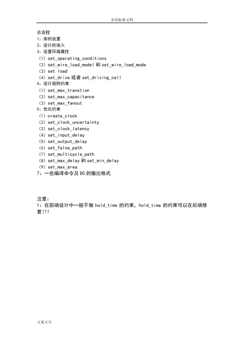
总流程1:库的设置2:设计的读入3:设置环境属性(1)set_operating_conditions(2)set_wire_load_model和set_wire_load_mode(3)set load(4)set_drive或者set_driving_cell4:设计规则约束(1)set_max_transtion(2)set_max_capacitance(3)set_max_fanout5:优化约束(1)create_clock(2)set_clock_uncertainty(3)set_clock_latency(4)set_input_delay(5)set_output_delay(6)set_false_path(7)set_multicycle_path(8)set_max_delay和set_min_delay(9)set_max_area7:一些编译命令及DC的输出格式注意:1:在前端设计中一般不做hold_time的约束,hold_time的约束可以在后端修复!!!总流程:1:对库进行基本设置,如下:设置完成后应该查看.synopsys_dc.setup里面库的设置和软件application setup处的设置是否一样!DC的初始化文件.synopsys.dc.setup需要用ls –a显示,命令:more .synopsys.dc.setup 查看文件内容!2:读入设计,两种方法:read和analyze+elaborateAnalyzer是分析HDL的源程序并将分析产生的中间文件存于work(用户可以自己指定)的目录下;Elaborate则在产生的中间文件中生成verilog的模块或者VHDL的实体缺省情况下,elaborate读取的是work目录中的文件中的第一个库的工作环境作为优化时使用的工作环境。
(1)set_operating_conditions:工作条件包括三方面—温度、电压以及工艺;工作条件一般分三种情况:best case, typical case, worst case图形界面:#1:先进入the symbol view of the top界面,选择top模块#2:attributes—operating environment—operating conditions命令方式:#1:可通过report_lib libraryname命令来查看,如下图查看的是slow.db库的工作条件,则使用命令:report_lib slow,右边是report_lib fast。
PSPICE_Orcad

输出变量的基本表达式
电压变量:
V(节点1)-节点1对地的电压, V(节点1,节点2)节点1、节点2间的电压 如:V(R1:1) - 也可V1(R1), V(R1:1,R1:2) V(Q2:C) - 也可VC(Q2) 对多端器件:V(Q4:B,Q4:C)-也可VBC(Q2)
电流变量:
I(元器件编号[:引出端名]) 如:I(Q1:C) - 也可IC(Q1) 对二端无源器件,不要给出引出端名,即: I(元器件编号)-规定电流从1端流进,2端流出,如: I(R1),I(C1) 对独立源, I(独立源编号),如:I(V1),规定电流从 正端流进,负端流出
RC1 10k C1 out1 5p RS1 V1 0Vdc 1k Q1 Q2N2222 Q2 Q2N2222 out2
RC2 10k
RS2 1k
0
Q3 Q2N2222 Q4 Q2N2222 V2 VDD 12V V3 VEE -12V VEE
0
0
直流工作点分析(Bias Point Detail)、直流灵敏度分析(DC Sensitivity)、直流传输特性分析(Transfer Function )可在同一 Profile中设置
例:1.23k、1.23E3和1230均表示同一个数。 特别注意:100meg=100e6,100m=100e-3
Pspice A/D中的单位 采用实用工程单位制,即:
时间单位为秒(s) 频率单位为赫兹(Hz) 电流单位为安培(A) 电压单位为伏特(V) 代表单位的字母可以省去,如表示470千欧 姆电阻: 470K, 4.7E5, 470KOhm
AC分析输出变量波形示例
1 15V 2 40 3 -0d
10V
20
- 1、下载文档前请自行甄别文档内容的完整性,平台不提供额外的编辑、内容补充、找答案等附加服务。
- 2、"仅部分预览"的文档,不可在线预览部分如存在完整性等问题,可反馈申请退款(可完整预览的文档不适用该条件!)。
- 3、如文档侵犯您的权益,请联系客服反馈,我们会尽快为您处理(人工客服工作时间:9:00-18:30)。
A Worst Case Timing Analysis Technique for Multiple-Issue MachinesSung-Soo Lim Dept.of Computer Engineering Seoul National UniversitySeoul,Korea,151-742Jung Hee HanDept.of Electrical Engineering and Computer Science University of Michigan,1301Beal Ave.Ann Arbor,MI48109-2122Jihong Kim Dept.of Computer Science Seoul National University Seoul,Korea,151-742Sang Lyul Min Dept.of Computer Engineering Seoul National UniversitySeoul,Korea,151-742AbstractWe propose a worst case timing analysis technique for in-order,multiple-issue machines.In the proposed tech-nique,timing information for each program construct is represented by a directed acyclic graph(DAG)that shows dependences among instructions in the program construct. From this information,we derive for each pair of instruc-tions the distance bounds between their issue ing these distance bounds,we identify the sets of instructions that can be issued at the same time.Deciding such in-structions is an essential task in reasoning about the timing behavior of multiple-issue machines.In order to reduce the complexity of analysis,the distance bounds are pro-gressively refined through a hierarchical analysis over the program syntax tree in a bottom-up fashion.Our experi-mental results show that the proposed technique can predict the worst case execution times for in-order,multiple-issue machines as accurately as ones for simpler RISC processors.1.IntroductionIn building a real-time system,the worst case execution times(WCETs)of tasks in the system should be predicted in advance since they are required in schedulability analysis for the system.Results of the WCET prediction should be both safe(i.e.,the predicted WCET should not be smaller than the real WCET)and accurate(i.e.,the difference between theover the program syntax tree in a bottom-up fashion.Asthe distance bounds of surrounding blocks are known dur-ing the hierarchical refinements,some adjacent instructions can be merged into a single node of the IDG if they have a constant distance.This merging step reduces the number of nodes maintained by the IDG,thus reducing the complexity of analysis.The proposed technique is described and validated using a simple in-order,multiple-issue machine model.Since the primary purpose of the work described in this paper is to understand whether the multiple-issue feature can be accu-rately analyzed to predict the WCETs of programs,we sig-nificantly simplify a machine model except for the multiple-issue capability.(This model is described in detail in Sec-tion3.)For the validation purpose,we build a timing tool based on the proposed technique using the multiple-issue machine model,and compare the WCET analysis results from the tool with measurements obtained using simulation. The results show that our technique can predict the WCETs for in-order,multiple-issue machines as accurately as ones for simple RISC processors based on the similar hierarchical technique[11].The rest of this paper is organized as follows.In Sec-tion2,we explain the ETS that forms the basis of the tech-nique proposed in this paper.In Section3,we describe our multiple-issue machine model used in this paper.An IDG is formally defined as well in this section.Section4presents the key algorithms to derive the distance bounds and to identify the instructions that can be issued simultaneously. In Section5,we explain how to augment the original ETS framework for the multiple-issue machine model using the distance bounds computed.Experimental results follow in Section6,and we conclude with future works in Section7.2.Extended Timing SchemaBefore we discuss the proposed technique,wefirst de-scribe the extended timing schema(ETS)on which our al-gorithms are based.The original timing schema is a set of formulas for reasoning about the timing behavior of vari-ous language constructs[14].The ETS extends the timing schema to reflect timing properties of modern architectural features such as pipelining and caching in two aspects:(1) redefinition of the timing information for each program con-struct and(2)redefinition of the timing formulas using newly introduced operations,concatenation()and pruning[11].In the ETS,each program construct is associated with a Worst Case Timing Abstract(WCTA)which is a data struc-ture containing information needed in hierarchical timing analysis.A program construct may have more than one execution path as an if statement and the WCETs of these execution paths differ significantly depending on preceding program constructs.Therefore,the worst case execution121S:while(exp)S1S:f(exp1,,exp)those in the else path,and the execution paths that cannot be the worst case execution path of the if statement are pruned.The timing formula for a loop statement with a loop bound models a loop unrolled times.This approach is exact but is computationally intractable for a large.In[11],Lim et al.give an efficient approximate loop timing analysis method using a maximum cycle mean algorithm due to Karp [9].In summary,in order to perform timing analysis withinthe ETS framework,the following three components should be decided:(1)determination of the PA structure,(2)def-inition of the operation on PAs,and(3)definition of the pruning condition.Once these three components are deter-mined,the worst case timing analysis of a program can be performed mechanically by traversing the program’s syntax tree in a bottom-up fashion and applying the timing formulas of the ETS.3.Multiple-Issue Machine Model and ProgramRepresentation3.1.Multiple-Issue Machine ModelThroughout this paper,we use a simple multiple-issue machine model with the following assumptions:Instructions are issued in the order shown in a program(in-order issue).However,each instruction can com-plete its execution regardless of other instructions’completion(out-of-order completion).The delayed branch scheme is used.For a branch in-struction,one delay slot is assumed.This assumptionis to ignore the effect of the branch prediction resultson the execution time.(A worst case timing analy-sis under branch prediction is one of our main futureresearch topics.)All memory accesses are cache hits.This assumptionis to ignore the effect of cache misses on the execu-tion time.(Since our approach does not make anyassumption on the cache system,previously proposedtechniques on the cache analysis[1,11,10]can easilybe integrated with our approach.)Processor can issue up to instructions simultane-ously,where is provided as a parameter to our anal-ysis.is equal to or smaller than the number offunctional units in the processor(i.e.,9in ourprocessor model).We further assume that our machine model has nine func-tional units as shown in Figure1and its instruction set is similar to that used in MIPS R3000/R3010[8].In Figure1,Figure1.Functional units of target processormodel.each functional unit is shown with the latency of operations performed by the corresponding functional unit.Both the Load/Store and Branch units are assumed to have one delay slot.3.2.Program RepresentationIn multiple-issue processors,the amount of exploitable parallelism is restricted by dependences among instructions. Such dependences include structural dependences(i.e.,re-source conflicts)and data dependences[7]1.Structural de-pendences are caused by multiple instructions competing for the same functional unit.On the other hand,data depen-dences are caused by multiple instructions that use the same register or memory location.In this paper,we introduce another type of dependences,order dependences,that are used to model that instructions are issued in-order in our machine model.To represent dependences among instructions,we use a directed acyclic graph(DAG),which we call an instruc-tion dependence graph(IDG).The IDG representation of a program is similar to popular DAG representation of a pro-gram used in compiler research[3,5].In an IDG,a node can represent either a single instruction or a sequence of instructions.In the proposed technique,each node of an IDG initially corresponds to a single instruction in a basic block.Through a hierarchical refinement process of our timing analysis technique,several nodes are merged into a single node which represents more than one instruction. Each edge=()of an IDG indicates that there is at least one non-redundant dependence between the instruction(s) represented by the node and the instruction(s)represented by the node.(The exact definition of redundant depen-dences is described below.)Each edge=()is associated with a weight(or)that represents the minimum cycles(c)(b)1765432 sll $25, $12, 0x2 ; $25 <- $12 << 2 lui $1, 0x1000 ; $1 <- 0x1000addu $1, $1, $25 ; $1 <- $1 + $25lwc1 $f18, 96($1) ; $f18 <- mem[$1 + 96]add.s $f18, $f18, $f18 ; $f18 <- $f18 + $f18add.s $f18, $f18, $f16 ; $f18 <- $f18 + $f16mul.s $f16, $f18, $f18 ; $f16 <- $f18 * $f18(a)Figure 2.An example program representa-tion.required between the issues of the first instructions of the nodes and .(For the description convenience,we use the issue of a node to mean the issue of the first instruction of a node.)As an example,consider the basic block shown in Fig-ure 2(a).The basic block contains a sequence of instructions based on the MIPS R3000/R3010instruction set.Among the instructions,sll ,lui ,and addu use the ALU functional unit,lwc1and add.s use the Float ALU functional unit,and mul.s uses the Float Multiply functional unit.The graph shown in Figure 2(b)represents all the dependences among the instructions including redundant dependences.In the dependence graph,since the weights for order depen-dences are all 0,they are not shown explicitly in the figure.Formally,we define that a dependence =()betweennodes andis redundant if one of the following two conditions is satisfied:(1)there exists another dependence =()between the same nodes and and (when there are more than one dependence with the same weight between the two nodes,we choose one arbitrarily among them),(2)there exists a set of dependences,=1,such that(i)1and1for 1and(ii).For example,because of rule (2),both of the two depen-dences between nodes 4and 6in Figure 2(b)are redundant.Figure 2(c)shows the corresponding IDG with the redun-dant dependences eliminated.In an IDG,since all redundant dependences were eliminated,there can be at most one edge between any pair of nodes.An IDG succinctly represents the timing-related informa-tion for a sequence of instructions.However,an IDG alone is generally not sufficient to predict the WCETs.While an IDG contains the complete information on the depen-dence relationship between the instructions represented by the IDG,more information from the surrounding blocks is necessary to predict the worst case issue patterns that result in the WCETs.For example,if the first instruction of the se-quence requires the Float Divide unit,its issue time can vary significantly depending on whether the Float Divide unit is used by the preceding instruction.This type of variation on the issue times makes it difficult to identify the instructions that can be issued simultaneously.To efficiently manage these difficulties,we divide IDG nodes into two types.For the first type of a node (called a resolved node ),each in-struction represented by the node knows which instructions in the same IDG use its functional unit and operands.For the second type of a node (called an unresolved node ),at least one instruction in the node cannot tell when its func-tional unit or operands may be used,simply by examining the preceding instructions in the same IDG.In our proposed technique,for unresolved nodes,we assume that their ex-ecutions may be delayed by the maximum possible delay for safe prediction.For accurate prediction,the maximum delay value is reduced as more information from surround-ing blocks are known through the hierarchical refinement process.Formally,we define the resolved and unresolved nodes as follows:Definition 1A node is said to use a register if the register is one of the source register(s)of an instruction in the node.Let use(i)for a node be the set of registers used by the instruction(s)in the node .Definition 2A node is said to define a register if the register is the destination register of an instruction in the node.Let def(i)for a node be the set of registers defined by the instruction(s)in the node .Definition 3A node is said to occupy a functional unit if an instruction in the node utilizes the functional unit during its execution.Let occupy(i)for a node be the set of functional units occupied by the instruction(s)in the node .Definition 4A node is said to be resolved if all the reg-isters in use(i)and def(i)are defined by preceding nodes inmul.s $f16,1 $12lwc1 $f18,sll $25, $12 3addu $1, $1, $25 796($1) add.s $f18, $f18, $f16add.s $f18, $f18, $f18 $f18, $f18 6 lui , 0x1000 , 0x2 45Figure 3.An IDG with resolved/unresolved nodes.the same IDG and all the functional units in occupy(i)are occupied by preceding nodes in the same IDG.Otherwise,the node is said to be unresolved.If a node is resolved,we say that all the dependences for the node are resolved.If a node is unresolved,we say that the node has unresolved dependences.Figure 3shows the same IDG used in Figure 2with the re-solved/unresolved information augmented.As an example of the unresolved nodes,consider node 4in the IDG.Wecan note that4=$1,4=$f18,and 4=Float ALU according to Definitions 1,2,and 3.Among the elements in 4and 4,register $f18is not defined by nodes 1,2,and 3.The functionalunit Float ALU in4is also not occupied by any of the preceding three nodes 1,2,and 3.Therefore,node 4is an unresolved node which has unresolved dependences for register $f18and the Float ALU functional unit.The dot-ted thick edge from outside of the IDG to node 4in Figure 3represents the unresolved dependence.Similarly,nodes 1,2,and 5are unresolved nodes as well due to unresolved dependences for registers or functional units.4.Distance Bounds between InstructionsIn this section,we first describe an algorithm for derivingthe distance bounds on the issue times of each pair of instruc-tions in a given IDG.(We call this a bounding step .)These distance bounds are used to identify the instructions that can be simultaneously issued.(We call this a multiple issuing step .)Once the distance bounds are computed for the IDG and the instructions are identified for multiple issues,the IDG can be simplified.(we call this a merging step .)For example,if two adjacent instructions have a constant issue distance,without loss of information,we can combine these two instructions into a single IDG node.The merging step reduces the complexity of analysis by reducing the number of nodes that need to be kept in an IDG.4.1.Definitions and TerminologyWe use the following terms and notations in explainingthe algorithms:We use the term resources to refer to both registers and functional units.Let 12be the set of resources in a processor model where is the total number of resources.is the sum of the number of registers and the number of functionalunits.(In our processor model,is 73,consisting of 64registers and 9functional units.)Each resource is associated with the maximum la-tency ,which is defined to be the maximum duration for which an instruction may occupy the resource .If is a functional unit,is the maximum instruc-tion latency among all the instructions that occupy during their executions.Let be the maximum for all the functional units.If an is a register,is defined as .For a given processor,’s can be obtained from the processor manual.In our proces-sor model,is 19cycles which is the latency of instructions for the Float Divide functional unit.For an unresolved node in an IDG,letbe the set of resources that are not resolved in node .The set consists of the registers and the functional units that are not resolved in node .The unresolved registers are the registers in or but not in for while the un-resolved functional units are the functional units inbut not in for .For each node ,is the time duration from the issue of the first instruction of node to the completion of the executions of all the in-structions in the node whileis the time duration from the issue of the first in-struction of node to the issue of the last instruction of node .is used to assign the maximum possible weight of an edge from node to a succeeding node andis to assign the minimum possible weight of an edge from node to a succeeding node.For eachnode ,is the maxi-mum of the maximum latencies of the resourcesin.is used to assign the maximum possible weight of an edge from a preceding node to node .4.2.Bounding StepIn order to represent the variation of instruction issue times,we derive the distance bounds between the issue times(b)(a)(c)max2Figure 4.A bounding step example.for each pair of nodes.As an example,consider the IDG shown in Figure 4(a)where nodes 1and 2have unresolved dependences.In order to compute the distance bounds for each pair of nodes,there are three combinations to consider:the distance bounds for nodes 1and 2,nodes 2and 3and nodes 1and 3.The lower bound for nodes 1and 2occurs when node 2is issued at the same time as node 1as shown in Figure 4(b).Such a scenario is possible because node 2has only an order dependence with node 1.Thus,the lower bound for nodes 1and 2is 0.On the other hand,the upper bound occurs when the issue of node 2is delayed as much as possible from the issue of node 1.Such a sce-nario is shown in Figure 4(c).In the figure,the black node represents the node that immediately precedes the current program construct.In this scenario,the black node is as-sumed to have only an order dependence with node 1,so it can be issued at the same time as node 1.Furthermore,we assume that the black node occupies the unresolved re-sources of node 2making the unresolved dependences of node 2be forced to be resolved.To give the upper bound,this unresolved dependence should have the largest possible latency,max 2,where is an element of the setof unresolved resources for node 2.Next,consider the bounds on the distance between nodes 2and 3.This distance is affected by three weights,23,13,and 12.The lower bound can be obviously 23(=3),but it can be tightened more.For instance,if the upper bound of the distance between nodes 1and 2is less than (1323)(=2),the distance between nodes 2and 3is guaranteed to be larger than 23(=3).Therefore,the lower bound is the larger of (1)23and (2)the difference between 13and the upper bound of the distance between nodes 1and 2.Similarly,the upper bound is the larger of (1)23and (2)the difference between 13and the lower bound of the distance between nodes 1and 2.These comparisons require the distance bounds between nodes 1and2to be calculated in advance.(b)(a)Figure 5.The bounding order.Finally,consider the distance bounds for nodes 1and 3.The lower bound can be obviously 13(=5).However,if the distance between nodes 1and 2is guaranteed to be larger than (1323)(=2),the distance between nodes 1and 3should be computed by summing the distance between nodes 1and 2and 23(=3).Therefore,the lower bound for nodes 1and 3is the larger of (1)13and (2)the sum of the lower bound of the distance between nodes 1and 2and 23.Similarly,the upper bound on the distance between nodes 1and 3is the larger of (1)13and (2)the sum of the upper bound of the distance between nodes 1and 2and 23.In calculating the distance bounds,some distance bounds must be computed earlier than others.For example,deriving the distance bounds for nodes 2and 3requires the distance bounds for nodes 1and 2to be available in advance.Sim-ilarly,deriving the distance bounds for nodes 1and 3also requires the distance bounds for nodes 1and 2to be avail-able in advance.This implies that deriving distance bounds should be performed in the order shown in Figure 5.Fig-ure 5(a)shows the order of calculating distance bounds with a sample IDG.The distance bounds for nodes 1and 2are cal-culated first followed by the calculation of distance bounds for nodes 2and 3,nodes 1and 3,and so on.Figure 5(b)shows the order of calculating distance bounds using a ta-ble whose cell represents the distance bounds between the row-numbered node and the column-numbered node.Generalizing the above example,we can compute the distance bounds between two nodes as follows.Let and be the minimum (required)and maximum (pos-sible)distances between the issue times of nodes and (i j),respectively.As shown in Figure 5,the calculation order is:[1212],[2323],[1313],[3434],[2424],[1414],.In calculating [],we consider the nodes that have dependences with node in the IDG.We classify such nodes into the following three classes according to their positions in the IDG as shown in Figure 6:(1)the nodes precedingnode (i.e.,nodes 12in Figure 6(b)),(2)node (Figure 6(c)),and (3)the nodes succeeding node (i.e.,(a)(b)(c)(d)Figure6.Three classes of nodes having de-pendences with node.nodes12in Figure6(d)).In order to calculate ,three candidate lower bound values from the three class are computed separately,and then the largest of three candidate values is chosen to be.For thefirst class, we calculate the differences between and where 1.is given in the original IDG andis calculated at an earlier stage.The largest of these dif-ferences is the candidate lower bound value from thefirst class.For the second class,is the candidate value.For the last class,we calculate the sums of and where 1.The largest of these sums is the candidate value from the third class.The maximum distance between the issue times of nodes and can be obtained when the issue of node is maximally delayed relative to node.For safe bound-ing on the maximum distance,we introduce additional edges (called max edges)between node1and the unresolved nodes of the IDG.The max edges between node1and unresolved node has a weight of,thus effectively models the maximum possible delay between a preceding(but yet unknown)node and unresolved node .Figure7(a)shows the IDG of Figure3with the max edges added.Note that the weights are all since the unresolved nodes have registers as their unresolved ing the modified IDG with the max edges,the calculation proceeds similarly to the calcu-lation.(In order to distinguish the modified IDG and the original IDG,we use to indicate a weight in the mod-ified IDG.is defined as follows:if1,if node is an unre-solved node and1,and0if there is no edge between nodes and in the IDG.)Three candidate up-per bound values from the three classes are computed and the largest value is selected as.For thefirst class, we calculate the differences between and where 1.The largest of these differences is the candi-date value from thefirst class.From the second class,we take as in the calculation.For the third class,we(a)[1, 19][1, 1][1, 17][2, 16][0, 0][4, 4](b)(c)Figure7.IDG modifications for calcula-tion and merging operation.calculate the sums of and where1. The largest of the sums is the candidate from the last class. The and calculations can be summarized by the following equations:max max1max1(1)max max1max1(2) Each equation in the above has three elements in the outer-most max operation and each element corresponds to each class of nodes.4.3.Multiple Issuing and Merging StepsIn the multiple issuing step,we identify the instructions that are guaranteed to be issued simultaneously,based on the distance bounds computed in the previous section,and then refine the distance bounds of the IDG to reflect the effect of identified instructions to the IDG representation.In principle,two nodes whose distance bounds are[0,0]can be issued simultaneously.If a series of nodes have the distance bounds of[0,0],these nodes can be potentially issued at the same time.However,the number of simultaneously issued instructions cannot be greater than the multiple-issue limit of a target processor.For example,in our machine model where the maximum of instructions can be issued simultaneously,consider a series of nodes1such that[11]=[0,0]for0. For the nodes,1,wefirst check if1. If1,all the nodes in the series are guaranteed to be issued at the same time and no special refinement step is necessary to reflect the effect of the multiple-issue identification.On the other hand,if1,not all the nodes in the series can be issued simultaneously.Since ourmachine model assumes an in-order issue,only thefirst nodes,11can be issued at the same time. The remaining nodes,,should be issued at least one cycle later than thefirst nodes.Therefore,in case that1,after identifying thefirst nodes,the IDG should be modified.To represent that only thefirst nodes can be issued simultaneously,we replace an edge between nodes1with an edge of a weight1.Since the new edge will change the distance bounds of the IDG, we recalculate the distance bounds for the affected nodes.A more detailed description on the multiple issuing algorithm can be found in[12].As it will be described in detail in the next section, an IDG is encoded into the PA structure that represents a program construct,and two successive IDGs are concate-nated into a new IDG during the hierarchical refinement process.Repeated concatenations,however,may require a large amount of space to maintain all the nodes of the con-catenated IDGs.Therefore,we propose a merging operation on an IDG that reduces the number of nodes in an IDG.(In our proposed technique,a merging operation is performed after the multiple issuing step.)Two adjacent nodes in an IDG are merged into a single node if the lower bound of the distance between two nodes are same as the upper bound of the distance between two nodes.That is,if1is equal to1,nodes and1can be merged into a single node.In general,nodes,11, can be merged into a single node(after the multiple issuing step)if[11]=[11],[1212]=[22],,[2121]=[11]and for1 1. Figure7(b)-(c)illustrates the merging operation.The IDG shown in Figure7(b)includes the distance bounds between nodes as well as the weights between nodes.In Figure7(b), the nodes that can be merged are shown inside a dotted box.For example,nodes2and3can be merged because the distance bounds between them are[1,1].Nodes5,6 and7can be merged as well because they have the distance bounds[0,0]and[4,4].Since merged nodes(except for thefirst node)have a constant distance on their issue times relative to thefirst node,no information is lost in predicting the WCETs by the merging operation.On the other hand, as the hierarchical analysis proceeds,the number of nodes that can be merged grows rapidly since most of unresolved nodes will be resolved during the hierarchical refinement process.Therefore,the reduction in the number of nodes by the merging operations is substantial.There are two more factors to consider during the merging operation.First,since the merged node represents several nodes before the merging operations are performed,we have to modify the weights between the merged node and other nodes in the merged IDG.(Note that our definition of a weight between two nodes means the minimumdistance[1,19][3,21][2,18][5,23][4,20][2,16](a)(b)M1M2M3M1M2M3M4 1234561652437[1,19][2,20][3,21][5,23][7,21][9,25][2,18][4,20][6,20][8,24][1,17][3,19][5,19][7,23][2,16][2,16][6,20][0,0][4,4][4,4][1,1]Figure8.A tabular form representation of dis-tance bounds.between the issues offirst instructions of the two nodes.) For example,in Figure7(c),the weight between merged nodes2and3is computed to be the sum of a constant distance between nodes2and3and the weight between nodes3and4in the original IDG.Second,even when a series of nodes have their distance bounds as[0,0],these nodes are not always merged for accurate prediction of the WCETs.This happens for the following two cases:(1) a series of nodes have distance bounds of[0,0],but the consecutive nodes start from thefirst node in the IDG and (2)a series of nodes have distance bounds of[0,0]but the last node in the IDG is also a part of these nodes.In thefirst case,if we merged the nodes,we will lose some accuracy when we concatenate with a preceding IDG whose last nodes have distance bounds[0,0].Similarly,in the second case,if we merged the nodes,we will lose some accuracy when we concatenate with a succeeding IDG whosefirst nodes have distance bounds[0,0].The distance bounds for all combinations of nodes in an IDG can be represented as a tabular form.Figure8shows the tabular form representations of the distance bounds for our example.Figure8(a)shows the distance bounds for original IDG and Figure8(b)shows the distance bounds after merging is applied to the IDG.This tabular representation is included into the PA structure for a program construct.5.Extensions to ETSIn this section,we describe the extensions made to the original ETS framework to support the WCET prediction for our multiple-issue machine model.We explain how to encode the IDG for a program construct in the PA structure and define the concatenation()operation and the pruning operation using the three distance bounds steps described in the previous section.The PA Structure To take into account the multiple-issue capability in the ETS framework,we define the PA structure of the program construct to include the IDG.To understand why an IDG is used instead of a reservation table which was used for simple pipelined processors,consider Figure9that。