KSE13003T中文资料
寻一款其他参数跟8050一样但电流在25A上下的NPN三极管知道

百度首页 | 百度知道 | 登录新闻网页贴吧知道 MP3 图片视频百科文库帮助 | 设置搜索答案我要提问我要回答百度知道 > 电子数码寻一款其他参数跟8050一样但电流在2.5A上下的NPN三极管浏览次数:921次悬赏分:5 | 解决时间:2010-2-7 22:54 | 提问者: zqw8604各位大哥帮帮忙吧最佳答案9011 NPN 30V 30mA 400mW 150MHz 放大倍数20-809012 PNP 50V 500mA 600mW 低频管放大倍数30-909013 NPN 20V 625mA 500mW 低频管放大倍数40-1109014 NPN 45V 100mA 450mW 150MHz放大倍数20-908050 NPN 25V 700mA 200mW 150MHz放大倍数30-1008550 PNP 40V 1500mA 1000mW 200MHz 放大倍数40-1409011 结构:NPN集电极-发射极电压 30V集电极-基电压 50V 射极-基极电压 5V集电极电流 0.03A耗散功率 0.4W结温 150℃特怔频率平均 370MHZ放大倍数:D28-45 E39-60 F54-80 G72-108 H97-146 I132-1989012 结构:PNP集电极-发射极电压 -30V集电极-基电压 -40V射极-基极电压 -5V集电极电流 0.5A耗散功率 0.625W结温150℃特怔频率最小 150MHZ放大倍数:D64-91 E78-112 F96-135 G122-166 H144-220 I190-3009013 结构:NPN集电极-发射极电压 25V集电极-基电压 45V射极-基极电压 5V集电极电流 0.5A耗散功率 0.625W结温 150℃特怔频率最小 150MHZ放大倍数:D64-91 E78-112 F96-135 G122-166 H144-220 I190-3009014 结构:NPN集电极-发射极电压 45V集电极-基电压 50V射极-基极电压 5V集电极电流 0.1A耗散功率 0.4W结温 150℃特怔频率最小 150MHZ放大倍数:A60-150 B100-300 C200-600 D400-10009015 结构:PNP集电极-发射极电压 -45V集电极-基电压 -50V射极-基极电压 -5V集电极电流 0.1A耗散功率 0.45W 结温 150℃特怔频率平均 300MHZ放大倍数:A60-150 B100-300 C200-600 D400-10009016 结构:NPN集电极-发射极电压 20V集电极-基电压 30V射极-基极电压 5V集电极电流 0.025A 耗散功率 0.4W结温 150℃特怔频率平均 620MHZ放大倍数:D28-45 E39-60 F54-80 G72-108 H97-146 I132-1989018 结构:NPN集电极-发射极电压 15V集电极-基电压 30V射极-基极电压 5V集电极电流 0.05A耗散功率 0.4W结温 150℃特怔频率平均 620MHZ放大倍数:D28-45 E39-60 F54-80 G72-108 H97-146 I132-198三极管85508550是一种常用的普通三极管。
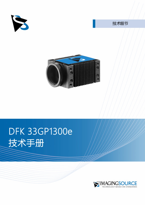
DFK 33GP1300e 技术手册说明书
技术细节1.要件速览 42.尺寸图 6 2.1DFK 33GP1300e 带脚架适配器的C型接口 (6)2.2DFK 33GP1300e 不带脚架适配器的C型接口 (7)2.3DFK 33GP1300e 带脚架适配器的CS型接口 (8)2.4DFK 33GP1300e 不带脚架适配器的CS型接口 (9)3.I/O 连接器 10 3.16-pin I/O 连接器 (10)3.1.1TRIGGER_IN (10)3.1.2STROBE_OUT (11)4.光谱特征 12 4.1红外截止滤波器 (12)4.2光谱灵敏度 - P1300 (12)5.相机控制 13 5.1传感器读出控制 (13)5.1.1像素格式 (13)8-Bit Bayer Raw (13)5.1.1.15.1.1.212-Bit Packed Bayer Raw (14)16-Bit Bayer Raw (14)5.1.1.35.1.1.4YUV 4:2:2 (14)5.1.1.5YUV 4:1:1 (14)5.1.1.6RGB24 (14)5.1.2分辨率 (15)5.1.3读出模式 (15)帧速率 (16)5.1.45.1.5局部扫描偏移 (17)5.2图像传感器控制 (18)5.2.1曝光时间 (18)5.2.2增益 (18)5.3自动曝光及增益控制 (19)5.3.1自动曝光 (19)自动增益 (19)5.3.25.3.3自动参考值 (20)5.3.4强光缩减 (20)5.3.5自动曝光限制 (20)5.3.6自动增益限制 (21)5.4触发 (21)触发模式 (21)5.4.15.4.2触发极性 (22)5.4.3软件触发 (22)5.4.4触发脉冲计数 (22)5.4.5触发源 (23)5.4.6触发重叠 (23)5.5触发定时参数 (23)触发延迟 (23)5.5.15.5.2触发去抖时间 (24)5.5.3触发遮罩时间 (24)5.5.4触发噪声抑制时间 (24)5.6数字I/O (25)5.6.1通用输入 (25)5.6.2通用输出 (25)5.7频闪 (26)5.7.1频闪启用 (26)5.7.2频闪极性 (26)频闪操作 (26)5.7.35.8白平衡 (26)5.8.1自动白平衡 (27)5.8.2白平衡模式 (27)5.8.3手动白平衡 (28)5.9图像处理 (29)5.9.1伽玛 (29)5.9.2查找表 (30)5.10色彩处理 (31)色调 (31)5.10.15.10.2饱和 (31)5.10.3色彩校正矩阵 (32)5.11自动功能感兴趣的区域 (34)5.11.1自动功能ROI启用 (34)5.11.2自动功能ROI预设 (34)5.11.3自动功能ROI自定义矩形 (35)5.12用户设置 (36)用户设置选择器 (36)5.12.15.12.2加载用户设置 (36)5.12.3保存用户设置 (36)默认用户配置 (37)5.12.46.R e v i s i o n H i story 381要件速览2尺寸图2.1DFK 33GP1300e 带脚架适配器的C型接口2.4DFK 33GP1300e 不带脚架适配器的CS型接口3I/O 连接器3.16-pin I/O 连接器相机后视图1开极闸M OS F E T最大限制0.2A(ID)!2启动电流最低条件3.5mA!3 G:地O:输出I:输入3.1.1TR IGG ER_I NTRIGGER_IN线可用于将曝光时间的开始与外部事件同步。
13003三极管参数,中文资料

13003三极管参数,中文资料13003三极管在整流器,充电器中很常用,对于了解13003三极管参数也显得很必要,下面为大家提供13003三极管的常用参数及应用电路图。
13003NPN型硅晶体管、功率开关三极管 主要应用于:日光灯、电子镇流器、充电器、等高压功率开关电路。
13003产品特性:芯片面积:1.63×1.63(特制芯片)额定电流:1.5 A(加大电流品种)饱和压降低、热性能好反向击穿电压高、漏电流小N型硅单晶三重扩散平面工艺制作 <<提示: 你觉得本站资料对你有帮助,请将网页加入浏览器收藏夹中,方便以后点击直接访问。
欢迎大家为容源电子网提供技术资料。
》温馨提示:将鼠标指针放在图片上,滚动鼠标可以动态改变图片大小,方便分析电路 型号与封装识别对照:HI13003: TO-251 (直插封装)HJ13003: TO-252 (贴片封装)HMJE13003T: TO-126 (半塑封)HMJE13003D: TO-126ML (全塑封)HMJE13003E: TO-220 (半塑封)你觉得本站资料对你有帮助,请将网页加入浏览器收藏夹中,方便以后点击直接访问。
欢迎大家为容源电子网提供技术资料。
》13003最大额定值温馨提示:将鼠标指针放在图片上,滚动鼠标可以动态改变图片大小,方便分析电路图。
<<提示: 你觉得本站资料对你有帮助,请将网页加入浏览器收藏夹中,方便以后点击直接访问。
欢迎大家为容源电子网提供技术资料。
》13003三极管应用电路图:>> 转载请注明出处并保留链接。
编辑:admin 时间:2014-1TAG标签: 整流器 三极管 芯片 高压 晶体管 镇流器 电路图 555 充电 制作【 复制本文地址及标题 】 【 在本地打印该网页 】 【 我要发表文章 】 【 返回上一页】分享到: QQ空间 新浪微博 开心网 人人网 更多...·上一篇: 应用交流接触器实现逆变器和市电自动切换·下一篇: 格力牌FGW-12远红外电暖器使用注意事项。
13003 MJE13003D 载带卷盘 - MOS-场效应管、晶体管

额定值 VALUE
850 500 9.0 1.0 2.0 2.0 4.0 1.0 150 -65~+150
单位 UNIT
V
A
W ℃
HAOHAI ELECTRONICS CO., LTD.
第1页 共5页 致力於中國功率器件優秀供應商
kkg@ 13003H: TO-251_TO-252
第2页 共5页 致力於中國功率器件優秀供應商
kkg@ 13003H: TO-251_TO-252
2A, 850V 特制高压 开关三极管 产品参数规格书
SOA(CD)
H13003H
High Voltage Switching Transister
Ptotoc Tj
hFE - IC
最小值 MIN
最大值 MAX
单位 UNIT
100 μA250来自8505009 V
0.5
1.2
1.0
7
20
35
4
■ 订单信息 ORDERING INFORMATION:
包装方式 PACKING
TO-251 普通袋装 NORMAL PACKING TO-251 条管装 NORMAL PACKING TO-252 条管装 NORMAL PACKING
IC=10mA, IE=0
VEBO
发射极-基极电压 Emitter- Base Voltage
IE=1mA, IC=0
Vcesat Vbesat
集电极-发射极饱和电压 Collector-Emitter Saturation Voltage
发射极-基极饱和电压 Base-Emitter Saturation Voltage
E-mail:kkg@
ST13003-K规格书
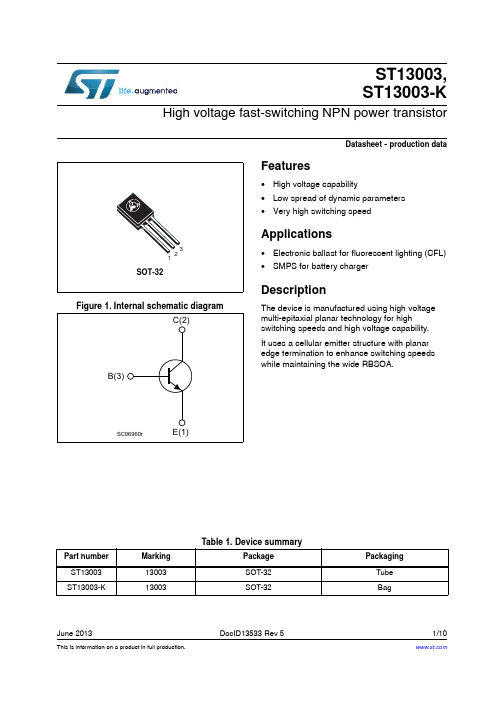
This is information on a product in full production.June 2013DocID13533 Rev 51/10ST13003, ST13003-KHigh voltage fast-switching NPN power transistorDatasheet - production dataFeatures•High voltage capability•Low spread of dynamic parameters •Very high switching speedApplications•Electronic ballast for fluorescent lighting (CFL)•SMPS for battery chargerDescriptionThe device is manufactured using high voltage multi-epitaxial planar technology for high switching speeds and high voltage capability.It uses a cellular emitter structure with planar edge termination to enhance switching speeds while maintaining the wide RBSOA.Table 1. Device summaryPart number Marking Package Packaging ST1300313003SOT-32Tube ST13003-K13003SOT-32BagElectrical ratings ST13003, ST13003-K2/10DocID13533 Rev 51 Electrical ratingsTable 2. Absolute maximum ratingsSymbol ParameterValue Unit V CES Collector-emitter voltage (V BE = 0)700V V CEO Collector-emitter voltage (I B = 0)400V V EBO Emitter-base voltage (I C = 0, I B = 0.75 A, t P < 10 μs)V (BR)EBOV I C Collector current1.5A I CM Collector peak current (t P < 5 ms)3A I B Base current0.75A I BM Base peak current (t P < 5 ms) 1.5A P TOT Total dissipation at T C = 25 °C 40W T STG Storage temperature-55 to 150°C T JOperating junction temperature-40 to 150°CTable 3. Thermal dataSymbol ParameterValue Unit R thJCThermal resistance junction-case max.3.1°C/WDocID13533 Rev 53/10ST13003, ST13003-K Electrical characteristics2 Electrical characteristicsT case = 25 °C unless otherwise specified.Table 4. Electrical characteristicsSymbol ParameterTest conditions Min.Typ.Max.Unit I CES Collector cut-off current(V BE = 0)V CE = 700 VV CE = 700 V T C = 125 °C15mA mA V (BR)EBO Emitter-Base breakdownvoltage (I C = 0)I E = 10 mA918V V CEO(sus) (1)1.Pulsed duration = 300 μs, duty cycle ≤ 1.5%Collector-emittersustaining voltage (I B = 0)I C = 10 mA400V V CE(sat) (1)Collector-emitter saturation voltage I C = 0.5 A I B = 0.1 A I C = 1 A I B = 0.25 A I C = 1.5 A I B = 0.5 A 0.511.5V V V V BE(sat) (1)Base-emitter saturation voltage I C = 0.5 A I B = 0.1 A I C = 1 A I B = 0.25 A 11.2V Vh FEDC current gain I C = 0.5 A V CE = 2 V I C = 1 A V CE = 2 V 852025t r t s t fResistive load Rise time Storage time Fall time V CC = 125 V I C = 1 A I B1 = 0.2 A I B2 = - 0.2 A t p = 25 μs140.7μs μs μst sInductive load Storage timeI C = 1 A I B1 = 0.2 A V BE = - 5 V L = 50 mH V Clamp = 300 V0.8μsElectrical characteristics ST13003, ST13003-K4/10DocID13533 Rev 52.1 Electrical characteristics (curves)Figure 4. Output characteristicsFigure 5. Reverse biased safe operatingST13003, ST13003-K Electrical characteristics Figure 8. Collector-emitter saturationFigure 9. Base-emitter saturation voltageDocID13533 Rev 55/10Electrical characteristics ST13003, ST13003-K6/10DocID13533 Rev 52.2 Test circuits1.Fast electronic switch2.Non-inductive resistor1.Fast electronic switch2.Non-inductive resistor3.Fast recovery rectifierST13003, ST13003-K Package mechanical data 3 Package mechanical dataIn order to meet environmental requirements, ST offers these devices in different grades ofECOPACK® packages, depending on their level of environmental compliance. ECOPACK®specifications, grade definitions and product status are available at: .ECOPACK® is an ST trademark.DocID13533 Rev 57/10Package mechanical data ST13003, ST13003-KTable 5. SOT-32 (TO-126) mechanical datamm.Dim.Min.Typ.Max.A 2.4 2.9B0.640.88B10.390.63D10.511.05E7.47.8e 2.04 2.29 2.54e1 4.07 4.58 5.08L15.316P 2.9 3.2Q 3.8Q11 1.52H2 2.15I 1.278/10DocID13533 Rev 5ST13003, ST13003-K Revision historyhistory4 RevisionTable 6. Document revision historyDate Revision Changes23-May-20071Initial release.09-Jul-20082Added Table1 on page1.15-Dec-20093Added Table3: Thermal data on page2.15-Jun-20114Modified: Table218-Jun-20135Added device ST13003.DocID13533 Rev 59/10ST13003, ST13003-KPlease Read Carefully:Information in this document is provided solely in connection with ST products. STMicroelectronics NV and its subsidiaries (“ST”) reserve the right to make changes, corrections, modifications or improvements, to this document, and the products and services described herein at any time, without notice.All ST products are sold pursuant to ST’s terms and conditions of sale.Purchasers are solely responsible for the choice, selection and use of the ST products and services described herein, and ST assumes no liability whatsoever relating to the choice, selection or use of the ST products and services described herein.No license, express or implied, by estoppel or otherwise, to any intellectual property rights is granted under this document. If any part of this document refers to any third party products or services it shall not be deemed a license grant by ST for the use of such third party products or services, or any intellectual property contained therein or considered as a warranty covering the use in any manner whatsoever of such third party products or services or any intellectual property contained therein.UNLESS OTHERWISE SET FORTH IN ST’S TERMS AND CONDITIONS OF SALE ST DISCLAIMS ANY EXPRESS OR IMPLIED WARRANTY WITH RESPECT TO THE USE AND/OR SALE OF ST PRODUCTS INCLUDING WITHOUT LIMITATION IMPLIED WARRANTIES OF MERCHANTABILITY, FITNESS FOR A PARTICULAR PURPOSE (AND THEIR EQUIVALENTS UNDER THE LAWS OF ANY JURISDICTION), OR INFRINGEMENT OF ANY PATENT, COPYRIGHT OR OTHER INTELLECTUAL PROPERTY RIGHT.ST PRODUCTS ARE NOT AUTHORIZED FOR USE IN WEAPONS. NOR ARE ST PRODUCTS DESIGNED OR AUTHORIZED FOR USE IN: (A) SAFETY CRITICAL APPLICATIONS SUCH AS LIFE SUPPORTING, ACTIVE IMPLANTED DEVICES OR SYSTEMS WITH PRODUCT FUNCTIONAL SAFETY REQUIREMENTS; (B) AERONAUTIC APPLICATIONS; (C) AUTOMOTIVE APPLICATIONS OR ENVIRONMENTS, AND/OR (D) AEROSPACE APPLICATIONS OR ENVIRONMENTS. WHERE ST PRODUCTS ARE NOT DESIGNED FOR SUCH USE, THE PURCHASER SHALL USE PRODUCTS AT PURCHASER’S SOLE RISK, EVEN IF ST HAS BEEN INFORMED IN WRITING OF SUCH USAGE, UNLESS A PRODUCT IS EXPRESSLY DESIGNATED BY ST AS BEING INTENDED FOR “AUTOMOTIVE, AUTOMOTIVE SAFETY OR MEDICAL” INDUSTRY DOMAINS ACCORDING TO ST PRODUCT DESIGN SPECIFICATIONS. PRODUCTS FORMALLY ESCC, QML OR JAN QUALIFIED ARE DEEMED SUITABLE FOR USE IN AEROSPACE BY THE CORRESPONDING GOVERNMENTAL AGENCY.Resale of ST products with provisions different from the statements and/or technical features set forth in this document shall immediately void any warranty granted by ST for the ST product or service described herein and shall not create or extend in any manner whatsoever, any liability of ST.ST and the ST logo are trademarks or registered trademarks of ST in various countries.Information in this document supersedes and replaces all information previously supplied.The ST logo is a registered trademark of STMicroelectronics. All other names are the property of their respective owners.© 2013 STMicroelectronics - All rights reservedSTMicroelectronics group of companiesAustralia - Belgium - Brazil - Canada - China - Czech Republic - Finland - France - Germany - Hong Kong - India - Israel - Italy - Japan - Malaysia - Malta - Morocco - Philippines - Singapore - Spain - Sweden - Switzerland - United Kingdom - United States of America10/10DocID13533 Rev 5。
T-13100中文资料
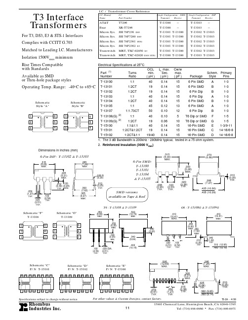
For other values & Custom Designs, contact factory.Specifications subject to change without notice.15801 Chemical Lane, Huntington Beach, CA 92649-1595Tel: (714) 898-0960 • Fax: (714) 896-0971RhombusIndustries Inc.11T3-2A - 4/99T3 Interface TransformersI.C. Manuf.I.C. Single Configuration - SMD Single Configuration - DIP NamePart Number Transmit Receive Transmit ReceiveAT&TT7296T-13100--T-13103--ExarXR-T7296T-13100--T-13103--Silicon Sys.SSI 78P236 DS3T-13101T-13100T-13102T-13103Silicon Sys.SSI 78P7200 DS3T-13101T-13100T-13102T-13103Silicon Sys.SSI 78P2361 STS1T-13101T-13100T-13102T-13103Silicon Sys.SSI 78P2362 E3T-13101T-13100T-13102T-13103Transwitch MRT, TXC-02050 E3T-13101T-13100T-13102T-13103Transwitch MRT, TXC-02020 DS3/STS1T-13100T-13100T-13103T-13103I.C. / Transformer Cross ReferenceElectrical Specifications at 25O C OCL L L max.Cw/w Part (1)Turns min.Sec. max.Schem.Primary Number Ratio ( µH )( µH )( pF )Package Style Pins T-131001:1400.1415 6 Pin SMD A 1-3T-131011:2CT 190.1415 6 Pin SMD B 1-3T-131021:2CT 190.1415 6 Pin Dip B 1-3T-131031:1400.1415 6 Pin Dip A 1-3T-131041:2CT 400.1415 6 Pin SMD B 1-3T-131051:1450.1213 6 Pin SMD A 1-3T-131071:1.73CT500.10126 Pin DipB1-3T-13108(G) (2)1:1400.105T6 Dip or SMD F 1-5T-13109(G)(2)1:2CT 190.0610T6 Dip or SMD G 1-5T-151001:1&1:1400.141516-Pin SMD E 1-3/9-11T-151011:2CT&1:2CT 190.141516-Pin SMD C 14-16/6-8T-151021:2CT&1:119/400.141516-Pin SMD D 14-16/6-8.015(0.38)TYP..505(12.83)MAX..016(0.41)TYP..205(5.21)MAX..360 (9.14).380 (9.65) .285(7.24)MAX..025(0.64)TYP..050(1.27)TYP..010(0.25)TYP..200(5.08)MAX..020(0.38).315(8.00)MAX..038(0.96)TYP..100(2.54)TYP.TYP..405 (10.29).425 (10.80) .270(6.86).286(7.27) .010(0.25)TYP.6-Pin SMD:T-13100T-13101T-13104& T-131051. The 3 dB Bandwidth is 200kHz - 280MHz typical, tested in a 75 ohm system.2. Reinforced Insulation (3000 V RMS )Schematic "F"T-13108Schematic "G"T-13109T6 : T-13108 & T-13109.350(8.89)MAX..250 MAX.(6.35).080(2.03).020 DIA.(0.51)TYP..120 (3.05)MIN..100(2.54)TYP..500(12.70)MAX..340(8.64).400(10.16)G6 : T-13108G & T-13109GMAX. .260(6.60)MAX..300(7.62)MAX..410 .020(0.51) .100(2.54)TYP..010(0.25).510 (12.95).480 (12.19)MAX..410(10.41).040(1.02)TYP.TYP.(10.41) TYP.SMD versionsavailable on Tape & ReelFor T3, DS3, E3 & STS-1 Interfaces Complies with CCITT G.703Matched to Leading I.C. Manufacturers Isolation 1500V RMS minimum Rise Times Compatiblewith StandardsAvailable as SMDor Thru-hole package stylesOperating Temp. Range: -40O C to +85OCSchematic "D"P/N T-15102Schematic "C"P/N T-15101Schematic "E"P/N T-15100.205(5.21)MAX.(0.30) TYP..012 .315(8.00)MAX..120(3.05)MIN..300(7.62) .285(7.24)MAX..020(0.51)TYP..100(2.54)TYP..050(1.27)TYP..010(0.25)TYP..008 R (0.20) .365(9.27)MAX.6-Pin DIP: T-13102 & T-13103Dimensions in Inches (mm)435621435621Schematic Style "A"Schematic Style "B"元器件交易网。
KSE13003H2ASTU;KSE13003TH2ATU;KSE13003TH1ATU;KSE13003H1ASTU;KSE13003H1AS;中文规格书,Datasheet资料
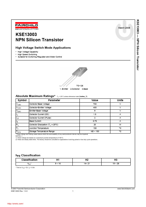
Figure 4. Switching Time
10
30
ICMAX. (pulse)
ms 10
25
s 1m
IC[A], COLLECTOR CURRENT
PC[W], POWER DISSIPATION
IC MAX. (DC)
1
s 5m
s 0m 10
20
15
0.1
10
5
0.01
0
1
10
100
1000
Figure 6. Power Derating
/
KSE13003 NPN Silicon Transistor
© 2007 Fairchild Semiconductor Corporation KSE13003 Rev. 1.0.0 4
hFE Classification
Classification
hFE*
* Test on VCE = 2V, IC = 0.5A.
H1
9 ~ 16
H2
14~ 21
H3
19 ~ 26
© 2007 Fairchild Semiconductor Corporation KSE13003 Rev. 1.0.0 1
* These ratings are limiting values above which the serviceability of any semiconductor device may be impaired. NOTES_1: 1) These ratings are based on a maximum junction temperature of 150°C. 2) These are steady state limits. The factory should be consulted on applications involving pulsed or low duty cycle operations.
三极管13003
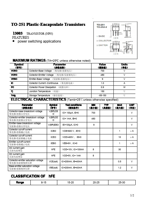
.TO-251Plastic-Encapsulate Transistors13003TRANSISTOR (NPN)FEATURESpower switching applicationsMAXIMUM RATINGS (TA=25℃unless otherwise noted)Symbol(符号)Parameter(参数名称)Value(额定值)Units(单位)VCBO Collector-Base Voltage (集电极-基极电压)700V VCEO Collector-Emitter Voltage (集电极-发射极电压)480V VEBO Emitter-Base Voltage (发射极-基极电压)9V IC Collector Current -Continuous (集电极电流) 1.0A PC Collector Power Dissipation (耗散功率)0.9W Tj Junction Temperature (结温)150℃TstgStorage Temperature (储存温度)-55-150℃ELECTRICAL CHARACTERISTICS (Tamb=25℃unless otherwise specified)Parameter (参数名称)Symbol (符号)Test conditions (测试条件)MIN(最小值)TYP (典型值)MAX (最大值)UNIT (单位)Collector-base breakdown voltage 集电极-基极击穿电压V(BR)CBO IC=100μA,IE=0700V Collector-emitter breakdown voltage 集电极-发射极击穿电压V(BR)CEO IC=1mA,IB=0480V Emitter-base breakdown voltage 发射极-基极击穿电压V(BR)EBO IE=100μA,IC=09V Collector cut-off current 集电极-基极截止电流ICBO VCB=600V ,IE=01μA Collector cut-off current 集电极-发射极截止电流ICEO VCE=400V ,IB=010μA Emitter cut-off current 发射极-基极截止电流IEBO VEB=9V ,IC=01μADC current gain 直流电流增益hFE VCE=10V,IC=100mA 830DC current gain 直流电流增益hFE VCE=5V,IC=1mA 8Collector-emitter saturation voltage 集电极-发射极饱和压降VCE(sat)IC=200mA,IB=40mA 0.5V Base-emitter saturation voltage 发射极-基极饱和压降VBE(sat)IC=200mA,IB=40mA1.2VCLASSIFICATION OF hFERange8-1515-2020-2525-30Typical Characteristics 13003I C , C o l l e c t o r C u r r e n t ( A )h F E - I Ch F E , D C C ur r e n t G a i nV C E sat - I CI c , C o l l e c t o r C u r r e n t ( A )V C E s a t (V ),C o l l e c t o r E m i t t e r S a t u r a t i o n V o l t a g eV B E s a t - I CI c , C o l l e c t o r C u r r e n t ( A )V B E s a t (V ), B a s e E m i t t e r S a t u r a t i o n V o l t a g e。
KSE13007中文资料
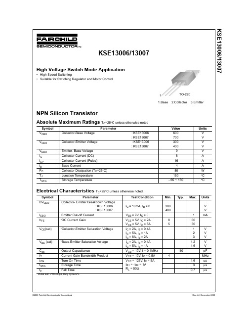
KSE13006/13007KSE13006/13007TRADEMARKSThe following are registered and unregistered trademarks Fairchild Semiconductor owns or is authorized to use and is not intended to be an exhaustive list of all such trademarks.ACEx™Bottomless™CoolFET™CROSSVOLT™E2CMOS™FACT™FACT Quiet Series™FAST®FASTr™GTO™HiSeC™ISOPLANAR™MICROWIRE™POP™PowerTrench®QFET™QS™Quiet Series™SuperSOT™-3SuperSOT™-6SuperSOT™-8SyncFET™TinyLogic™UHC™VCX™DISCLAIMERFAIRCHILD SEMICONDUCTOR RESERVES THE RIGHT TO MAKE CHANGES WITHOUT FURTHER NOTICE TO ANY PRODUCTS HEREIN TO IMPROVE RELIABILITY, FUNCTION OR DESIGN. FAIRCHILD DOES NOT ASSUME ANY LIABILITY ARISING OUT OF THE APPLICATION OR USE OF ANY PRODUCT OR CIRCUIT DESCRIBED HEREIN; NEITHER DOES IT CONVEY ANY LICENSE UNDER ITS PATENT RIGHTS, NOR THE RIGHTS OF OTHERS.LIFE SUPPORT POLICYFAIRCHILD’S PRODUCTS ARE NOT AUTHORIZED FOR USE AS CRITICAL COMPONENTS IN LIFE SUPPORT DEVICES OR SYSTEMS WITHOUT THE EXPRESS WRITTEN APPROVAL OF FAIRCHILD SEMICONDUCTOR INTERNATIONAL.As used herein:1. Life support devices or systems are devices or systems which, (a) are intended for surgical implant into the body, or (b) support or sustain life, or (c) whose failure to perform when properly used in accordance with instructions for use provided in the labeling, can be reasonably expected to result in significant injury to the user.2. A critical component is any component of a life support device or system whose failure to perform can be reasonably expected to cause the failure of the life support device or system, or to affect its safety or effectiveness.PRODUCT STATUS DEFINITIONSDefinition of TermsDatasheet Identification Product Status DefinitionAdvance Information Formative or InDesign This datasheet contains the design specifications for product development. Specifications may change in any manner without notice.Preliminary First Production This datasheet contains preliminary data, andsupplementary data will be published at a later date.Fairchild Semiconductor reserves the right to makechanges at any time without notice in order to improvedesign.No Identification Needed Full Production This datasheet contains final specifications. FairchildSemiconductor reserves the right to make changes atany time without notice in order to improve design. Obsolete Not In Production This datasheet contains specifications on a productthat has been discontinued by Fairchild semiconductor.The datasheet is printed for reference information only.。
KSE13005F
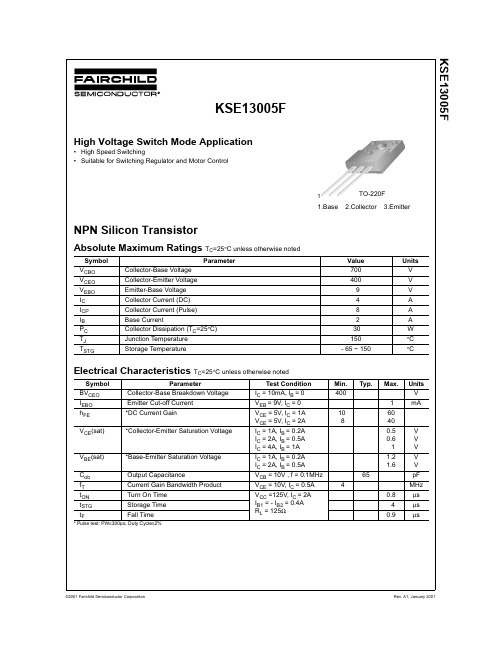
KSE13005FKSE13005FTRADEMARKSThe following are registered and unregistered trademarks Fairchild Semiconductor owns or is authorized to use and is not intended to be an exhaustive list of all such trademarks.DISCLAIMERFAIRCHILD SEMICONDUCTOR RESERVES THE RIGHT TO MAKE CHANGES WITHOUT FURTHER NOTICE TO ANY PRODUCTS HEREIN TO IMPROVE RELIABILITY, FUNCTION OR DESIGN. FAIRCHILD DOES NOT ASSUME ANY LIABILITY ARISING OUT OF THE APPLICATION OR USE OF ANY PRODUCT OR CIRCUIT DESCRIBED HEREIN;NEITHER DOES IT CONVEY ANY LICENSE UNDER ITS PATENT RIGHTS, NOR THE RIGHTS OF OTHERS.LIFE SUPPORT POLICYFAIRCHILD’S PRODUCTS ARE NOT AUTHORIZED FOR USE AS CRITICAL COMPONENTS IN LIFE SUPPORT DEVICES OR SYSTEMS WITHOUT THE EXPRESS WRITTEN APPROVAL OF FAIRCHILD SEMICONDUCTOR CORPORATION.As used herein:1. Life support devices or systems are devices or systems which, (a) are intended for surgical implant into the body,or (b) support or sustain life, or (c) whose failure to perform when properly used in accordance with instructions for use provided in the labeling, can be reasonably expected to result in significant injury to the user.2. A critical component is any component of a life support device or system whose failure to perform can be reasonably expected to cause the failure of the life support device or system, or to affect its safety or effectiveness.PRODUCT STATUS DEFINITIONS Definition of TermsDatasheet Identification Product Status DefinitionAdvance InformationFormative or In Design This datasheet contains the design specifications for product development. Specifications may change in any manner without notice.PreliminaryFirst ProductionThis datasheet contains preliminary data, andsupplementary data will be published at a later date.Fairchild Semiconductor reserves the right to make changes at any time without notice in order to improve design.No Identification Needed Full ProductionThis datasheet contains final specifications. Fairchild Semiconductor reserves the right to make changes at any time without notice in order to improve design.Obsolete Not In ProductionThis datasheet contains specifications on a product that has been discontinued by Fairchild semiconductor.The datasheet is printed for reference information only.ACEx™Bottomless™CoolFET™CROSSVOLT™DenseTrench™DOME™EcoSPARK™E 2CMOS™EnSigna™FACT™FACT Quiet Series™FAST ®FASTr™FRFET™GlobalOptoisolator™GTO™HiSeC™ISOPLANAR™LittleFET™MicroFET™MICROWIRE™OPTOLOGIC™OPTOPLANAR™PACMAN ™POP™PowerTrench ®QFET™QS™QT Optoelectronics™Quiet Series™SLIENT SWITCHER ®SMART START™Stealth™SuperSOT™-3SuperSOT™-6SuperSOT™-8SyncFET™TinyLogic™UHC™UltraFET ®VCX™。
KSE13003T中文资料
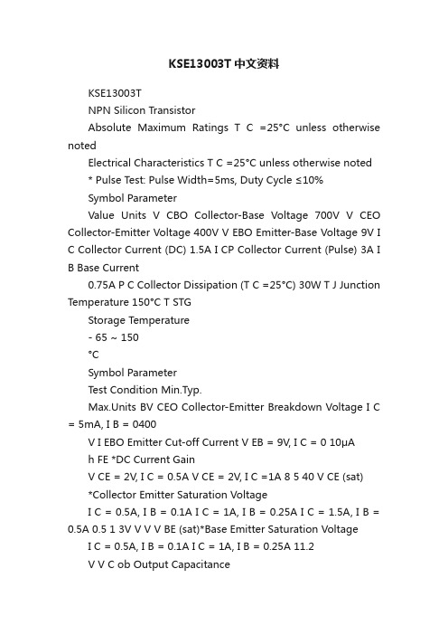
KSE13003T中文资料KSE13003TNPN Silicon TransistorAbsolute Maximum Ratings T C =25°C unless otherwise notedElectrical Characteristics T C =25°C unless otherwise noted * Pulse Test: Pulse Width=5ms, Duty Cycle ≤10%Symbol ParameterValue Units V CBO Collector-Base Voltage 700V V CEO Collector-Emitter Voltage 400V V EBO Emitter-Base Voltage 9V I C Collector Current (DC) 1.5A I CP Collector Current (Pulse) 3A IB Base Current0.75A P C Collec tor Dissipation (T C =25°C) 30W T J Junction Temperature 150°C T STGStorage Temperature- 65 ~ 150°CSymbol ParameterTest Condition Min.Typ.Max.Units BV CEO Collector-Emitter Breakdown Voltage I C = 5mA, I B = 0400V I EBO Emitter Cut-off Current V EB = 9V, I C = 0 10μAh FE *DC Current GainV CE = 2V, I C = 0.5A V CE = 2V, I C =1A 8 5 40 V CE (sat)*Collector Emitter Saturation VoltageI C = 0.5A, I B = 0.1A I C = 1A, I B = 0.25A I C = 1.5A, I B =0.5A 0.5 1 3V V V V BE (sat)*Base Emitter Saturation VoltageI C = 0.5A, I B = 0.1A I C = 1A, I B = 0.25A 11.2V V C ob Output CapacitanceV CB = 10V , f = 0.1MHz 21pF f T Current Gain Bandwidth Product V CE = 10V, I C = 0.1A 4MHz t ON Turn On Time V CC =125V, I C = 1A I B1 = 0.2A, I B2 = - 0.2A R L = 125?1.1μs t STG Storage Time 4.0μs t FFall Time0.7μs KSE13003THigh Voltage Switch Mode ApplicationsHigh Speed SwitchingSuitable for Switching Regulator and Motor Control1.Base2.Collector3.Emitter1TO-220KSE13003TKSE13003TTRADEMARKSThe following are registered and unregistered trademarks Fairchild Semiconductor owns or is authorized to use and is notintended to be an exhaustive list of all such trademarks.DISCLAIMERFAIRCHILD SEMICONDUCTOR RESERVES THE RIGHT TO MAKE CHANGES WITHOUT FURTHER NOTICE TO ANY PRODUCTS HEREIN TO IMPROVE RELIABILITY, FUNCTION OR DESIGN. FAIRCHILD DOES NOT ASSUME ANY LIABILITY ARISING OUT OF THE APPLICATION OR USE OF ANY PRODUCT OR CIRCUIT DESCRIBED HEREIN;NEITHER DOES IT CONVEY ANY LICENSE UNDER ITS PATENT RIGHTS, NOR THE RIGHTS OF OTHERS.LIFE SUPPORT POLICYFAIRCHILD’S PRODUCTS ARE NOT AUTHORIZED FOR USE AS CRITICAL COMPONENTS IN LIFE SUPPORT DEVICES OR SYSTEMS WITHOUT THE EXPRESS WRITTEN APPROVAL OF FAIRCHILD SEMICONDUCTOR INTERNATIONAL.As used herein:1. Life support devices or systems are devices or systems which, (a) are intended for surgical implant into the body,or (b) support or sustain life, or (c) whose failure to perform when properly used in accordance with instructions for use provided in the labeling, can be reasonably expected to result in significant injury to the user.2. A critical component is any component of a life support device or system whose failure to perform can be reasonably expected to cause the failure of the life support device or system, or to affect its safety or effectiveness.PRODUCT STATUS DEFINITIONS Definition of TermsDatasheet Identification Product Status DefinitionAdvance InformationFormative or In Design This datasheet contains the design specifications for product development. Specifications maychange in any manner without notice.PreliminaryFirst ProductionThis datasheet contains preliminary data, andsupplementary data will be published at a later date.Fairchild Semiconductor reserves the right to make changes at any time without notice in order to improve design.No Identification Needed Full ProductionThis datasheet contains final specifications. Fairchild Semiconductor reserves the right to make changes at any time without notice in order to improve design.Obsolete Not In ProductionThis datasheet contains specifications on a product that has been discontinued by Fairchild semiconductor.The datasheet is printed for reference information only.FACT?FACT Quiet series?FAST ?FASTr?FRFET?GlobalOptoisolator?GTO?HiSeC?I 2C?ImpliedDisconnect?ISOPLANAR?LittleFET?MicroFET?MicroP ak?MICROWIRE?MSX?MSXPro?OCX?OCXPro?OPTOLOGIC ?OPT OPLANAR?PACMAN?POP?Power247?PowerTrench ?QFET?QS?QT Optoelectronics?Quiet Series?RapidConfigure?RapidConnect?SILENT SWITCHER ?SMART START?SPM?Stealth?SuperSOT?-3SuperSOT?-6SuperSOT?-8SyncFET?TinyLogic?TruTranslation?UHC?UltraFET ?VCX?ACEx?ActiveArray?Bottomless?CoolFET?CROSSVOLT ?DOME?EcoSPARK?E 2CMOS?EnSigna?Across the board. Around the world.?The Power Franchise?Programmable Active Droop?。
13005 晶体管芯片说明书

█ 管芯示意图
█ 极限值(Ta=25℃)(封装形式:TO-220)
Tstg——贮存温度…………………………………… -55~150℃ Tj——结温………………………………………………… 150℃ PC——集电极功率耗散(Tc=25℃)……………………… 75W VCBO——集电极—基极电压……………………………… 700V VCEO——集电极—发射极电压…………………………… 400V VEBO——发射极—基极电压………………………………… 9V IC——集电极电流(DC)…………………………………… 4A IC——集电极电流(脉冲)………………………………… 8A IB——基极电流…………………………………………………2A
共基极输出电容
fT
特征频率
tON
导通时间
tSTG
载流子贮存时间
tF
下降时间
65 4
V IC=10mA,IB=0
1
mA VEB=9V,IC=0
40
VCE=5V,IC=1A
40
VCE=5V,IC=2A
0.5
V IC=1A,IB=0.2A
0.6
V IC=2A,IB=0.5A
1
V IC=4A,IB=1A
1.2
V IC=1A,IB=0.2A
1.6
V IC=2A,IB=0.5A
pF VCB=10V,f=0.1MHz
MHz VCE=10V,IC=0.5A
0.8
µs
4
ቤተ መጻሕፍቲ ባይዱ
µs
VCC=125V,IC=2A,
0.9
µs
IB1=-IB2=0.4A
Downloaded from electronic components distributor
SBN13003A中文资料

This device is designed for high voltage, high speed switching characteristic required such as lighting system, switching regulator, inverter and deflection circuit.
元器件交易网
SemiWell Semiconductor
SBN13003A
High Voltage Fast-Switching NPN Power Transistor
Features
- Very High Switching Speed (Typical 120ns@1.0A) - Minimum Lot-to-Lot hFE Variation - Low VCE(sat) (Typical 230mV@1.0A/0.25A) - Wide Reverse Bias S.O.A
SBN13003A
LC
f
IC
IB1
IB
VCE
D.U.T
RBB VBE(off)
VClamp
VCC
Resistive Load Switching Test Circuit RC
IC
IB1
VCE
IB
D.U.T
RBB
VCC
VBE(off)
5/6
元器件交易网
SBN13003A
Fig 6. Resistive Load Storage Time
10 ※ Notes : VCC = 125V hFE = 5 IB1 = - IB2
TJ = 25 oC
KSE13009F中文资料
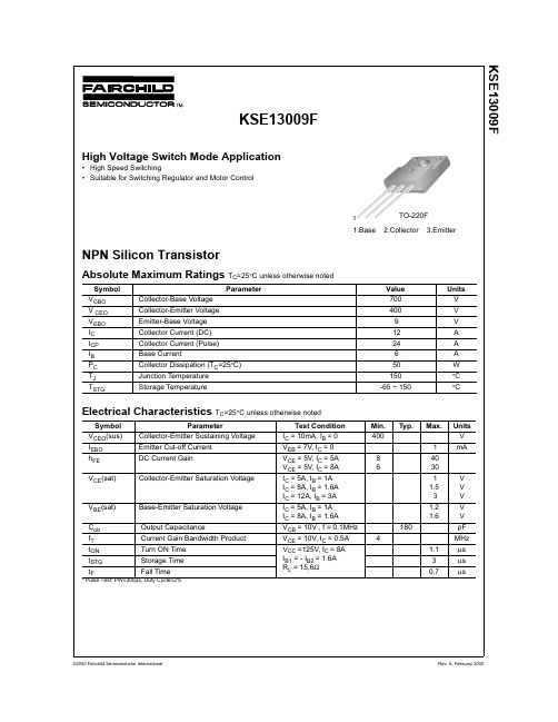
KSE13009FKSE13009FTRADEMARKSThe following are registered and unregistered trademarks Fairchild Semiconductor owns or is authorized to use and is not intended to be an exhaustive list of all such trademarks.ACEx™Bottomless™CoolFET™CROSSVOLT™E2CMOS™FACT™FACT Quiet Series™FAST®FASTr™GTO™HiSeC™ISOPLANAR™MICROWIRE™POP™PowerTrench®QFET™QS™Quiet Series™SuperSOT™-3SuperSOT™-6SuperSOT™-8SyncFET™TinyLogic™UHC™VCX™DISCLAIMERFAIRCHILD SEMICONDUCTOR RESERVES THE RIGHT TO MAKE CHANGES WITHOUT FURTHER NOTICE TO ANY PRODUCTS HEREIN TO IMPROVE RELIABILITY, FUNCTION OR DESIGN. FAIRCHILD DOES NOT ASSUME ANY LIABILITY ARISING OUT OF THE APPLICATION OR USE OF ANY PRODUCT OR CIRCUIT DESCRIBED HEREIN; NEITHER DOES IT CONVEY ANY LICENSE UNDER ITS PATENT RIGHTS, NOR THE RIGHTS OF OTHERS.LIFE SUPPORT POLICYFAIRCHILD’S PRODUCTS ARE NOT AUTHORIZED FOR USE AS CRITICAL COMPONENTS IN LIFE SUPPORT DEVICES OR SYSTEMS WITHOUT THE EXPRESS WRITTEN APPROVAL OF FAIRCHILD SEMICONDUCTOR INTERNATIONAL.As used herein:1. Life support devices or systems are devices or systems which, (a) are intended for surgical implant into the body, or (b) support or sustain life, or (c) whose failure to perform when properly used in accordance with instructions for use provided in the labeling, can be reasonably expected to result in significant injury to the user.2. A critical component is any component of a life support device or system whose failure to perform can be reasonably expected to cause the failure of the life support device or system, or to affect its safety or effectiveness.PRODUCT STATUS DEFINITIONSDefinition of TermsDatasheet Identification Product Status DefinitionAdvance Information Formative or InDesign This datasheet contains the design specifications for product development. Specifications may change in any manner without notice.Preliminary First Production This datasheet contains preliminary data, andsupplementary data will be published at a later date.Fairchild Semiconductor reserves the right to makechanges at any time without notice in order to improvedesign.No Identification Needed Full Production This datasheet contains final specifications. FairchildSemiconductor reserves the right to make changes atany time without notice in order to improve design. Obsolete Not In Production This datasheet contains specifications on a productthat has been discontinued by Fairchild semiconductor.The datasheet is printed for reference information only.。
- 1、下载文档前请自行甄别文档内容的完整性,平台不提供额外的编辑、内容补充、找答案等附加服务。
- 2、"仅部分预览"的文档,不可在线预览部分如存在完整性等问题,可反馈申请退款(可完整预览的文档不适用该条件!)。
- 3、如文档侵犯您的权益,请联系客服反馈,我们会尽快为您处理(人工客服工作时间:9:00-18:30)。
KSE13003TNPN Silicon TransistorAbsolute Maximum Ratings T C =25°C unless otherwise notedElectrical Characteristics T C =25°C unless otherwise noted* Pulse Test: Pulse Width=5ms, Duty Cycle ≤10%Symbol ParameterValue Units V CBO Collector-Base Voltage 700V V CEO Collector-Emitter Voltage 400V V EBO Emitter-Base Voltage 9V I C Collector Current (DC) 1.5A I CP Collector Current (Pulse) 3A I B Base Current0.75A P C Collector Dissipation (T C =25°C) 30W T J Junction Temperature 150°C T STGStorage Temperature- 65 ~ 150°CSymbol ParameterTest Condition Min.Typ.Max.Units BV CEO Collector-Emitter Breakdown Voltage I C = 5mA, I B = 0400V I EBO Emitter Cut-off Current V EB = 9V, I C = 0 10µAh FE *DC Current GainV CE = 2V, I C = 0.5A V CE = 2V, I C =1A 8 5 40 V CE (sat)*Collector Emitter Saturation VoltageI C = 0.5A, I B = 0.1A I C = 1A, I B = 0.25A I C = 1.5A, I B = 0.5A 0.5 1 3V V V V BE (sat)*Base Emitter Saturation VoltageI C = 0.5A, I B = 0.1A I C = 1A, I B = 0.25A 11.2V V C ob Output CapacitanceV CB = 10V , f = 0.1MHz 21pF f T Current Gain Bandwidth Product V CE = 10V, I C = 0.1A 4MHz t ON Turn On Time V CC =125V, I C = 1A I B1 = 0.2A, I B2 = - 0.2A R L = 125Ω1.1µs t STG Storage Time 4.0µs t FFall Time0.7µs KSE13003THigh Voltage Switch Mode Applications•High Speed Switching•Suitable for Switching Regulator and Motor Control1.Base2.Collector3.Emitter1TO-220KSE13003TKSE13003TTRADEMARKSThe following are registered and unregistered trademarks Fairchild Semiconductor owns or is authorized to use and is not intended to be an exhaustive list of all such trademarks.DISCLAIMERFAIRCHILD SEMICONDUCTOR RESERVES THE RIGHT TO MAKE CHANGES WITHOUT FURTHER NOTICE TO ANY PRODUCTS HEREIN TO IMPROVE RELIABILITY, FUNCTION OR DESIGN. FAIRCHILD DOES NOT ASSUME ANY LIABILITY ARISING OUT OF THE APPLICATION OR USE OF ANY PRODUCT OR CIRCUIT DESCRIBED HEREIN;NEITHER DOES IT CONVEY ANY LICENSE UNDER ITS PATENT RIGHTS, NOR THE RIGHTS OF OTHERS.LIFE SUPPORT POLICYFAIRCHILD’S PRODUCTS ARE NOT AUTHORIZED FOR USE AS CRITICAL COMPONENTS IN LIFE SUPPORT DEVICES OR SYSTEMS WITHOUT THE EXPRESS WRITTEN APPROVAL OF FAIRCHILD SEMICONDUCTOR INTERNATIONAL.As used herein:1. Life support devices or systems are devices or systems which, (a) are intended for surgical implant into the body,or (b) support or sustain life, or (c) whose failure to perform when properly used in accordance with instructions for use provided in the labeling, can be reasonably expected to result in significant injury to the user.2. A critical component is any component of a life support device or system whose failure to perform can be reasonably expected to cause the failure of the life support device or system, or to affect its safety or effectiveness.PRODUCT STATUS DEFINITIONS Definition of TermsDatasheet Identification Product Status DefinitionAdvance InformationFormative or In Design This datasheet contains the design specifications for product development. Specifications may change in any manner without notice.PreliminaryFirst ProductionThis datasheet contains preliminary data, andsupplementary data will be published at a later date.Fairchild Semiconductor reserves the right to make changes at any time without notice in order to improve design.No Identification Needed Full ProductionThis datasheet contains final specifications. Fairchild Semiconductor reserves the right to make changes at any time without notice in order to improve design.Obsolete Not In ProductionThis datasheet contains specifications on a product that has been discontinued by Fairchild semiconductor.The datasheet is printed for reference information only.FACT™FACT Quiet series™FAST ®FASTr™FRFET™GlobalOptoisolator™GTO™HiSeC™I 2C™ImpliedDisconnect™ISOPLANAR™LittleFET™MicroFET™MicroPak™MICROWIRE™MSX™MSXPro™OCX™OCXPro™OPTOLOGIC ®OPTOPLANAR™PACMAN™POP™Power247™PowerTrench ®QFET™QS™QT Optoelectronics™Quiet Series™RapidConfigure™RapidConnect™SILENT SWITCHER ®SMART START™SPM™Stealth™SuperSOT™-3SuperSOT™-6SuperSOT™-8SyncFET™TinyLogic™TruTranslation™UHC™UltraFET ®VCX™ACEx™ActiveArray™Bottomless™CoolFET™CROSSVOLT ™DOME™EcoSPARK™E 2CMOS™EnSigna™Across the board. Around the world.™The Power Franchise™Programmable Active Droop™。
