LVDS 基础_电子电路_工程科技_专业资料.ppt
LVDS原理及设计指南
LVDS原理及设计指南LVDS全称为低压差分信号(Low Voltage Differential Signaling),是一种高速串行接口技术,广泛应用于电子设备中进行高速数据传输。
LVDS主要通过两对差分信号进行数据传输,其中一对信号传输高电平信号,另一对信号传输低电平信号,通过差分运算来提高抗干扰能力和抗噪声能力,以实现高质量的数据传输。
LVDS的工作原理如下:1.发送端:将输入信号通过电流驱动压缩成低压差分信号,并通过双绞线传输给接收端。
2.传输线路:使用双绞线进行数据传输,利用差分运算来抵消传输线上的共模噪声和反射噪声。
3.接收端:对接收到的低压差分信号进行解码,还原成原始的输入信号。
设计LVDS接口时需要注意以下几点:1.信号线路的设计:为了保证信号的完整性和稳定性,需要控制信号线的阻抗匹配,减小信号线的长度和延迟,并避免信号线与高频噪声信号线的交叉和平行布线。
2.布线和PCB设计:保持信号线的长度均匀,并尽量使用同一层或相邻层进行差分信号线布线,以减小信号线之间的不平衡和串扰。
3.电源和接地:为了提供噪声的抑制和信号的稳定性,需要使用低噪声电源和低阻抗接地。
4.EMI抑制:由于LVDS接口传输速率高,会引起较大的电磁辐射干扰,因此需要在设计中加入适当的EMI抑制措施,如电磁屏蔽、地线设计和滤波器等。
5.信号匹配:为了保证所发送信号的完整性和稳定性,需要将发送端与接收端之间的差分阻抗匹配,以最大限度地减小信号反射和串扰。
总之,LVDS是一种高速串行接口技术,通过差分运算进行数据传输,具有抗噪声和抗干扰能力强的特点。
在设计LVDS接口时需注意信号线路的设计、布线和PCB设计、电源和接地、EMI抑制以及信号匹配等方面,以保证高质量的数据传输。
LVDS 基础

单路8bit LVDS
对于单路8bit LVDS接口,需要4对差分数据线,即RX0-和RX0+,RX1-和RX1+,RX2-和RX2 +,RX3-和RX3+。因每对差分数据线可以传输7bit数据,这样,4对差分数据线可以传输 4×7bit=28bit,除R0~R7、G0~G7、B0~B7占去24bit,还剩下4bit,HS、VS、DE占3bit, 还空余1 bit(若HS、VS信号不传输,将空余3bit)。
使用DU90124 单路24bit
24bit RGB输入,仅仅只有一路LVDS输出
因为只有一路LVDS输出,一个周期输出24位data。DE也是独立pin。 800*480*70=26880000pixs 26.88M*24bit=645.12Mbps
LVDS 简介
Sem.li
为何使用LVDS
LVDS接口又称RS644总线接口,1994年由美国国家半导体公司(NS)提出的为克服以TTL电平方式传输宽带高 码率数据时功耗大、EMI电磁干扰大等缺点而研制的一种视频信号传输模式,是一种电平标准,广泛应用于液晶屏 接口。 液晶显示器驱动板输出的数字信号是TTL信号,除了包括RGB数据信号外,还包括行同步、场同步、像素时钟等信 号,像素时钟信号的最高频率可超过28MHZ. 采用TTL接口,数据传输速率不高(一个CLK周期只能传输1bit数据),传输距离较短,且抗电磁干扰能力比较差, 会对RGB数据造成一定的影响。另外,TTL多路数据信号采用并行的传输方式,整个并口数量达几十路(RGB各8 位,8x3=24,加 DE,HSYNC,VSYNC,至少27位),不但连接不便,而且不适合超薄化的趋势。采用LVDS输出 接口传输数据,可以使这些问题迎刃而解,实现数据的高速率、低噪声、远距离、高准确度的传输。
LVDS信号原理及相关介绍 2013年7月2日

所以,LVDS具有高速、超低功耗、低噪声和低成本的优良特性。
3、差分信号抗噪特性 :
从差分信号传输线路上可以看出,若是理想状况,线路没有干扰时, 在发送侧,可以形象理解为:
噪声被抑止掉。
上述可以形象理解差分方式抑止噪声的能力。在实际芯片 中,是在噪声容限内,采用“比较”及“量化”来处理的。
LVDS接收器可以承受至少±1V的驱动器与接收器之间的地 的电压变化。由于LVDS驱动器典型的偏置电压为+1.2V,地的 电压变化、驱动器偏置电压以及轻度耦合到的噪声之和,在接 收器的输入端相对于接收器的地是共模电压。这个共模范围是: +0.2V~+2.2V。建议接收器的输入电压范围为:0V~+2.4V。
最基本的LVDS器件就是LVDS驱动器和接收器。LVDS的驱动器由驱动差分线对
的电流源组成,电流通常为3.5 mA。LVDS接收器具有很高的输入阻抗,因此驱
动器输出的大部分电流都流过100 Ω 的匹配电阻,并在接收器的输入端产生大 约350 mV的电压。当驱动器翻转时,它改变流经电阻的电流方向,因此产生有 效的逻辑“1”和逻辑“0”状态。
抑止共模噪声是DS(差分信号)的共同特性,采用差分平 衡传输,由于其电平幅度大,更不容易受干扰,适合工业现场 不太恶劣环境下通讯。
四、LVDS信号Vid的技术要求和测试方法:
五、实际应用中常见问题 :
1、PCB走线要求 :
2、PCB 过孔要求:
一般原则:对于高速信号,尽量减少过孔;信号速度低于 155Mbps,使用过孔也无妨; 对于表面贴片器件,其管脚的LVDS信号走线在PCB表层或者底层, 尽量使用“微带布线”方式,避免使用过孔联接信号; 对于插件器件,由于不使用过孔,其信号线本就可以联接到PCB 的“中间层”,这样一来,尽量使用“带状走线”,其性能更好。
LVDS信号的工作原理和特点 (2)
LVDS信号的工作原理和特点LVDS(Low Voltage Differential Signaling)是一种低电压差分信号传输技术,它通过在发送端将信号分成两路相反的电平来传输数据,接收端通过比较这两路信号的差值来恢复原始数据。
LVDS信号具有较高的抗干扰能力和传输速率,被广泛应用于各种数字信号传输领域。
一、LVDS信号的工作原理1. 发送端工作原理:LVDS发送端将输入的数字信号经过编码和差分放大处理,生成两路相反的电平信号。
这两路信号的差值表示了原始数据的逻辑状态,例如低电平差值表示“0”,高电平差值表示“1”。
发送端还会根据协议要求添加时钟信号,以确保接收端能够正确解析数据。
2. 接收端工作原理:LVDS接收端通过比较两路相反的电平信号的差值来恢复原始数据。
如果差值大于一个阈值,则被判定为“1”,如果差值小于阈值,则被判定为“0”。
接收端还会根据时钟信号对数据进行同步处理,以确保数据的准确传输和解析。
二、LVDS信号的特点1. 低电压差分传输:LVDS信号采用低电平差分传输技术,相较于单端传输,具有更好的抗干扰能力和传输稳定性。
差分信号的传输方式能够减少电磁辐射和噪声干扰,提高信号传输的可靠性和抗干扰能力。
2. 高传输速率:LVDS信号传输速率高,可以达到几百兆比特每秒(Gbps)甚至更高。
这使得LVDS广泛应用于高速数据传输领域,如显示器接口、视频传输、高速通信等。
3. 低功耗:LVDS信号传输时采用较低的电压和电流,因此具有较低的功耗。
这对于需要长距离传输或者挪移设备来说非常重要,可以延长电池寿命并提高系统效率。
4. 高抗干扰能力:由于采用了差分传输和编码技术,LVDS信号具有较强的抗干扰能力。
它能够有效抵御来自外部电磁场、噪声和干扰源的影响,确保信号传输的稳定性和可靠性。
5. 长距离传输:LVDS信号可以在较长的距离范围内传输,通常可以达到几十米甚至更远的距离。
这使得LVDS在需要远距离传输的应用中具有优势,如医疗设备、工业自动化等领域。
LVDS标准及介绍-(2)

LVDS1.0 LVDS简介LVDS(Low Voltage Differential Signaling)是一种低摆幅的差分信号技术,它使得信号能在差分PCB线对或平衡电缆上以几百Mbps的速率传输,其低压幅和低电流驱动输出实现了低噪声和低功耗.1.1 LVDS信号传输组成LVDS信号传输一般由三部分组成,如图1所示:差分信号发送器,差分信号互联器,差分信号接收器.图1 简单的单工LVDS接口连接图差分信号发送器:将非平衡传输的TTL信号转换成平衡传输的LVDS信号.通常由一个IC来完成.差分信号接收器:将平衡传输的LVDS信号转换成非平衡传输的TTL信号。
通常由一个IC来完成.差分信号互联器:包括联接线(电缆或者PCB走线),终端匹配电阻。
1.2 LVDS的工作原理图2 LVDS接口电路图如图2所示,LVDS驱动器由一个驱动差分线对的电流源组成(通常电流为3。
5mA),LVDS 接收器具有很高输入阻抗,因此驱动器输出的电流大部分都流过100Ω的匹配电阻,并在接收器的输入端产生生大约350mV的电压。
驱动器的输入为两个相反的电平信号,四个nMOS管的尺寸工艺是完全相同的.当输入为“1”时,标号IN+的一对管子导通,另一对管子截止,电流方向如图2,并产生大约350mV的压降;反之,输入为“0”时,电流反向,产生大约350mV的压降.这样根据流经电阻的电流方向,就把要传输的数字信号(CMOS信号)转换成了电流信号(LVDS信号)。
接受端可以通过判断电流的方向就得到有效的逻辑“1”和逻辑“0"状态。
从而实现数字信号的传输过程。
由于MOS管的开关速度很高,并且LVDS的电压摆幅低(350mV),因此可以实现高速传输.其电平特性如下图所示1.3 LVDS的国际标准LVDS是目前高速数字信号传输的国际通用接口标准,国际上有两个工业标准定义了LVDS:ANSI/TIA/EIA(American National Standards Institute/Telecommunications Industry Association/Electronic Industries Association)和IEEE(Institute for Electrical and Electronics Engineering)。
LVDS技术
DS36C200,DS90C031,DS90C031B,DS90C032, DS90C032B,DS90C402,DS90LT012A,DS90LT012AQ,DS90LV011A,DS90LV011AQ, DS90LV012A,DS90LV017A,DS90LV018A,DS90LV019,DS90LV027,DS90LV027A,DS90LV027AQ,DS90LV028A,DS90LV028AQ, DS90LV031A,DS90LV032A,DS90LV047A,DS90LV048A,DS90LV049,DS90LV049QAn Overview of LVDS TechnologyLiterature Number: SNLA165An Overview of LVDS TechnologyINTRODUCTIONRecent growth in high-end processors,multi-media,virtualreality and networking has demanded more bandwidth thanever before.But the point-to-point physical layer interfaceshave not been able to deal with moving information at thedata rates required.Some of today’s biggest challenges thatremain to be solved include:the ability to transfer data fast,lower power systems than currently available,and economi-cal solutions to overcome the physical layer bottleneck.DataTransmission standards like RS-422,RS-485,SCSI and oth-ers all have their own limitations most notably in transferringraw data across a media.Not anymore.Low Voltage Differ-ential Signaling(LVDS)is a high speed(>155.5Mbps),low power general purpose interface standard that solves thebottleneck problems while servicing a wide range of applica-tion areas.This application note explains the key advantages and ben-efits of LVDS technology.Throughout this application notethe DS90C031(LVDS5V Quad CMOS Differential LineDriver)and the DS90C032(LVDS5V Quad CMOS Differen-tial Line Receiver)will be used to illustrate the key points.Over50LVDS devices are offered currently(1998)from Na-tional,please refer to the LVDS device datasheets for com-plete specifications.STANDARDS OVERVIEWThere are two industry standards that define LVDS.Themore common of the two is the generic electrical layer stan-dard defined by the TIA.This standard is know as ANSI/TIA/EIA-644.The other application specific standard is an IEEE(Institute for Electrical and Electronics Engineering)standardtitled Scalable Coherent Interface(SCI).ANSI/TIA/EIA-644This standard was developed under the Data TransmissionInterface committee TR30.2.This standard defines driveroutput and receiver input characteristics.Functional specifi-cations and/or Protocols are not within the scope of the TlAstandard.It notes a recommended maximum data rate of655Mbps and a theoretical maximum of1.923Gbps basedon a loss-less media;however,maximum data rate is appli-cation(desired signal quality),and device specific(transitiontime).It is feasible that LVDS based interface will operate inthe500Mbps to1.5Gbps range in the near future.Minimummedia specifications are also defined within the standard.Italso discusses failsafe operation of the receiver under faultconditions and other configurations issues such asmulti-receiver operation.National Semiconductor held theeditor position for this standard.IEEE1596.3SCI-LVDSSCI originally referenced a differential ECL interface withinthe SCI(Scalable Coherent Interface)1596-1992IEEE stan-dard.But,this only addressed the high data rates requiredand did not address the low power concerns.Thus,SCI-LVDS was defined as a subset of SCI,and is specifiedin IEEE1596.3standard.SCI-LVDS specifies signaling lev-els(electrical specifications)for the high speed/low power physical layer interface.It also defines the encoding for packet switching used in SCI data transfers.Packets are constructed from2-byte(doublet)symbols.This is the funda-mental16-bit symbol size.No media is specified and the data rate can be in the order of500MT/s based on serial or parallel transmission of1,4,8,16,32,64,....bits.SCl-LVDS also supports RamLink for super low power data transmission in a restricted environment.The IEEE1596.3 standard was approved in March1994.National Semicon-ductor held the Chairperson position for this standard.SCI-LVDS is similar to the TIA version but differs in some electrical requirements and load conditions.Both standards feature similar driver output levels,receiver thresholds and data rates.The TIA version is the more generic of the two standards and is intended for multiple applications.LOW VOLTAGE DIFFERENTIAL SIGNALINGLVDS technology uses differential data transmission.The differential scheme has a tremendous advantage over single-ended schemes as it is less susceptible to common mode noise.Noise coupled onto the interconnect is seen as common mode modulations by the receivers and is rejected. The receivers respond only to differential voltages.LVDS technology is not dependent on a specific power sup-ply,such as+5V.This means there is an easy migration path to lower supply voltages such as+3.3V,+2.5V or even lower while still maintaining the same signaling levels and perfor-mance.Technologies like ECL or PECL are more dependent on the supply voltage.This feature is highly desirable in any application that foresees moving to lower supply voltages without substantial redesign or worrying about mixed voltage operation(+5V/+3.3V)on system boards.To achieve high data rate,low power and to reduce EMl ef-fects,signaling levels have to be reduced.The DS90C031/ DS90C032chipset’s limitation on data rate is mainly depen-dent on the technology driving the LVDS drivers.The aggregate bandwidth that LVDS technology can drive is in the Gbps range with a loss-less media.Data rates in the 500-1,000Mbps are possible and this limitation is primarily dependent on the media being driven.SIGNALING LEVELSAs the name implies,LVDS features a low voltage swing compared to other industry data transmission standards. The signaling levels are illustrated in Figure1,and a com-parison to PECL levels is also shown as reference.Because of the low swing advantage,LVDS achieves a high aggre-gate bandwidth in point-to-point applications.National has recently introduced a new family of parts called Bus LVDS. This family extends LVDS from point-to-point applications to multi-point applications is fully discussed in other National application notes.Bus LVDS features similar voltage swings, but provides increased drive current to handle double termi-nations required in multi-point applications.TRI-STATE®is a registered trademark of National SemiconductorCorporation.It is impossible to achieve high data rates and provide low power without utilizing low voltage swings.LVDS signaling levels are smaller(50%)than PECL levels as shown in Fig-ure1.EMI effects are also reduced as the signaling swings are much smaller than traditional CMOS,TTL or even PECL. This is due to the current mode drivers,the soft transitions, the low switching currents and the use of true differential data transmission.LVDS TERMINATIONLVDS uses a constant current mode driver to obtain its many features.The value of the current source for the DS90C031 is a maximum of4.5mA.The transmission media must be terminated to its characteristic impedance to prevent reflec-tions.Typically this is between100Ω–120Ωand is matched to the actual cable.A termination resistor is required to gen-erate the Differential Output Voltage(V OD)across the resis-tive termination load at the receiver input(see Figure2A). Data transmission from the driver to receiver without the ter-mination is not recommended.The simplicity of the LVDS termination scheme makes it easy to implement in most ap-plications.It is recommended to have a single100Ωtermina-tion between the driver outputs,and the use of surface mount components is also recommended to reduce the ef-fects of parasitics.The single resistor approach is the most common LVDS termination method because of its simplicity. Proper termination not only avoids reflection problems,but also reduces unwanted electromagnetic emissions.The user may also use a cable damping resistor with a ca-pacitor to ground as shown in Figure2B.This method pro-vides additional common mode termination.Due to the addi-tional complexity,this approach is not too common.ECL and PECL require more complex terminations than the “one”resistor solution for LVDS.PECL drivers typically re-quire220Ωpull down resistors from each driver output to ground along with the100Ωacross the driver outputs as shown in Figure2C.This termination method requires addi-tional PCB space and increases system cost compared to the single resistor LVDS termination.COMMON MODE RANGEAn LVDS receiver can tolerate a minimum of±1V ground shift between the driver’s ground and the receiver’s ground. Note that LVDS has a typical driver offset voltage of+1.2V, and the summation of ground shifting,driver offset voltage and any longitudinally coupled noise is the common mode voltage seen on the receiver input pins with respect to the re-ceiver ground.The common mode range of the receiver is +0.2V to+2.2V,and the recommended receiver input voltage range is from ground to+2.4V.For example,if a driver has a V OH of1.4V and a V OL of1.0V(with respect to the driver ground),and a+1V ground shift is present(driver ground +1V higher than receiver ground),this will become+2.4V (1.4+1.0)as V IH and+2.0V(1.0+1.0)as V IL on the receiver inputs referenced to the receiver ground(+2.2V V CM).Simi-larly,with a−1V ground shift and the same driver levels re-sults as0.4V(1.4−1.0)V IH and0.0V(1.0−1.0)V IL on the re-ceiver inputs(+0.2V V CM).This is shown graphically in Figure3.AN012326-1FIGURE1.PECL vs LVDS Signal Swing 2FAILSAFE FEATUREFailsafe is a receiver feature that guarantees the output to be in a known logic state (HIGH)under certain fault conditions.This occurs when the inputs of the receiver are either open,shorted or terminated.In some applications,not all receivers of the Quad DS90C032may be used.In this case,the unused receiver inputs should be left open.If the receiver does not support failsafe and the inputs are left open (See Figure 4),any ex-ternal noise above the receiver threshold can trigger the out-put and cause an error on the communication line.Since the DS90C032supports open input failsafe,the receiver output will provide an output High for this case.Another fault condition can occur if the inputs get acciden-tally shorted (See Figure 4).Under the above condition,the receiver output will also be at logic High and not in an un-known state.Another case could occur if the driver is either powered off,in TRI-STATE ®or even removed from the line while the re-ceiver stays powered on with inputs terminated by the 100Ωtermination resistor.The receiver output will provide a logic high under all the above mentioned conditions.Failsafe support is receiver de-vice dependent,please refer to the specific LVDS receiver datasheets to determine which level of failsafe support is provided.Remember that the receiver function is to amplify very small (mV),short duration (ps-ns)pulses to rail-to-railCMOS levels.System design should ensure that noise picked up on the interconnect is seen as common and not differential.This can be accomplished by using balanced cables,shielding from noise sources and closely-coupled dif-ferential traces on PCBs.POWER ON/OFF REQUIREMENTS and HIGH IMPEDANCE BUS PINSDepending upon the application high impedance bus pin may or may not be required.This refers to the loading effect of driver outputs and receiver inputs when power is off to the device.First generation LVDS parts were intended for use in point-to-point applications.In this configuration,when the driver is OFF,disabled,or unplugged,the link is down and no communication occurs.The bus loading effects of the device is of minor concern.The DS90C031/DS90C032family of de-vices have direct ESD protection pins on the bus pins.Even if a driver is active and a receiver is powered off,the output current is tightly limited and will not cause a latch-up condi-tion to occur on the receiver input.Second generation devices offered by National (DS90LV031A/DS90LV032A)are intended for a wider range of applications where high impedance bus pins may be re-quired.For this family of devices,the ESD protection cir-cuitry will not load the line when the device is powered off.To determine if a device supports high impedance bus pins,refer to the features list in the device datasheet and also theAN012326-2FIGURE 2.a,b,c.Termination SchemesAN012326-3FIGURE mon Mode Voltage Range3receiver input current parameters and the driver output leak-age parameters.National’s family of Bus LVDS parts also feature high impedance bus pins as they are intended for multi-drop and multi-point applications.POINT-TO-POINT CONFIGURATIONSFor interfaces where the transition time of the driver is sub-stantially shorter than the time delay of the media,the inter-connection must be considered a distributed load,not alumped load.The distributed elements of a transmission line(media)can greatly affect signal quality.More explicitly,transmission line theory dictates that if thetransition(rise or fall)time of the driver is less than four timesthe line delay,the media must be treated as a distributedload,not a lumped load,and careful attention must be paidto any impedance discontinuities and stubs.For a givendriver,if t r<4t d(where t r=driver rise time,t d=delay of the line)then the line should be considered as a lossy line.Thisis usually true if the t r of drivers are in the sub nanosecondrange.A quick calculation will clarify this rule of thumb.Forexample,the DS90C031driver has a typical t r of350ps,anda microstrip built with FR-4material has a t d of147ps for oneinch of PC trace.This calculates that,an inch of FR-4mi-crostrip will act as a transmission line(350<4*147)when driven by the DS90C031driver.Figure5includes a stub be-tween the termination resistor and the receiver input.This length must not be longer than one inch in length and should be kept as short as possible.Stub lengths of1inch or greater will cause the propagating signal to bounce off the high impedance end of the stubs and degrade the signal. Multiple reflections can travel up and down the line causing ringing,overshoot and undershoot which reduces the noise margin too.The fast t r of the DS90C031allows the driver to achieve ahigher bandwidth,but transmission line characteristics caneasily crop up on a system board if not handled properly atthese edge rates.To make the device work to its fullest capa-bility,the LVDS DS90C031and the DS90C032should be op-erated in a point-to-point configuration with minimum discon-tinuities on the transmission line.This ensures no stub problems on the line.The media must be terminated by a 100Ωline-to-line termination at the far end.A100Ωtermina-tion resistor terminates the two differential line in its charac-teristic impedance and also provides the differential voltage (V OD)for the current mode driver.Under the above condi-tions,the driver can drive a twp(twisted pair)wire over10m at speeds in excess of155.5Mbps(77.7MHz).Note that other LVDS devices offered by National support higher data rate operation.The FAST LVDS family of parts support400 Mbps operation,and the Channel Link family of LVDS parts operate even faster on the LVDS lines.BI-DIRECTIONAL APPLICATION ON ONE TWPIn a bi-directional application data can flow in only one direc-tion at a time(see Figure6)over the single twisted pair, however the bus needs to be terminated at both ends.This requires two100Ωterminating resistors,assuming the cable impedance is100Ω(one direction at a time).In Figure6,Rt1 terminates the signal when D1is driving,and Rt2terminates the signal when D2is driving.But,since the drivers are cur-rent mode(z4mA)devices,the two resistors in parallel will load down the driver(100Ω\100Ω=50Ω)which cuts the signal in half.This reduces system noise margin to only 25mV,as the minimum driver V OD is now125mV,and the receiver threshold is100mV.Since the driver output swing is severely attenuated due to dual parallel termination load,the bi-directional approach over one twp is not recommended with standard LVDS de-vices.Bus LVDS devices are recommended for use in appli-cations that employ two terminations(see AN-1115).AN012326-4FIGURE4.a,b,c.Failsafe Operation 4MULTI-DROP CONFIGURATIONIn a multi-drop configuration (see Figure 7),10receivers or more can be tied to the bus.Select an LVDS receiver that supports high impedance bus pins,if the devices use sepa-rate power supplies and some receivers may be powered off while communication is flowing from the driver to other pow-ered up receivers.Also,the stubs between the line and each receiver have the potential to create reflections if they are too long,or cause an impedance discontinuity.Remember that only one termination resistor should be used and it must be located at the far end of the cable.SIGNAL QUALITY ACROSS CABLEThere are numerous ways of determining signal quality on the transmission media.Bit Error Rate (BER),jitter,eye pat-tern,ratio of rise time and unit interval are some of the differ-ent ways designers use to determine signal quality.In this ar-ticle,eye patterns will be used to demonstrate signal quality for LVDS driver and receiver.In order to create an eye pattern,a PRBS (Pseudo Random Bit Sequence)of 511(29−1)bits NRZ data was used to drive the LVDS driver inputs.The LVDS driver was con-nected to a LVDS receiver with a 10m,25pair,28AWG,twp cable (SCSI grade cable).The eye was plotted on the differ-ential driver output at 155.5Mbps and also at the receiver in-put at the end of the cable (see Figure 8and Figure 9).A random data pattern is more prone to Inter Symbol Inter-ference (ISI).There is a greater chance of errors occurring from inter symbol interference as the duration of pulses get shorter and shorter.A bit arriving at the receiver input might not have enough time to cross the threshold before the ar-rival of the next bit,resulting in lost data.A PRBS with a pattern depth of 511bits or 2047(211−1)or 32767(215−1)was used to generate the eye pattern.The eye pattern is then used to characterize inter symbol interfer-ence issues.The opening of the eye determines the signal quality,and jitter can be measured at the crossing point.Other industry standards,SONET/SDH for example,speci-fies eye patterns for signal quality analysis.LVDS technology demonstrates a wide eye opening at 155.5Mbps over the 10m twp cable.Also refer to application note AN-808“Long Transmission Line and Data Signal Quality”for more discus-sions on signal quality.AN012326-7FIGURE 5.A Point-to-Point Configuration Using LVDSAN012326-8FIGURE 6.Bi-Directional Application overOne Pair of TwpAN012326-9FIGURE 7.Multi-Drop Configuration for LVDS5CONCLUSIONLVDS technology solves the ever increasing data rate prob-lem while decreasing power dissipation and can be widelyused in Telecom,Routers,Intelligent Hubs,LCD displays,Copiers and numerous other exciting applications.LVDStechnology provides the best solution for power budget re-quirements in today’s designs.This high speed interface al-lows designers to implement a simple point-to-point link with-out complex termination issues.Low power dissipation andthe use of a core process allows for the integration of PLLsand digital blocks to provide optimized interface single chipsolutions.LVDS technology provides solutions when Mega-bits at milliwatts are required.REFERENCESFor TIA standards contact:Global Engineering Documents/LIFE SUPPORT POLICYNATIONAL’S PRODUCTS ARE NOT AUTHORIZED FOR USE AS CRITICAL COMPONENTS IN LIFE SUPPORT DE-VICES OR SYSTEMS WITHOUT THE EXPRESS WRITTEN APPROVAL OF THE PRESIDENT OF NATIONAL SEMI-CONDUCTOR CORPORATION.As used herein:1.Life support devices or systems are devices or sys-tems which,(a)are intended for surgical implant intothe body,or(b)support or sustain life,and whose fail-ure to perform when properly used in accordancewith instructions for use provided in the labeling,canbe reasonably expected to result in a significant injuryto the user.2.A critical component in any component of a life supportdevice or system whose failure to perform can be rea-sonably expected to cause the failure of the life supportdevice or system,or to affect its safety or effectiveness.National SemiconductorCorporationAmericasTel:1-800-272-9959Fax:1-800-737-7018Email:support@National SemiconductorEuropeFax:+49(0)180-5308586Email:europe.support@Deutsch Tel:+49(0)180-5308585English Tel:+49(0)180-5327832Français Tel:+49(0)180-5329358Italiano Tel:+49(0)180-5341680National SemiconductorAsia Pacific CustomerResponse GroupTel:65-2544466Fax:65-2504466Email:sea.support@National SemiconductorJapan Ltd.Tel:81-3-5620-6175Fax:81-3-5620-6179AN012326-11FIGURE8.Eye Pattern at Driver OutputAN012326-12FIGURE9.Eye Pattern at Receiver Inputswith10m CableAN-971AnOverviewofLVDSTechnologyNational does not assume any responsibility for use of any circuitry described,no circuit patent licenses are implied and National reserves the right at any time without notice to change said circuitry and specifications.IMPORTANT NOTICETexas Instruments Incorporated and its subsidiaries(TI)reserve the right to make corrections,modifications,enhancements,improvements, and other changes to its products and services at any time and to discontinue any product or service without notice.Customers should obtain the latest relevant information before placing orders and should verify that such information is current and complete.All products are sold subject to TI’s terms and conditions of sale supplied at the time of order acknowledgment.TI warrants performance of its hardware products to the specifications applicable at the time of sale in accordance with TI’s standard warranty.Testing and other quality control techniques are used to the extent TI deems necessary to support this warranty.Except where mandated by government requirements,testing of all parameters of each product is not necessarily performed.TI assumes no liability for applications assistance or customer product design.Customers are responsible for their products and applications using TI components.To minimize the risks associated with customer products and applications,customers should provide adequate design and operating safeguards.TI does not warrant or represent that any license,either express or implied,is granted under any TI patent right,copyright,mask work right, or other TI intellectual property right relating to any combination,machine,or process in which TI products or services are rmation published by TI regarding third-party products or services does not constitute a license from TI to use such products or services or a warranty or endorsement e of such information may require a license from a third party under the patents or other intellectual property of the third party,or a license from TI under the patents or other intellectual property of TI.Reproduction of TI information in TI data books or data sheets is permissible only if reproduction is without alteration and is accompanied by all associated warranties,conditions,limitations,and notices.Reproduction of this information with alteration is an unfair and deceptive business practice.TI is not responsible or liable for such altered rmation of third parties may be subject to additional restrictions.Resale of TI products or services with statements different from or beyond the parameters stated by TI for that product or service voids all express and any implied warranties for the associated TI product or service and is an unfair and deceptive business practice.TI is not responsible or liable for any such statements.TI products are not authorized for use in safety-critical applications(such as life support)where a failure of the TI product would reasonably be expected to cause severe personal injury or death,unless officers of the parties have executed an agreement specifically governing such use.Buyers represent that they have all necessary expertise in the safety and regulatory ramifications of their applications,and acknowledge and agree that they are solely responsible for all legal,regulatory and safety-related requirements concerning their products and any use of TI products in such safety-critical applications,notwithstanding any applications-related information or support that may be provided by TI.Further,Buyers must fully indemnify TI and its representatives against any damages arising out of the use of TI products in such safety-critical applications.TI products are neither designed nor intended for use in military/aerospace applications or environments unless the TI products are specifically designated by TI as military-grade or"enhanced plastic."Only products designated by TI as military-grade meet military specifications.Buyers acknowledge and agree that any such use of TI products which TI has not designated as military-grade is solely at the Buyer's risk,and that they are solely responsible for compliance with all legal and regulatory requirements in connection with such use. TI products are neither designed nor intended for use in automotive applications or environments unless the specific TI products are designated by TI as compliant with ISO/TS16949requirements.Buyers acknowledge and agree that,if they use any non-designated products in automotive applications,TI will not be responsible for any failure to meet such requirements.Following are URLs where you can obtain information on other Texas Instruments products and application solutions:Products ApplicationsAudio /audio Communications and Telecom /communicationsAmplifiers Computers and Peripherals /computersData Converters Consumer Electronics /consumer-appsDLP®Products Energy and Lighting /energyDSP Industrial /industrialClocks and Timers /clocks Medical /medicalInterface Security /securityLogic Space,Avionics and Defense /space-avionics-defense Power Mgmt Transportation and Automotive /automotiveMicrocontrollers Video and Imaging /videoRFID OMAP Mobile Processors /omapWireless Connectivity /wirelessconnectivityTI E2E Community Home Page Mailing Address:Texas Instruments,Post Office Box655303,Dallas,Texas75265Copyright©2011,Texas Instruments Incorporated。
逻辑电平LVDS
在通用的电子器件设备中,TTL和CMOS电路的应用非常广泛。
但是面对现在系统日益复杂,传输的数据量越来越大,实时性要求越来越高,传输距离越来越长的发展趋势,掌握高速数据传输的逻辑电平知识和设计能力就显得更加迫切了。
1 几种常用高速逻辑电平1.1LVDS电平LVDS(Low Voltage Differential Signal)即低电压差分信号,LVDS接口又称RS644总线接口,是20世纪90年代才出现的一种数据传输和接口技术。
摘要LVDS、ECL、CML等是目前应用较多的几种用于高速传输的逻辑电平。
本文介绍每种逻辑电平的接口原理、特点、设计及应用场合,归纳比较它们的特性,最后举例说明不同逻辑电平之间的互连。
关键词LVDS ECL CML 逻辑电平在通用的电子器件设备中,TTL和CMOS电路的应用非常广泛。
但是面对现在系统日益复杂,传输的数据量越来越大,实时性要求越来越高,传输距离越来越长的发展趋势,掌握高速数据传输的逻辑电平知识和设计能力就显得更加迫切了。
1 几种常用高速逻辑电平1.1 LVDS电平LVDS(Low Voltage Differential Signal)即低电压差分信号,LVDS接口又称RS644总线接口,是20世纪90年代才出现的一种数据传输和接口技术。
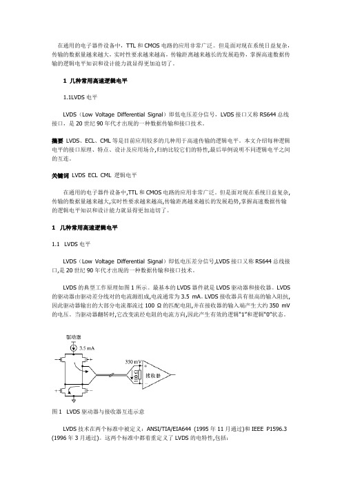
LVDS的典型工作原理如图1所示。
最基本的LVDS器件就是LVDS驱动器和接收器。
LVDS 的驱动器由驱动差分线对的电流源组成,电流通常为3.5 mA。
LVDS接收器具有很高的输入阻抗,因此驱动器输出的大部分电流都流过100 Ω的匹配电阻,并在接收器的输入端产生大约350 mV 的电压。
当驱动器翻转时,它改变流经电阻的电流方向,因此产生有效的逻辑“1”和逻辑“0”状态。
图1 LVDS驱动器与接收器互连示意LVDS技术在两个标准中被定义:ANSI/TIA/EIA644 (1995年11月通过)和IEEE P1596.3 (1996年3月通过)。
LVDS原理与应用

LVDS原理与应用简介1 LVDS信号介绍LVDS:Low Voltage Differential Signaling,低电压差分信号。
LVDS传输支持速率一般在155Mbps(大约为77MHZ)以上。
LVDS是一种低摆幅的差分信号技术,它使得信号能在差分PCB线对或平衡电缆上以几百Mbps的速率传输,其低压幅和低电流驱动输出实现了低噪声和低功耗。
IEEE在两个标准中对LVDS信号进行了定义。
ANSI/TIA/EIA-644中,推荐最大速率为655Mbps,理论极限速率为1.923Mbps。
1.1 LVDS信号传输组成TTL TTLLVDS差分接收器图1 LVDS信号传输组成图LVDS信号传输一般由三部分组成:差分信号发送器,差分信号互联器,差分信号接收器。
差分信号发送器:将非平衡传输的TTL信号转换成平衡传输的LVDS信号。
通常由一个IC来完成,如:DS90C031差分信号接收器:将平衡传输的LVDS信号转换成非平衡传输的TTL信号。
通常由一个IC来完成,如:DS90C032差分信号互联器:包括联接线(电缆或者PCB走线),终端匹配电阻。
按照IEEE规定,电阻为100欧。
我们通常选择为100,120欧。
1.2 LVDS信号电平特性LVDS物理接口使用1.2V偏置电压作为基准,提供大约400mV摆幅。
LVDS驱动器由一个驱动差分线对的电流源组成(通常电流为3.5mA),LVDS接收器具有很高的输入阻抗,因此驱动器输出的电流大部分都流过100Ω 的匹配电阻,并在接收器的输入端产生大约350mV 的电压。
电流源为恒流特性,终端电阻在100――120欧姆之间,则电压摆动幅度为:3.5mA * 100 = 350mV ;3.5mA * 120 = 420mV 。
下图为LVDS 与PECL (光收发器使用的电平)电平变化。
图2 LVDS 与PECL 电平图示由逻辑“0”电平变化到逻辑“1”电平是需要时间的。
LVDS接口电路基本原理
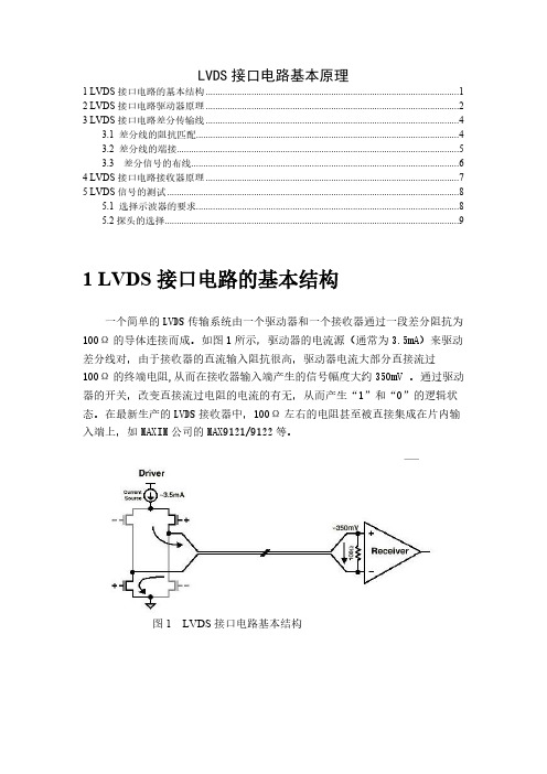
LVDS接口电路基本原理1 LVDS接口电路的基本结构 (1)2 LVDS接口电路驱动器原理 (2)3 LVDS接口电路差分传输线 (4)3.1 差分线的阻抗匹配 (4)3.2 差分线的端接 (5)3.3 差分信号的布线 (6)4 LVDS接口电路接收器原理 (7)5 LVDS信号的测试 (8)5.1 选择示波器的要求 (8)5.2探头的选择 (9)1 LVDS接口电路的基本结构一个简单的LVDS传输系统由一个驱动器和一个接收器通过一段差分阻抗为100Ω的导体连接而成。
如图1所示,驱动器的电流源(通常为3.5mA)来驱动差分线对,由于接收器的直流输入阻抗很高,驱动器电流大部分直接流过100Ω的终端电阻,从而在接收器输入端产生的信号幅度大约350mV 。
通过驱动器的开关,改变直接流过电阻的电流的有无,从而产生“1”和“0”的逻辑状态。
在最新生产的LVDS接收器中,100Ω左右的电阻甚至被直接集成在片内输入端上,如MAXIM公司的MAX9121/9122等。
图1 LVDS接口电路基本结构2 LVDS接口电路驱动器原理The Telecommunications Industry Association(TIA)颁布了一个标准,规定了用于转换二进制信号的LVDS接口电路的电气规格。
LVDS技术利用低电压差分信号来产生高速、低功率的数据传输。
差分信号的使用消除了共模噪声,因此确保了数据的传输速度以及抗噪性能。
如果想了解LVDS标准的详细信息,请查阅“Electrical Characteristics of Low Voltage Differential Signaling(LVDS)Interface Circuits”,TIA/EIA-644(March 1996)。
图2-1举例说明了一个通过一对差分连线115连接到一个LVDS接收器110的LVDS发生器100。
LVDS发生机100将一个数字的输入信号D_IN转换成为一对在差分输出终端TX_A和TX_B上的相反的LVDS输出信号。
LVDS基础介绍ppt课件
目前市场上上网本、家用电脑因持续降价 因素,在设计时均选择用铁氟龙线,优点:价 格较低,加工工艺简单。缺点EMI以及特性阻
抗不易管控。
同轴线一般用于高端商务笔记本,优点具 有良好的抗EMI效果,特性阻抗较稳定,高抗 Impr折ovi弯ng L性ive(s 同轴线每米价格是铁氟龙线7倍)9 。
3
Through medical innovation
Improving Lives
4
Through medical innovation
LVDS Cable 产品应用
Improving Lives
5
Through medical innovation
LVDS Cable 产品应用
Improving Lives
• 塑料本体: 1.使各接触弹片相互隔离,不能电性导通 2.固定各接触弹片 3.对各接触弹片进行机械保护 4.对各接触弹片进行工作环境遮蔽保护
•
Improving Lives
21
Through medical innovation
分类
•A焊接式es
D.内导体
内导体,最里面的铜丝,起传导作用,传 输高电平
Improving Lives
14
Through medical innovation
2、铁氟龙线(高温电子线)
Improving Lives
15
Through medical innovation
2、铁氟龙线线规
Improving Lives
料护套在电气装备用电线电缆產品中佔
了绝大多数。
Improving Lives
《VLSI设计基础》PPT课件 (2)

.2
h
24
2.2.2 CMOS与非门和或非门的结构及其等效 倒相器设计方法
1Y
1Y
2X
简单计算方法
2Y
Y μn X μp
2Y
2X
1X
1X
等效倒相器中(W/L) =X;(W/L) =Y
N
.2
h
P
25
2.2.2 CMOS与非门和或非门的结构及其等效 倒相器设计方法
.3
h
41
2.3.1 基本的集成电路加工工艺
器件制造基本问题
图形(版图) 窗口和屏蔽
图形转移 (光刻)
器
选择 掺杂
掺杂
件
材料沉积
和
电
互连
路
掺杂技术
图形(版图)
导线 绝缘
氧化及热处理
.3
h
42
2.3.1 基本的集成电路加工工艺
掩膜板(MASKS)
设计(软)
“底片”(硬)
单个电路图形
多个电路图形
.3
.2
h
19
2.2.2 CMOS与非门和或非门的结构及其等效 倒相器设计方法
.2
h
20
2.2.2 CMOS与非门和或非门的结构及其等效 倒相器设计方法
S/D
G
衬底
S/D G
MOSFET .2
D/S 衬底
D/S
数字逻辑等效电路模型 数字逻辑行为模型
h
21
2.2.2 CMOS与非门和或非门的结构及其等效 倒相器设计方法
对于并联网络结构,为保证在只有一个并联支路导通的情况下,仍能 获得所需的电阻,要求各并联支路等效晶体管宽长比与倒相器中对应 晶体管相同。
LVDS(低电压差分信号)原理简介

LVDS(低电压差分信号)原理简介LVDS(低电压差分信号)原理简介1 LVDS信号介绍LVDS:Low Voltage Differential Signaling,低电压差分信号。
LVDS传输支持速率一般在155Mbps(大约为77MHZ)以上。
LVDS是一种低摆幅的差分信号技术,它使得信号能在差分PCB线对或平衡电缆上以几百Mbps的速率传输,其低压幅和低电流驱动输出实现了低噪声和低功耗。
IEEE在两个标准中对LVDS信号进行了定义。
ANSI/TIA/EIA-644中,推荐最大速率为655Mbps,理论极限速率为1.923Mbps。
1.1 LVDS信号传输组成图1 LVDS信号传输组成图LVDS信号传输一般由三部分组成:差分信号发送器,差分信号互联器,差分信号接收器。
差分信号发送器:将非平衡传输的TTL信号转换成平衡传输的LVDS信号。
通常由一个IC来完成,如:DS90C031差分信号接收器:将平衡传输的LVDS信号转换成非平衡传输的TTL信号。
通常由一个IC来完成,如:DS90C032差分信号互联器:包括联接线(电缆或者PCB走线),终端匹配电阻。
按照IEEE规定,电阻为100欧。
我们通常选择为100,120欧。
1.2 LVDS信号电平特性LVDS物理接口使用1.2V偏置电压作为基准,提供大约400mV 摆幅。
LVDS驱动器由一个驱动差分线对的电流源组成(通常电流为3.5mA),LVDS接收器具有很高的输入阻抗,因此驱动器输出的电流大部分都流过100Ω的匹配电阻,并在接收器的输入端产生大约350mV 的电压。
电流源为恒流特性,终端电阻在100――120欧姆之间,则电压摆动幅度为:3.5mA * 100 = 350mV ;3.5mA * 120 = 420mV 。
下图为LVDS与PECL(光收发器使用的电平)电平变化。
图2 LVDS与PECL电平图示由逻辑“0”电平变化到逻辑“1”电平是需要时间的。
lvds概述
概述LVDS接口又称RS-644总线接口,是20世纪90年代才出现的一种数据传输和接口技术。
LVDS即低电压差分信号,这种技术的核心是采用极低的电压摆幅高速差动传输数据,可以实现点对点或一点对多点的连接,具有低功耗、低误码率、低串扰和低辐射等特点,其传输介质可以是铜质的PCB连线,也可以是平衡电缆。
LVDS在对信号完整性、低抖动及共模特性要求较高的系统中得到了越来越广泛的应用。
目前,流行的LVDS技术规范有两个标准:一个是TIA/EIA(电讯工业联盟/电子工业联盟)的ANSI/TIA/EIA-644标准,另一个是IEEE 1596.3标准。
1995年11月,以美国国家半导体公司为主推出了ANSI/TIA/EIA-644标准。
1996年3月,IEEE公布了IEEE 1596.3标准。
这两个标准注重于对LVDS接口的电特性、互连与线路端接等方面的规范,对于生产工艺、传输介质和供电电压等则没有明确。
LVDS可采用CMOS、GaAs或其他技术实现,其供电电压可以从+5V到+3.3V,甚至更低;其传输介质可以是PCB连线,也可以是特制的电缆。
标准推荐的最高数据传输速率是655Mbps,而理论上,在一个无衰耗的传输线上,LVDS的最高传输速率可达1.923Gbps。
LVDS接口的原理及电特性一个简单的LVDS传输系统由一个驱动器和一个接收器通过一段差分阻抗为100Ω的导体连接而成,如图1所示。
驱动器的电流源(通常为3.5mA)来驱动差分线对,由于接收器的直流输入阻抗很高,驱动器电流大部分直接流过100Ω的终端电阻,从而在接收器输入端产生的信号幅度大约350mV 。
通过驱动器的开关,改变直接流过电阻的电流的有无,从而产生“1”和“0”的逻辑状态。
在有些最新生产的LVDS接收器中,100Ω左右的电阻直接集成在片内输入端上了,如MAXIM公司的MAX9121/9122等。
在LVDS系统中,采用差分方式传送数据,有着比单端传输方式更强的共模噪声抑制能力。
