FT838NB_FT838RNA Application Note
碧云天RNAeasy动物RNA抽提试剂盒说明书
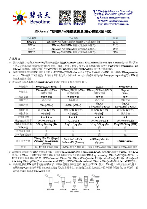
碧云天生物技术/Beyotime Biotechnology 订货热线: 400-1683301或800-8283301 订货e-mail :****************** 技术咨询: ***************** 网址: 碧云天网站 微信公众号RNAeasy ™动物RNA 抽提试剂盒(离心柱式)(试用装)产品简介:碧云天的离心柱式RNAeasy ™动物RNA 抽提试剂盒(RNAeasy ™ Animal RNA Isolation Kit with Spin Column)是一种基于离心柱法从动物组织或培养的动物细胞中安全、快速、便捷、稳定、高效、高质量地抽提长度大于200个核苷酸(nucleotide, nt)的RNA 的试剂盒。
抽提获得的大于200个核苷酸的RNA(也常被称为总RNA)可以用于各种常规用途。
本试剂盒抽提得到的RNA 可用于反转录、RT-PCR 、qPCR 、Northern 、点杂交(Dot Blot)、纯化mRNA 、体外翻译、RNase protection assay 、cDNA 克隆等下游实验;也可用于基因表达芯片分析(microarray)、高通量测序(high throughput sequencing)等对RNA 质量要求较高的情况。
碧云天的三款离心柱式及Trizol 法RNA 抽提试剂盒的主要特点和差异如下:动物组织或细胞中的RNA 按照长度可以分为长链RNA(long RNA)和小RNA(small RNA),长链RNA 通常大于200nt ,而小RNA 通常小于200nt 。
长链RNA 按照是否编码蛋白或多肽可以分为长链非编码RNA(long noncoding RNA, lncRNA)和mRNA 。
小RNA 主要包括非编码的5.8S rRNA(ribosomal RNA)、5S rRNA 、tRNA(transfer RNA)、microRNA(miRNA)、siRNA(small interfering RNA)、piRNA(Piwi-associated small RNA)、tsRNA(tRNA-derived small RNA)、srRNA(small rDNA-derived RNA)等。
AEMC PowerPad III Model 8336产品说明书
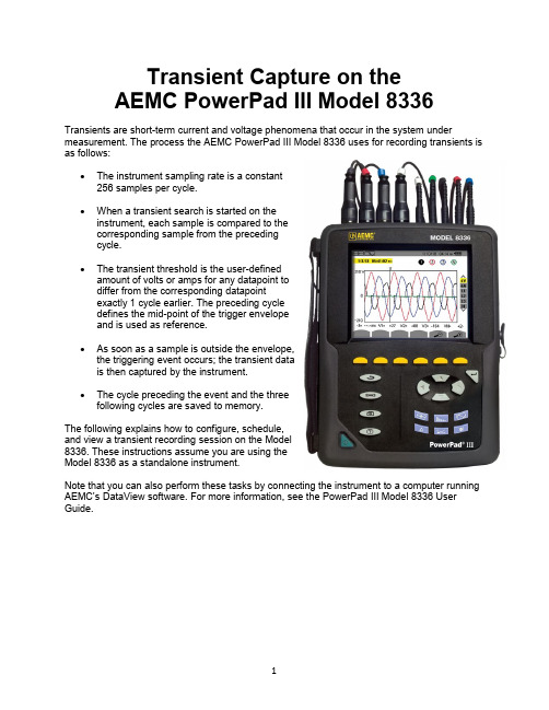
Transient Capture on theAEMC PowerPad III Model 8336Transients are short-term current and voltage phenomena that occur in the system under measurement. The process the AEMC PowerPad III Model 8336 uses for recording transients is as follows:•The instrument sampling rate is a constant256 samples per cycle.•When a transient search is started on theinstrument, each sample is compared to thecorresponding sample from the precedingcycle.•The transient threshold is the user-definedamount of volts or amps for any datapoint todiffer from the corresponding datapointexactly 1 cycle earlier. The preceding cycledefines the mid-point of the trigger envelopeand is used as reference.•As soon as a sample is outside the envelope,the triggering event occurs; the transient datais then captured by the instrument.•The cycle preceding the event and the threefollowing cycles are saved to memory.The following explains how to configure, schedule,and view a transient recording session on the Model8336. These instructions assume you are using theModel 8336 as a standalone instrument.Note that you can also perform these tasks by connecting the instrument to a computer running AEMC’s DataView software. For more information, see the PowerPad III Model 8336 User Guide.Transient Recording Configuration1. With the instrument turned ON, press the button to display the Waveform Capturescreen.2. Ensure Transient is highlighted, then press .●If there are no transient detection sessions stored in the instrument, the DetectionSchedule screen appears.●If there are recordings in the instrument, the Detection List screen is displayed. In thiscase, press to display the Detection Schedule screen.3. Press the function button under the icon to display the Voltage Thresholdsscreen. At the top of the screen is the Threshold Set-up field. Options are:●4V: The same voltage difference threshold applies to all phases and the neutral in theelectrical hook-up●3V+VN: One threshold applies to the phases and one applies to neutral●V1+V2+V3+V4: Each phase and neutral has its own assigned thresholdDepending on the electrical hook-up currently under measurement, not all these options may be available.4. The setting in this field determines which of the four fields below it (1, 2, 3, and N) areeditable:●4V: a single field is active for 1, 2, 3, and N.●3V+VN: one field is active for 1, 2, and 3; and another is active for N.●V1+V2+V3+N: each field is active.To edit a voltage threshold field, highlight it using the up and down arrow buttons, thenconfirm the selection by pressing . Use the left and right arrows to select a digit, and the up and down arrows to change it. You can also use these buttons to select units (V or kV).Press to confirm the edited field.5. Press the A button to display the Current Thresholds screen. This is similar to the VoltageThreshold screen. You can select which thresholds apply to which phases, and specify the value of the threshold (1mA through 9999kA). As with the voltage thresholds, not all these options may apply to all electrical hook-up types.Note that current transients typically occur frequently. We recommend performing a current transient search only when looking for a specific type of transient. At other times, such as when you are primarily interested in voltage transients, you can effectively disable current transient searching by setting the threshold to its maximum value.Scheduling Transient Detection1. Press the button to display the Waveform Capture screen.2. Ensure Transient is highlighted, then press .●If there are no transient detection sessions stored in the instrument, the DetectionSchedule screen appears.●If there are recordings in the instrument, the Detection List screen is displayed. In thiscase, press the button to display the Detection Schedule screen.3. This screen displays four input fields:●Start defines the time and date when the recording starts. This must be later than thecurrent date and time.●Stop specifies when the recording ends. This must be later than the start date and time.●Transient Count defines the maximum number of transients that you want to capturebefore stopping the session.●Name allows you to name the test. This can be 8 characters long.4. Use the arrow and buttons to highlight, select, and edit these fields.5. Press the button to write the settings to the instrument and start the session.6. If not enough memory is available, an error message appears informing you of this.Otherwise, the transient detection session will begin at the scheduled start time and date.If a session is scheduled but not yet started, the message DETECTION ON STANDBY appears on the screen until the start time is reached, at which point the message changes to DETECTION IN PROGRESS.When the session is active, the icon blinks at the top of the screen, along with a status bar showing the progress of the session. In addition, the (stop) button appears in place of .During the session, the Transient Count number is reduced by 1 every time a transient is recorded. If this number counts down rapidly and appears as though it will reach zero well before stop time is reached, we recommend stopping the session and setting the threshold to a higher, less sensitive value. The session will continue until: (1) you press , (2) the Transient Count limit is reached (see Step 3), or (3) the stop time/date is reached.7. When the transient detection session is finished, it appears in the Detection List screen. Youcan now open the session and view its contents, as explained in the following.Viewing a Transient Detection Session1. At the Detection Schedule screen, press the button.For all other displayed screens, press the button, and then select Transient.Either action displays the Detection List screen.2. If more than one transient detection recording is stored, use the arrows to select thedesired recording, then press to open it.In the preceding illustration:1 Location in the record of the zonedisplayed.4 Move cursor to transient triggering time.2 Instantaneous value of the signalsaccording to the position of the cursor on the scale. Use ◄ and ► to move cursor.5 Number assigned to displayed graph (e.g.1 is highlighted indicating channel V1 triggered capture of the transient)3 Move cursor to one period of the signalbefore transient triggering time. 6 Zoom In/Out。
RNA 6000 Nano Kit for 2100 Bioanalyzer Systems Qui
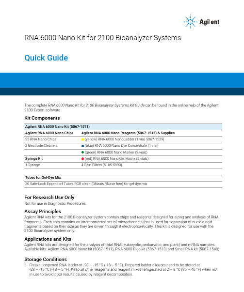
RNA 6000 Nano Kit for 2100 Bioanalyzer SystemsQuick GuideThe complete RNA 6000 Nano Kit for 2100 Bioanalyzer Systems Kit Guide can be found in the online help of the Agilent 2100 Expert software.Kit ComponentsAgilent RNA 6000 Nano Kit (5067-1511)Agilent RNA 6000 Nano Chips Agilent RNA 6000 Nano Reagents (5067-1512) & Supplies25 RNA Nano Chips (yellow) RNA 6000 NanoLadder (1 vial, 5067-1529)2 Electrode Cleaners (blue) RNA 6000 Nano Dye Concentrate (1 vial)(green) RNA 6000 Nano Marker (2 vials)Syringe Kit (red) RNA 6000 Nano Gel Matrix (2 vials)1Syringe 4 Spin Filters (5185-5990)Tubes for Gel-Dye Mix30 Safe-Lock Eppendorf Tubes PCR clean (DNase/RNase free) for gel-dye mixFor Research Use OnlyNot for use in Diagnostic Procedures.Assay PrinciplesAgilent RNA kits for the 2100 Bioanalyzer system contain chips and reagents designed for sizing and analysis of RNA fragments. Each chip contains an interconnected set of microchannels that is used for separation of nucleic acid fragments based on their size as they are driven through it electrophoretically. This kit is designed for use with the 2100 Bioanalyzer system only.Applications and KitsAgilent RNA kits are designed for the analysis of total RNA (eukaryotic, prokaryotic, and plant) and mRNA samples. Available kits: Agilent RNA 6000 Nano kit (5067-1511), RNA 6000 Pico kit (5067-1513) and Small RNA kit (5067-1548) Storage Conditions•Freeze unopened RNA ladder at -28–-15°C (-18–5°F). Prepared ladder aliquots need to be stored at -28–-15°C (-18–5°F). Keep all other reagents and reagent mixes refrigerated at 2–8°C (36–46°F) when not in use to avoid poor results caused by reagent decomposition.2•Protect dye and dye mixtures from light. Remove light covers only when pipetting. Dye decomposes when exposed to light.•Store the chips at room temperature.Equipment Supplied with the Agilent 2100 Bioanalyzer System•Chip priming station (5065-4401)•IKA vortex mixerAdditional Material Required (Not Supplied)•RNaseZAP® recommended for electrode decontamination and routine electrode cleaning •RNase-free water recommended for routine electrode cleaning•Pipettes (10µL and 1000µL) with compatible tips (RNase-free, no filter tips, no autoclaved tips)•0.5mL and 1.5mL microcentrifuge tubes (RNase-free)•Microcentrifuge ( 13000g)•Heating block or water bath for ladder/sample preparationSample preparationFor total RNA or mRNA analysis, the sample concentration must be within the specified range. If the concentration of your particular sample is above this range, dilute with RNase-free water.SpecificationsSetting up the Chip Priming Station1Replace the syringe:a Unscrew the old syringe from the lid of the chip priming station.b Release the old syringe from the clip. Discard the old syringe.c Remove the plastic cap of the new syringe and insert it into the clip.d Slide it into the hole of the luer lock adapter and screw it tightly to the chip priming station.2Adjust the base plate:a Open the chip priming station by pulling the latch.b Using a screwdriver, open the screw at the underside of the base plate.c Lift the base plate and insert it again in position C. Retighten the screw.Physical Specifications Analytical SpecificationsTotal RNA AssaymRNA Assay Analysis time30min Quantitative range 25–500ng/µL 25–250ng/µL Samples per chip 12Qualitative range 5–500ng/µL 5–250ng/µL Sample volume 1µL Sensitivity (S/N>3)5ng/µL in water25ng/µL in water Kit stability 4 months Quantitative precision (within a chip)10% CV 10% CV Kit size25 chips12 samples/chip = 300 samples/kitQuantitative accuracy11Determined analyzing the RNA ladder as sample20%20%Maximum salt concentration in sample100mM Tris 0.1mM EDTA or 125mM NaCl 15mM MgCl 2100mM Tris 0.1mM EDTA or 125mM NaCl 15mM MgCl 233Adjust the syringe clip:a Release the lever of the clip and slide it up to the top position.Essential Measurement Practices•Handle and store all reagents according to the instructions on the label of the individual box.•Avoid sources of dust or other contaminants. Foreign matter in reagents and samples or in the wells of the chip will interfere with assay results.•Allow all reagents to equilibrate to room temperature for 30min before use. Thaw samples on ice.•Protect dye and dye mixtures from light. Remove light covers only when pipetting. The dye decomposes when exposed to light and this reduces the signal intensity.•Always insert the pipette tip to the bottom of the well when dispensing the liquid. Placing the pipette at the edge of the well may lead to poor results.•Always wear gloves when handling RNA and use RNase-free tips, microcentrifuge tubes and water.•It is recommended to heat denature all RNA samples and RNA ladder before use for 2min and 70°C (once) and keep them on ice.•Do not touch the 2100 Bioanalyzer instrument during analysis and never place it on a vibrating surface.•Always vortex the dye concentrate for 10s before preparing the gel-dye mix and spin down afterwards.•Use a new syringe and electrode cleaners with each new kit.•Use loaded chips within 5min after preparation. Reagents might evaporate, leading to poor results.•To prevent contamination (e.g. RNase), it is strongly recommended to use a dedicated electrode cartridge for RNA assays.•Perform the RNase decontamination procedure for the electrodes daily before running any assays. Refer to the kit guide for details on electrode cleaning and decontamination.Agilent RNA 6000 Nano Assay ProtocolPreparing the RNA Ladder1Spin the ladder down and pipette in an RNase-free vial.2Heat denature the ladder for 2min at 70°C.3Immediately cool the vial on ice.4Prepare aliquots in recommended 0.5mL RNase-free vials with the required amount for typical daily use.5Store aliquots at -28–-15°C (-18–5°F). After initial heat denaturation, the frozen aliquots should not require repeated heat denaturation.6Before use, thaw ladder aliquots on ice (avoid extensive warming).Preparing the Gel1Pipette 550µL of RNA gel matrix (red ) into a spin filter.2Centrifuge at 1500 g ±20% for 10min at room temperature.3Aliquot 65µL filtered gel into 0.5mL RNase-free microcentrifuge tubes. Use filtered gel within 4 weeks. Store at2–8°C (36–46°F).Handling ReagentsThe dye can cause eye irritation. Because the dye binds to nucleic acids, it should be treated as a potential mutagen.Kit components contain DMSO. DMSO is skin-permeable and can elevate the permeability of other substances through the skin.✓Follow the appropriate safety procedures and wear personal protective equipment including protective gloves and clothes as well as eye protection.✓Follow good laboratory practices when preparing and handling reagents and samples.✓Always use reagents with appropriate care.✓For more information, refer to the material safety data sheet (MSDS) on .Agilent Technologies Inc. 2001-2022Printed in Germany, Edition: 11/2022*G2938-90037*Part No: G2938-90037 Rev. E.00Document No: SD-UF0000031 Rev. E.00Allow the RNA dye concentrate (blue ) to equilibrate to room temperatureVortex RNA dye concentrate (blue ) for 10µL of RNA marker (green ) in all 12sample wells and in the well marked.to find information on your local Contact Visit the Agilent website. It offers useful information, support, and current developments about the products and /en/product/automated-electrophoresis/bioanalyzer-systems .Put a new RNA chip on the chip priming station.µL of gel-dye mix in the well marked .mL and then close the chip priming µL of gel-dye mix in the wells marked .µL of prepared ladder in well marked .Pipette 1µL of sample in each of the 12 sample wells. Pipette 1(green ) in each unused sample well.Put the chip horizontally in the IKA vortexer and vortex for 1 9 µl gel-dye 9 µl gel-dye1 µl ladder 1 µl sample5 µl marker。
FTDI USB转串口芯片产品说明书
Future Technology Devices International Ltd (FTDI)Unit 1, 2 Seaward Place, Centurion Business Park, Glasgow, G41 1HH, United KingdomTel.: +44 (0) 141 429 2777 Fax: + 44 (0) 141 429 2758E-Mail(Support):************************:Neither the whole nor any part of the information contained in, or the product described in this manual, may be adapted or reproduced in any material or electronic form without the prior written consent of the copyright holder. This product and its documentation are supplied on an as-is basis and no warranty as to their suitability for any particular purpose is either made or implied. Future Technology Devices International Ltd will not accept any claim for damages howsoever arising as a result of use or failure of this product. Your statutory rights are not affected. This product or any variant of it is not intended for use in any medical appliance, device or system in which the failure of the product might reasonably be expected to result in personal injury. This document provides preliminary information that may be subject to change without notice. No freedom to use patents or other intellectual property rights is implied by the publication of this document. Future Technology Devices International Ltd, Unit1, 2 Seaward Place, Centurion Business Park, Glasgow, G41 1HH, United Kingdom. Scotland Registered Number: SC136640Future Technology Devices International LtdUSB-COM485-PLUS2DatasheetDocument Reference No.: FT_000136Version 1.2Issue Date: 2010-04-121Introduction1.1Functional DescriptionThe USB-COM485-PLUS2 is a USB to a dual interface RS485 level serial UART adaptor incorporating FTDI’s FT2232H Hi-Speed USB2.0 (480Mb/s) to dual serial UART interface IC device. The FT2232H handles all the USB signaling and protocols. The adaptor provides a fast, simple way to connect devices with an RS485 interface to USB.USB-COM485-PLUS2 is a USB to a dual-port RS485 adapter.The integrated electronics of the USB-COM485-PLUS2 utilise the FTDI FT2232H and includes RS485 level shifters plus TXD/RXD LEDs to provide a visual indication of data traffic through the module.Figure 1.1 USB-COM485-PLUS2The module uses a standard USB-B device connector for connection to an upstream host or hub port.RS485-level signals are available on an industry-standard DE-9P connector. The maximum RS485-level data rate is 10Mbps.The USB-COM485-PLUS2 module requires USB device drivers, available free from , which are used to make the USB-COM485-PLUS2 appear as a Virtual COM Port (VCP). This allows existing serial communications software, such as HyperTerminal, to exchange data through the USB-COM485-PLUS2 to a legacy RS485 peripheral device.1.2LED DescriptionThe USB-COM485-PLUS2 uses three LEDs to indicate a valid link as well as data traffic according to the following table:1.3Block Diagram1.3.1Block descriptionUSB B Client ConnectorThis connector provides the interface for connection to a USB Host or Hub port. The maximum cable length is 5 meters, according to the USB 2.0 specification.FTDI FT2232HFT2232H Hi-Speed USB2.0 (480Mb/s) is a dual serial UART interface IC device. Operating system device drivers are required in order to work with the one to provide the Virtual COM Port serial functionality. Dual RS485 Level ShifterThe RS485 level shifter converts the signals provided by the FT2232H into the voltage levels required by RS485 devices.DE-9P Connector (Male)The DE-9P connector is configured in an industry standard (TIA/EIA-574) pin-out to provide connection to RS485 peripherals through standard cables. See section 3.1.21.4FeaturesAdds dual RS-485 serial port by connecting to a USB 2.0 Hi-Speed interface.Easy plug & play installation and RS-485 device connectionOperates with USB 1.1 & 2.0 Host and Hub portsIndustry Standard FTDI chip set & device drivers for maximum compatibilityMicrosoft Windows ®WHQL-certified, Mac OS X, Linux and Windows CE device driversInstalls as a standard Windows COM portCOM port number can be changed to any available COM port number, to support HyperTerminal,or any other serial communications software application running in WindowsSupports Windows Server 2008, 2003, Vista, XP, 2000, Windows CE, Linux, Mac OS XFIFO: 4K byte transmit buffer, 4K byte receive bufferRS-485 data signals: Data+, Data-, GNDPowered by USB port. No external power adapter required. +5V output available.Serial port speed up to 10MbpsSerial Communication Parameterso Parity: None, Even, Odd o Data bits: 7, 8oFlow control: X-ON/X-OFF, NoneTwo DE-9P male connectorLEDs indicate USB Enumeration, RxD, TxD for monitoring port status & easy diagnosticsOperating temperature of -40°C to +85°CEcho and non-Echo two modes can be selected.1.5 Performance Figures1Introduction (1)1.1Functional Description (1)1.2LED Description (2)1.3Block Diagram (2)1.3.1Block description (2)1.4Features (3)1.5Performance Figures (3)2Installation (6)2.1Example Applications and Configurations (6)2.1.1Wiring (6)2.2Device Driver Installation (7)2.2.1Microsoft Windows (7)2.2.2Mac OS X, Linux, Windows CE (11)3Connections (12)3.1External Connectors (12)3.1.1USB (12)3.1.2RS485 (13)4Electrical details (14)4.1USB (14)4.2RS485 (14)4.3Power Output (14)5Mechanical Details (15)5.1Module Mechanical Dimensions (15)6Physical Environment Details (16)6.1Storage (16)6.2Operating (16)7Environmental Approvals & Declarations (17)7.1EMI Compatibility (17)7.2Safety (17)7.3Environmental (17)7.4Reliability (17)7.4.1MTTF (17)7.5Import / Export Information (18)8Troubleshooting (19)8.1Hardware (19)8.2Device Driver (19)9Contact Information (20)10Appendix A - List of Figures and tables (22)Appendix B - Revision History (23)2Installation2.1Example Applications and Configurations2.1.1WiringInsert the A-plug into an available USB Host or Hub port. Insert the mini-B-plug into the USB mini-B-receptacle on the USB-COM485-PLUS2.Table 2.1 – RS485 DTE to DCE connectionFigure 2.1 USB-COM485-PLUS2 Termination resistor and echo disable2.2Device Driver InstallationThe USB-COM485-PLUS2 module drivers are available for download from:2.2.1Microsoft WindowsWith the device drivers being Windows Hardware Quality Labs (WHQL) certified, they are also available through download directly from the Microsoft® Windows® Update service. This is the best choice when connecting the USB-COM485-PLUS2 to a computer running Windows Vista. Additional installation options are noted below:Installation Executable shown on Windows XP1)Login to your system as Administrator, or a user with Administrator rights.2)Prior to connecting the USB-COM485-PLUS2 to the USB Host or Hub port, download the latestdevice driver version from the FTDIChip web site.3)Run this executable to install the device drivers.4)Connect the USB-COM485-PLUS2 to your computer. A notification will appear near the task barindicating that new hardware has been installed and is ready for use. It is normal if this noticeappears twice.Figure 2.2 - Hardware ReadyWindows Update shown on Windows XPYou must have an active Internet connection and the Windows Update Service enabled.1)Connect the USB-COM485-PLUS2 to your USB Host or Hub.2)The “Found New Hardware” Wizard will appear. The first dialog should ask whether it isacceptable to use the Windows Update Service to find the device driver.Figure 2.3 – Found New Hardware Wizard3)Select one of the “Yes” choices and click “Next”.4)The following screen appears:Figure 2.4 – Automatic Install5)Wait while the driver is found, downloaded, and installed. This step may take a couple minutes.6)After the files are found and installed, click “Finish” to complete t he installation.Figure 2.5 - Complete Hardware Installation7)Steps 2 through 6 will repeat. The first time installs the basic USB Serial Converter in the USBdevice tree. The second time installs the Virtual COM Port layer in the Ports tree and assigns the COM port number.8)When both portions of the device driver have been installed successfully, the following messagewill appear, indicating that the device is ready.Figure 2.6 - Hardware ReadyCOM Port AssignmentNext, to determine which COM port has been assigned, open the Windows Device Manager from the System Control Panel.Figure 2.7 - Device ManagerClick on the Plus “+” sign next to the Ports tree and Universal Serial Bus controllers tree to list the available USB device. You will see two additional “USB Serial Port”, followed by a COMn assignment. And two additional “USB Serial Converter A” and “USB Serial Converter B”.Figure 2.8 - COM Port and USB Device name AssignmentTo determine which COM port has been assigned to Converter A or B, the cursor point to the USB Serial Port (COM10) or (COM11), then right-click on it and select “Properties”, it shows their relationship to the Converter A or B.In the figure below, the Converter A is assigned to COM10, Converter B is assigned to COM11.Figure 2.9 – COM Port Assignment and PropertiesUse this COM port number with your application software in order to access the USB-COM485-PLUS2. If an application requires use of a different COM port number, the assignment may be changed through the Advanced Driver Options settings.From the above “Properties”, click on the “Port Settings” tab.Figure 2.10 - Settings TabThen click on the “Advanced…” button.Figure 2.11 - Advanced OptionsThis will display the various advanced settings. Note the COM port assignment in the upper left. Clicking on the drop-down list will display the available port numbers. Select one that is not in use and click OK on each dialog box to activate the selection. Windows will remember this COM port number.2.2.2Mac OS X, Linux, Windows CEDevice drivers and FTDI installation guides for Mac OS X, Linux and Windows CE are available for download on the FTDIChip web sites. Follow the respective FTDI installation guides for the chosen operating system.3Connections3.1External Connectors3.1.1USBThe USB-COM485-PLUS2 is a downstream USB 2.0 Device. A standard USB mini type “B” receptacle is mounted inside the USB-COM485-PLUS2 to facilitate connection to an upstream USB Host or Hub.3.1.2RS485The RS485 ports are configured as Data Terminal Equipment (DTE), with a 9-contact D-Sub Pin connector. Pin assignments are according to TIA/EIA-485. In addition, pin9 of DB9 provides +5VDC to an external device with a maximum current draw of 450mA once the USB-COM485-PLUS2 has been enumerated by the system. Both D-type connectors have a similar connection as described in Table 3.2.Table 3.2 – DE-9P RS485 Pin-Out4 Electrical details 4.1 USB4.2 RS485R L = 50R C L = 50pFR L = 50R C L = 50pF4.3 Power OutputThe USB-COM485-PLUS2 provides +5V DC for an external device that requires power on pin9 of DB9. The maximum allowable current is 500mA, including the circuitry of the USB-COM485-PLUS2 itself. Up to 450mA may be used by the external device. The +5V output is only enabled when the USB interface is not in suspend.5Mechanical Details5.1Module Mechanical DimensionsDimensions are in mm. The PCB height is dominated by the D-type connectors and is 17mm +/- 2mm (this includes the tails of the D-type connectors soldered pins).Figure 5.1 - USB-COM485-PLUS2 PCB Dimensions6Physical Environment Details 6.1Storage6.2Operating7Environmental Approvals & Declarations7.1EMI CompatibilityFCC and CEThe USB-COM485-PLUS2 has been tested to be compliant with both FCC Part 15 Subpart B and European EMC Directive.NOTE: This is a Class B product. In a domestic environment, this product may cause radio interference, in which case the user may be required to take adequate measures.NOTE: This equipment has been tested and found to comply with the limits for a Class B digital device, pursuant to Part 15 of the FCC Rules. These limits are designed to provide reasonable protection against harmful interference in a residential installation. This equipment generates, uses and can radiate radio frequency energy and, if not installed and used in accordance with the instructions, may cause harmful interference to radio communications. However, there is no guarantee that interference will not occur in a particular installation. If this equipment does cause harmful interference to radio or television reception, which can be determined by turning the equipment off and on, the user is encouraged to try to correct the interference by one or more of the following measures:Reorient or relocate the receiving antenna.Increase the separation between the equipment and receiver.Connect the equipment into an outlet on a circuit different from that to which the receiver isconnected.Consult the dealer or an experienced radio/TV technician for help.7.2SafetyThe USB-COM485-PLUS2 is defined as Limited Power Supply (LPS) device, with operating voltages under 60VDC.7.3EnvironmentalThe USB-COM485-PLUS2 is a lead-free device that complies with the following environmental directives: RoHS, WEEE, REACH, PFOS and DecaBDE.7.4ReliabilityThe USB-COM485-PLUS2 is designed as a robust USB-Serial module for use in many environments. There are no user-serviceable parts. Any failure will require a replacement of the unit.7.4.1MTTFThe Mean Time To Failure is calculated at TBD hours.7.5Import / Export Information8Troubleshooting8.1HardwareCables are the most common sources of trouble with external devices.Check the following:-USB cable is properly inserted at both ends-Computer power is ON-Computer is not in Sleep or Standby-If a USB Hub is used, be sure it is set for “Self-Powered” operation-If a USB Hub is used, be sure all cables are properly inserted-If all the above are OK, the Yellow LED should be lit, indicating the device has been recognized by the USB subsystem.RS485 cables – check the following:-Check for specific handshake requirements of your RS485 peripheral.-Because there are no handshake signals, ensure the application is set to “No Hardware Handshake”, or equivalent.-Test the port with a loop-back connector. Connect DATA+ to DATA+, DATA- to DATA-. Use a simple terminal program to check that data is transmitted and received.8.2Device DriverEnsure the latest device driver is in use. See If other devices with FTDI chips are installed in the system, check with all manufacturers of these devices for the latest device drivers.See the FTDI installation guides for additional details: /Documents/InstallGuides.htm Common Windows Device Driver Troubles:DEVICE TIMES OUT: The default settings of the device driver assume typical data transfers ofhundreds to thousands or more bytes at a given time. Some applications, such as a GPS device, only send data in short packets, often only a few bytes. If this is the case, it may be necessary to adjust the driver buffer size and/or latency timer to smaller values. These values can beadjusted through the Advanced driver options as noted in Figure 2.13. The buffer size can bereduced to 64 bytes. The latency timer can be set as low as 2ms. A setting of 1ms will causeunnecessary USB traffic and could adversely affect data transmission.ERRATIC MOUSE POINTER: The device driver defaults to query an attached device to find outwhether it is a mouse or modem, consistent with native COM port operation. Some RS485peripherals constantly sen d short packets of data, causing the host system to “think” a mouse or modem has been attached. These short packets will interfere with normal mouse operationcausing the pointer to jump around the screen. If this happens, disconnect the RS485 device and uncheck the Serial Enumerator option, also found on the Advanced driver options screen in Figure2.13.COM PORT IN USE: Windows keeps track of all COM port assignments. If multiple FTDIChipproducts have been connected to a single system, the COM port number will increase, even if the other devices are not attached. If the higher COM port assignments are not acceptable for theapplication, known unused COM port numbers should be uninstalled according to the FTDIinstallation guide: /Documents/InstallGuides.htm.9Contact InformationHead Office – Glasgow, UKFuture Technology Devices International LimitedUnit 1, 2 Seaward Place, Centurion Business Park Glasgow G41 1HHUnited KingdomTel: +44 (0) 141 429 2777Fax: +44 (0) 141 429 2758E-mail (Sales) *******************E-mail (Support) *********************E-mail (General Enquiries) *******************Web Site URL Web Shop URL Branch Office – Taipei, TaiwanFuture Technology Devices International Limited (Taiwan) 2F, No 516, Sec. 1 NeiHu RoadNeihu DistrictTaipei 114Taiwan, R.O.C.Tel: +886 (02) 8797 1330Fax: +886 (02) 8751 9737E-mail (Sales) **********************E-mail (Support) ************************E-mail (General Enquiries) ********************** Web Site URL Branch Office – Shanghai, ChinaFuture Technology Devices International Limited (China) Room 408, 317 Xianxia Road,ChangNing District,ShangHai, ChinaTel: +86 (21) 62351596Fax: +86(21) 62351595E-Mail (Sales): *********************E-Mail (Support): ***********************E-Mail (General Enquiries): **********************Web Site URL: Branch Office – Hillsboro, Oregon, USAFuture Technology Devices International Limited (USA) 7235 NW Evergreen Parkway, Suite 600Hillsboro, OR 97123-5803USATel: +1 (503) 547 0988Fax: +1 (503) 547 0987E-Mail (Sales) *********************E-Mail (Support) ***********************E-mail (General Enquiries) *********************Web Site URL Distributor and Sales RepresentativesPlease visit the Sales Network page of the FTDI Web site for the contact details of our distributor(s) andsales representative(s) in your country.10Appendix A - List of Figures and tablesList of Figures:Figure 1.1 USB-COM485-PLUS2 (1)Figure 1.2 USB-COM485-PLUS2 Block Diagram (2)Figure 2.1 USB-COM485-PLUS2 Termination resistor and echo disable (6)Figure 2.2 - Hardware Ready (7)Figure 2.3 – Found New Hardware Wizard (7)Figure 2.4 – Automatic Install (8)Figure 2.5 - Complete Hardware Installation (8)Figure 2.6 - Hardware Ready (8)Figure 2.7 - Device Manager (9)Figure 2.8 - COM Port and USB Device name Assignment (9)Figure 2.9 – COM Port Assignment and Properties (10)Figure 2.10 - Settings Tab (10)Figure 2.11 - Advanced Options (11)Figure 5.1 - USB-COM485-PLUS2 PCB Dimensions (15)List of tables:Table 1.1 – LED Description (2)Table 1.2 - Performance Figures (3)Table 1.3 - Ordering Information (3)Table 2.1 – RS485 DTE to DCE connection (6)Table 3.1 – USB mini type "B" Receptacle Pin-Out (12)Table 3.2 – DE-9P RS485 Pin-Out (13)Table 4.1 - USB Electrical Details (14)Table 4.2 – RS485 Electrical Details (14)Table 4.3 - Power Output for USB-COM485-PLUS2 (14)Table 6.1 - Storage Temperature (16)Table 6.2 - Operating Temperature (16)Table 7.1 - Import / Export Information (18)Appendix B - Revision HistoryVersion Draft First Draft 6th July 2009 Version 1.0 First Release 27th August 2009 Version 1.1 Modified the description of Echo function 25th January 2010 Version 1.2 Edited Section 1.3.1, Removed the statement“A standard “A to B” cable is provided”12th April 2010。
BD FACSDiva Software 快速参考指南 - 用于 BD FACSAria 细胞分选机
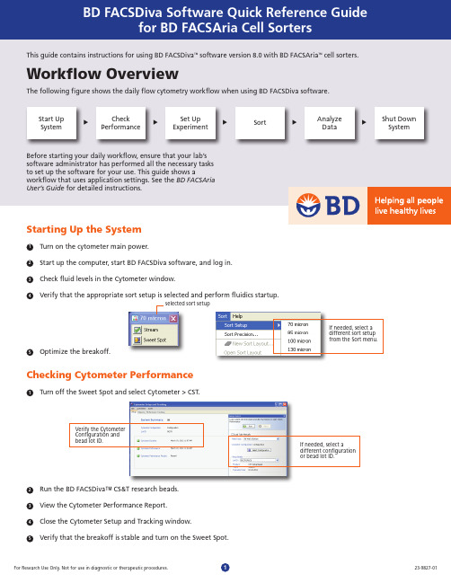
Workflow OverviewThe following figure shows the daily flow cytometry workflow when using BD FACSDiva software.Before starting your daily workflow, ensure that your lab’s software administrator has performed all the necessary tasks to set up the software for your use. This guide shows aworkflow that uses application settings. See the BD FACSAria User’s Guide for detailed instructions.Start Up SystemCheck PerformanceSet Up ExperimentSortAnalyze DataShut Down SystemtttttStarting Up the SystemTurn on the cytometer main power. Start up the computer, start BD FACSDiva software, and log in. Check fluid levels in the Cytometer window.Verify that the appropriate sort setup is selected and perform fluidics startup.Optimize the breakoff.Checking Cytometer PerformanceTurn off the Sweet Spot and select Cytometer > CST.Run the BD FACSDiva™ CS&T research beads. View the Cytometer Performance Report. Close the Cytometer Setup and Tracking window.Verify that the breakoff is stable and turn on the Sweet Spot.This guide contains instructions for using BD FACSDiva ™ software version 8.0 with BD FACSAria ™ cell sorters.Verify the CytometerConfiguration and bead lot ID.If needed, select adifferent configuration or bead lot ID.selected sort setupIf needed, select adifferent sort setup from the Sort menu.1234515432Setting Up the ExperimentCreate a new experiment and apply the Doublet Discrimination analysis template.Right-click in the Browser and select Application Settings > Apply.Select Experiment > Compensation Setup > Create Compensation Controls.Load the unstained control tube.Record data for the compensation control tubes.View the recorded data and gate the positive populations.Select an application setting.Click Overwrite if necessary.View data in the normalworksheets provided.Adjust the P1 gate,right-click, and select Apply to All Compensation Controls.Adjust the P2 gates to fit the positive populations.Verify that the FSC, SSC, and threshold settings are appropriate.1234567Select Experiment > Compensation Setup > Calculate Compensation.Record pre-sort data.Create sorting gates.Rename thecompensation setup.Use the Worksheet toolbar to create additional plots and gates.Format SSC-H vs SSC-W and FSC-H vs FSC-W plots to display All Events and adjust gates to exclude doublets.10Specify criteria under Acquistion Setup.Create gates for sorting particles of interest.89Remove the collection tubes.Set the drop delay using the Accudrop Drop Delay experiment template and BD FACS™ Accudrop beads.Click Start Run in the dialog and monitor the progress until complete.Open your sorting experiment and set up the Sort Layout.Adjust sliders as needed.Bring in theprovided experiment template.Adjust the flow rate until the threshold rate is appropriate for your nozzle size.Sort beads, then click Auto Delay.Make appropriateselections and entries.2345Stop the sort and save a copy of the sort report.Analyzing DataRecord post-sort data. Check the sort purity.Do one of the following to print or export the results:• Select File > Print to print the active worksheet. • Select File > Export to export selected elements.• Right-click a specimen or experiment and select Batch Analysis (using a global worksheet).Shutting Down the SystemPerform a fluidics shutdown or clean the flow cell. Perform external cleaning. Turn off the cytometer main power and shut down the computer.Specify where to save the PDF , XML, and exported statistics files.Select theoptions needed.7123123。
OB2283 Demo Board Manual(A)_天晖_130911
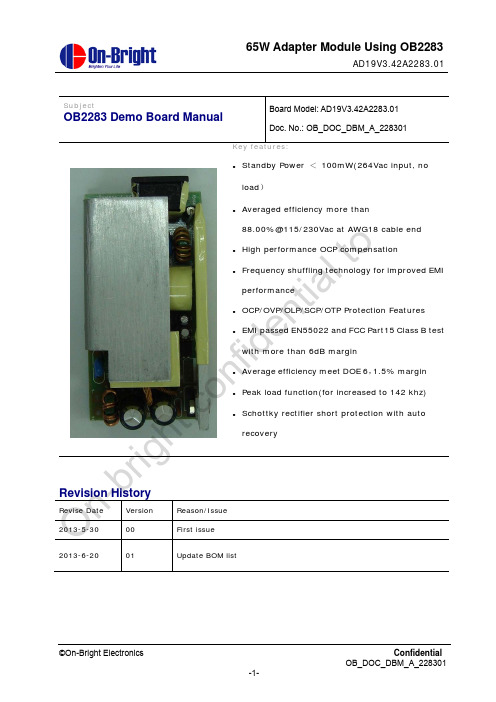
5 Thermal Test........................................................................................................................................ 20 6 Other important waveform ................................................................................................................. 20 6.1 CS, FB, Vdd & Vds waveform at no load/full load...................................................................... 20 6.2 Vds and Secondary diode waveform at full load, start/normal/output short ............................... 21 6.2.1 Vds and Secondary diode at full load, start/normal/output short ............................................ 21 6.2.2 Vds at full load, start waveform ............................................................................................... 21 6.2.3 Vds and Secondary diode at full load, normal waveform........................................................ 22 6.2.4 Vds and Secondary diode at full load, output short waveform................................................ 22
VIAVI Solutions ONA-800 FTTA OTDR 测试用户指南说明书

Quick CardOneAdvisor ONA-800FTTA OTDR, Cell Tower Construction and MaintenanceThis quick card explains how to connect to a fiber under test, configure Fiber to the Antenna (FTTA) OTDR test setups, run tests, and analyze results with a VIAVI ONA-800 equipped with a 4100 series OTDR. Equipment Requirements:• ONA-800 equipped with the following:o Fiber Optics Software Release V19.92 or greatero E4100 Series OTDR Moduleo Software options for FTTA OTDR andSmartLink Mapper (SLM) icon-based OTDR results• Fiber optic cleaning and inspection tools• 20-meter fiber optic patch cable (Launch Cable) with connectors that match the OTDR Port and Fiber Under Test (SC UPC, SC APC, LC UPC, etc.) • Optical Coupler to connect Launch Cable to BBU Jumper Cable or Trunk CableFigure 1: Equipment RequirementsThe following information is required to complete the procedure: • Type of Fiber (Multimode or Single Mode)• Type of Connectors (SC UPC, SC APC, LC UPC, etc.) • Tower architecture:o Is there a BBU jumper cable? o Is there an RRU jumper cable? • RRU and BBU/Base Station IDs • Fiber Code (1-Rx, 1-Tx, …, 24-Tx)Fiber Inspection Guidelines:• All fiber end-faces must be clean and pass an inspection test prior to connection.• Use the VIAVI P5000i or FiberChek Probe microscope to inspect both sides of every connection being used (SFP Port, bulkhead connectors, patch cables, etc.)Figure 2: Inspect Before You ConnectConnect to Fiber Under Test (FUT):All fibers and connectors should pass fiber inspection prior to connection, as described on page 1. The OTDR may be connected to the FUT as follows:Figure 3: Tower Architecture with BBU Jumper Figure 4: Tower Architecture, no BBU Jumper1.Inspect and clean the OTDR port on top of the test set.2.If the interface to the FUT is the BBU Jumper or Trunk Cable, connect the cable to an optical couplerwith the same connector type.3.Inspect and clean the FUT connected to the coupler or Optical Patch Panel (OPP).4.Inspect and clean fiber end face of the Launch Cable.5.Connect the Launch Cable to the OTDR port.6.Inspect and clean the other fiber end face of the Launch Cable.7.Connect the Launch Cable to the coupler or OPP leading to the RRU.Launch and Configure FTTA OTDR:Figure 5: Home Screen1.Press the Power button to start the test set.2.Tap to display the Home screen.3.Tap to display test selections.4.Tap the Fiber 1 selection to display OTDR module test selections. Note: TheModel number of your OTDR is displayed in the parenthesis.5.Tap to launch the FTTA OTDR test application.Figure 3: FTTA OTDR6.Tap the soft key to display the File Explorer.Figure 4: File Explorer7.Navigate to the ONA-800/disk/config/FTTA folder.8.Select FTTA_RRU_Maintenance.SM-OTDR for testing to an RRU at the far-end, orSelect FTTA_RRU_ConstrLoop.SM-OTDR for testing to a loopback at the far-end.9.Tap the and tap soft key to display FTTA OTDR Setup.Figure 5: Setup10.Configure Analysis settings as follows:•Set BBU Jumper to Yes if there is a BBU Jumper Cable between the Launch Cable and OVP;Set BBU Jumper to No if the Launch Cable is directly connected to the OVP.•Set RRU Jumper to Yes if there is a Junction Box/OVP at the top of the tower between the Trunk Cable and RRU; Set RRU Jumper to No if there is no Junction Box or no RRU Jumper.•Leave other settings at default values.11.Configure Link Description settings as follows:•Set Base Station ID to the Base Station or BBU Identifier.•Set RRU ID to the RRU Identifier or sector (Alpha, Beta, Gamma).•Set Fiber Code to the fiber number and polarity using the up and down arrows.•Set Change Fiber Nbr to Increment.•Set Distance Unit to feet or meter.Run Test:Press the icon to start the test. The OTDR will perform an auto-configuration, Connection Check, and Acquisition on each wavelength. If the Connection is Bad, repeat steps 1 through 7 on page 2, to ensurethe patch cable is clean and undamaged. Results will be auto-stored to the current directory.View Results:Result may be displayed in 3 different formats: SmartLink, Trace, or Table. The view is selected at the topof the display.Figure 6: View selection•SmartLink view:o In the upper display, the FUT is displayed as a series of icons representing events (end-of-fiber, launch cable, connector, etc.). Swipe left to display additional icons/events.o The center of the display shows summary results per wavelength. Acquisitions for which all events are acceptable are marked with a green check.o Tap on any icon to display event type and pass/fail status and to label each icon according to your tower architecture, in the lower display:▪BBU: Connection (coupler) between launch cable and BBU Jumper Cable▪BOT TWR: Optical Patch Panel at bottom of tower▪TOP TWR: Junction Box/Patch Panel at Top of tower▪RRU: End of RRU Jumper CableFigure 7: SmartLink ViewVIAVI SolutionsContact Us +1 844 GO VIAVI ) (+1 844 468 4284) To reach the VIAVI office nearest you,visit /contacts. © 2021 VIAVI Solutions Inc.Product specifications and descriptions in thisdocument are subject to change without notice.• Trace view :o Results for each wavelength are shown in different colors in the top section of the display. Each event iso Tap the icon to Auto-zoom the trace.o Tap 1 or 2 at the top of the display to toggle between results for the two wavelengths.Figure 8: Trace View• Table View: Each event on the FUT is displayed in tabular format.Figure 9: Table View。
AD838操作及设定指导手册课件
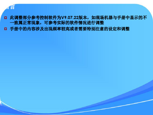
保证胶尾部变得光滑,在高速运动中不会飞溅 所有设定以达到点胶和装片速度可以匹配为佳
Dispenser parameter
推荐的参数设定如下
前言
此调整部分参考控制软件为V9.07.22版本,如现场机器与手册中显示的不 一致属正常现象,可参考实际的软件情况进行调整
手册中的内容涉及出现频率较高或者需要特别注意的设定和调整
Wafer table
Wafer table
Wafer table最常见的问题是无法自动打开或者关闭芯片扩张器,此部分 需进行硬件的调整和软件的检测
4.机器图像识别到的胶的大小为0.839 平方毫米, 此数值将成为之后检测点胶大小的依据 5.至此,Pre bond教读完成
Device change
6.点击Src Pre Bond菜单,进行Pre Bond 搜索, 得到一个点胶位置和target之间的差别的数据
7.提示点胶位置和点胶目标位置有位置差别, 点击Yes则下次点胶点在target位置附件,前提条件是 Src Pre Bond后Epoxy center 绿+需要在胶的中心附近, 否则则按No,不进行矫正 选取左右点胶器点出的胶的位置分别进行矫正
手工调整调整装片位置(粗略调整)
建议每班交接后在首次生产时检查此功能是否正常
Miss die sensor setting
Miss die sensor
Miss die感应器调整不当会引起漏吸芯片不报警,或者芯片被带回不报警 等情况
1.首先调整上下 键使下排绿灯停留在数字1下面 2.打开吸嘴真空电磁阀开关,可以看见表上的数值显示(一般大于60),
新一代8位微控制器EFM8系列产品说明书
新闻稿Silicon Labs推出新一代8位微控制器迎接物联网时代-最新节能型EFM8 MCU系列产品为成本和空间受限的设计提供无与伦比的简便性、外设集成和性能-中国,北京-2015年3月2日-物联网(IoT)领域节能型微控制器解决方案供应商Silicon Labs(芯科科技有限公司,NASDAQ:SLAB)今日宣布推出新一代8位MCU系列产品,该产品旨在满足当今超低功耗、小尺寸的IoT应用。
Silicon Labs的新型EFM8 MCU系列产品包括三种类型高集成度、外设丰富的MCU,这些MCU特别针对高性价比、超低功耗电容式触摸控制和精简USB连接而进行了优化。
EFM8 MCU为嵌入式开发人员所能想到的所有8位应用提供了业内领先的简便性、能效、性能和成本节省的综合优势,应用涵盖家居和楼宇自动化、可穿戴、消费类电子、玩具、电机控制和工业IoT等。
HIS Technology公司MCU首席分析师Tom Hackenberg表示,“为了在可预见的未来保持MCU市场的蓬勃发展,领先的MCU供应商持续不断的推动8位解决方案在能耗和集成特性上的发展。
根据IHS的预测,8位市场规模在2015年将达到70亿美元,2018年将增长到78亿美元,市场份额继续超过每年MCU市场营收的三分之一以上。
这种稳定的增长归功于市场对于0.5美元以下MCU在价格、极小封装、超低功耗、较低软件开销和简化设计的需求,这些也是IoT设备的先决条件。
Silicon Labs所设计的新型EFM8系列产品在这些关键应用领域中都具有最佳的特性和功能。
EFM8 MCU系列产品完全满足IoT开发人员的需求,提供无与伦比的特性和性能等综合优势,这包括高速流水线8051内核、超低功耗、精度模拟、增强的通信外设、集成的振荡器、小尺寸封装,以及能够提供灵活的数字和模拟复用、简化印刷电路板(PCB)设计和I/O引脚路由的先进Crossbar架构。
新型的EFM8 Bee系列产品包括三类MCU产品,这些产品为满足特定开发人员的需求和应用而进行了优化。
TA838中文
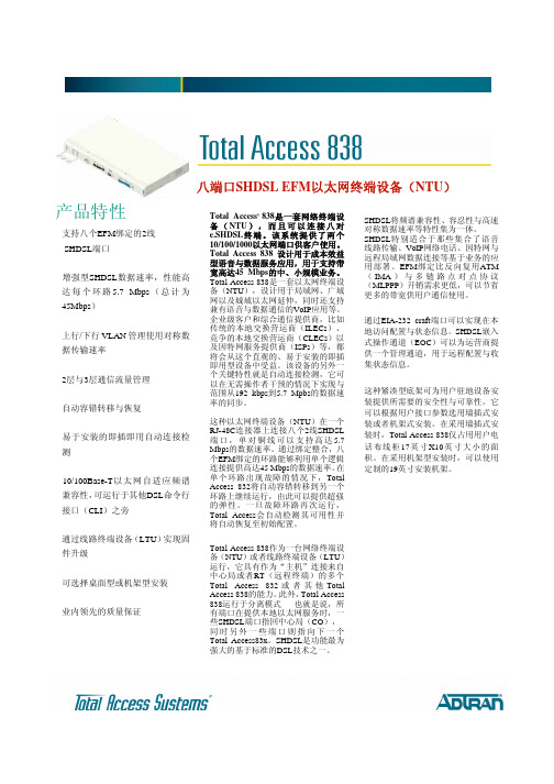
产品特性■支持八个EFM 绑定的2线SHDSL 端口■增强型SHDSL 数据速率,性能高达每个环路5.7 Mbps (总计为45Mbps )■上行/下行VLAN 管理使用对称数据传输速率■2层与3层通信流量管理■自动容错转移与恢复■易于安装的即插即用自动连接检测■10/100Base-T 以太网自适应频谱兼容性,可运行于其他DSL 命令行接口(CLI )之旁■通过线路终端设备(LTU )实现固件升级■可选择桌面型或机架型安装■业内领先的质量保证Total Access ®838是一套网络终端设备(NTU ),而且可以连接八对e.SHDSL 终端。
该系统提供了两个10/100/1000以太网端口供客户使用。
Total Access 838 设计用于成本效益型语音与数据服务应用,用于支持带宽高达45 Mbps 的中、小规模业务。
Total Access 838是一套以太网终端设备(NTU ),设计用于局域网、广域网以及城域以太网延伸,同时还支持兼有语音与数据通信的VoIP 应用等。
企业级客户和综合通信提供商,比如传统的本地交换营运商(ILECs )、竞争的本地交换营运商(CLECs )以及因特网服务提供商(ISPs )等,都将会从这个直观的、易于安装的即插即用型设备中受益。
该设备的另外一个关键特性就是自动连接检测,它可以在无需操作者干预的情况下实现与范围从192 kbps 到5.7 Mpbs 的数据速率的同步。
这种以太网终端设备(NTU )在一个 RJ-48C 连接器上连接八个2线SHDSL 端口,单对铜线可以支持高达5.7 Mbps 的数据速率。
通过绑定整合,八个EFM 绑定的环路能够利用单个逻辑连接提供高达45 Mbps 的数据速率。
在单个环路出现故障的情况下,Total Access 832将自动容错转移到另一个环路上继续运行,由此可以提供超强 的弹性。
一旦故障环路再次运行,Total Access 会自动检测其可用性并将自动恢复至初始配置。
安捷伦RNA 6000 Pico试剂盒说明书
Agilent RNA 6000 Pico Kit, Part Number 5067-1513*************(24小时)化学品安全技术说明书GHS product identifier 应急咨询电话(带值班时间)::供应商/ 制造商:安捷伦科技贸易(上海)有限公司中国(上海)外高桥自由贸易试验区英伦路412号(邮编:200131)电话号码: 800-820-3278传真号码: 0086 (21) 5048 2818Agilent RNA 6000 Pico Kit, Part Number 5067-1513化学品的推荐用途和限制用途安全技术说明书根据 GB/ T 16483-2008 和 GB/ T 17519-2013GHS化学品标识:安捷伦RNA 6000 皮克试剂盒,部件号 5067-1513推荐用途限制用途RNA Pico Conditioning Solution1 x 0.3 ml -RNA Pico Gel Matrix2 x 1.2 ml -RNA Pico Dye Concentrate1 x 0.035 ml -RNA Pico Marker4 x 0.6 ml -RNA Pico Ladder1 x 0.01 ml::物质或混合物的分类根据 GB13690-2009 和 GB30000-2013紧急情况概述液体。
液体。
RNA Pico Dye Concentrate 液体。
RNA Pico Marker 液体。
RNA Pico Ladder 液体。
无资料。
无资料。
RNA Pico Dye Concentrate 蓝色。
RNA Pico Marker 无资料。
RNA Pico Ladder 无资料。
无资料。
无资料。
RNA Pico Dye Concentrate 无资料。
RNA Pico Marker 无资料。
RNA Pico Ladder 无资料。
没有明显的已知作用或严重危险。
IQRF Tech TR-76D RF Transceiver Module 数据手册说明书
TR-76DRF Transceiver Module SeriesData SheetBlock diagramKey features• Operating system (upgradeable at the user), easy to use • DPA framework for Data controlled approach (formerly DCTR) • GFSK modulation• Selectable RF band 868 / 916 MHz, multiple channel • RF output power 10 mW• MCU with extended resources, user interrupt capability • Extra low power consumption, power management modes • SPI interface supported by OS in background • Serial EEPROM 256 Kb • PWM output• Programmable HW timer • Battery monitoring• 18 pins, 11 I/O pins, 1 input only pin• A/D converter (4 channels), D/A converter, analog comparator • Options: on-board antenna or soldering antenna pad-hole• Stamp-hole pads, SMT mounting, compatible with SIM card connector without metallic holder (KON-SIM-02) • Shielding canApplications• Bidirectional RF communication• Point-to-point or network wireless connectivity • Telemetry, AMR (automatic meter reading) • WSN (wireless sensor network) • Building automation • Street lighting control• Wireless monitoring, control and regulation • Remote data acquisition• RF connectivity in many other fields • Also for municipal and indoor areas • Internet of ThingsElectrical specificationsTypical values unless otherwise statedSupply voltage (V CC ) 13.0 V min., 3.4 V max., stabilizedOperating temperature 2-40 °C to +85 °CSupply currentDeep sleep mode (OS v4.00 or higher only) 56 nA (all peripherals disabled4, RF IC in Standby mode) Sleep mode610 nA (all peripherals disabled 4, RF IC in Sleep mode)Run modeRF sleep 1.6 mA RF ready3.0 mARX modeSTD 11.8 mA LP 5 250 µA XLP 5 16.3 µATX mode8.3 mA – 25 mA (according to RF output power)RF band 868 MHz or 916 MHz (software configurable)RF channelsSee IQRF OS User’s guide, Appendix Channel maps RF data modulationGFSK (Gaussian Frequency Shift Keying) RF data transmission bit rate 619.8 kb/sRF receiver category 1.5 (according to ETSI EN 300 220-1 V3.1.1)RF sensitivity 7-101 dBm (STD RX mode, checkRF(0)). See Diagram 4.RF output power (TR-76D) 7Up to 10 dBm (for 50 Ω load), programmable in 8 levels (0 – 7).Effective radiated power (TR-76DA) Up to 6.5 dBm 3A , 11 dBm 3B (868 MHz band), 2.0 to 6.5 dBm 3A (916 MHz band).See Diagrams 2A, 2B .RF interface (TR-76D)Single-ended, output impedance 50 ΩAntenna (TR-76DA)PCB meander line, linear polarization, omnidirectional. See Diagram 1.RF range (TR-76DA)500 m 3A , 1100 m 3BInput voltage on Q4 to Q15 pins0 V to VCCA/D converter10 bit, 4 inputs. Refer to MCU datasheet.Size (L x W x H) 15.2 mm x 14.9 mm x 3.3 mm (TR-76D)23.3 mm x 14.9 mm x 3.3 mm (TR-76DA)Note 1: RF power and other parameters depend on the supply voltage. Refer to datasheets of MCU and RF IC used. Test yourapplication with respect to required supply voltage range.Note 2: RF range may change with lower temperature. Frost, condensation or humidity over 85% may disable module functionality.Module suitability should be tested in the final application at real conditions before volume use.Note 3: Arrangement: Two TR-76DA transceivers plugged in DK-EVAL-04A kits, vertically, 1.6 m above the ground, in free space,bidirectional communication.3A: TR-76DA transceivers plugged in DK-EVAL-04A kits through the KON-TR-01 adapters.3B: TR-76DA transceivers plugged in DK-EVAL-04A kits through the RNG-EXT-01 adapters.Test software: E09-LINK example (STD mode, setRFpower(7), checkRF(0)), bit rate 19.8 kb/s.Note 4: Additional current is consumed when a peripheral (e.g. watchdog, Brown-out detection etc.) is enabled. Note 5: Depends on interferences.Note 6: Several RF bit rates different from 19.8 kb/s will be available in future IQRF OS versions. Note 7: RF circuitry and RF balun included, built-in PCB antenna not included.Absolute maximum ratingsSupply voltage (V CC ) 3.9 VVoltage on Q4 to Q15 pins (configured as inputs) vs. GND -0.3 V to (V CC + 0.3 V) Storage temperature -40 °C to +85 °C Ambient temperature under bias-40 °C to +85 °CSee the application note AN015 - IQRF HW design for TR-7xD transceivers .Simplified schematicBasic componentsFor more information refer to datasheets of ICs used.Pin Name DescriptionQ1 1GND GroundQ2, C4GND Ground Top viewQ3, C3V CC Power supply voltageQ4IO / TX / PWMRC6General I/O pinTX UART TXCCP3PWM outputQ5IO / RXRC7General I/O pinRX UART RXQ6, C6IO / SCK / SCLRC3General I/O pinSCK SPI clock inputSCL I2C clockQ7 2, C7IO / SDI / SDARC4General I/O pinSDI SPI dataSDA I2C dataQ8 2, C8IO / SDORC5General I/O pinSDO SPI data outQ9, C5IO / ADC / -SS / COUT Bottom view RA5General I/O pinAN4Analog A/D input-SS SPI Slave selectC2OUT Comparator outputQ10 3IO / LEDGRB7 General I/O pin, programmable pull-upInterrupt/Wake-up on change (IOC)LED1 LEDG supported by OSQ11 3IO / ADC / LEDRRA2General I/O pinAN2Analog A/D inputLED2LEDR supported by OSDACOUT D/A converter outputQ12IO / ADCRB4General I/O pin, with programmable pull-upInterrupt/Wake-up on change (IOC)RFPGM / (X)LP mode terminationAN11Analog A/D inputQ13INRE3General input only pinQ14, C1IO / ADC / C-INRA0General I/O pinAN0Analog A/D inputC12IN0Comparator –inputQ15, C2IORC2General I/O pinQ16–Do not use, leave unconnectedQ17 1GND GroundQ18 1ANT AntennaP1–P5For manufacturer onlyNote 1: Not implemented for TR-76DA.Note 2:Pin Q8 is used as output and pin Q7 as input during the initial approximately 200 ms boot-up (after power supply rising-up) to detect a possible request to enter the programming mode (PGM - wired upload via SPI). After reset, the OS generates adeterminate sequence on the Q8 pin. If this sequence is copied to the Q7, the OS jumps to the PGM bootloader. (The PGMmode is indicated by short red LED flashing every 2 s.)This must be taken into account to avoid collisions with application circuitry connected to these pins.The Q7 pin must not be interconnected to Q8 or left unconnected or without a defined level on its input. Thislevel must be arranged by application hardware. If the application circuitry ensures no such level, a pull-down resistor on Q7 pin must be used otherwise a cross-talk between Q8 and Q7 may cause anunintentional switching to PGM.Note 3: This pin is affected by IQRF OS (and possibly DPA) LED functions and system LED indication.There are no on-board protection series resistors on I/O pins. It is recommended to use 200 Ω series resistors on each pin. See the application note AN015 - IQRF HW design for TR-7xD transceivers.Recommended circuit for developmentFor development, it is recommended to implement the following arrangement:•Decoupling capacitor on V CC to filter the supply voltage. The type and the value should be selected with respect to general rules observed in electronic design, according to given application hardware and power source.•Serial protective resistors on each I/O pin used.•Both system LEDs (LEDR and LEDG) for IQRF OS and DPA status indication and for possible user indication. When the Q10 and Q11 pins are used as user I/Os, it must be taken into account that these pins can be affected by IQRF OS or DPA.•Pin Q12 configured as an input with the internal pull-up resistor and equipped with a pushbutton connected to the ground.Then pressing the button can generate an interrupt on pin change, wake-up the transceiver from sleep, terminate RFPGM mode, initiate bonding etc.•Pull-down resistor on pin Q7 recommended to avoid unintentional switching to PGM mode due to SDO - SDI cross-talk during TR boot.•SPI interface for wired upload of application code into the transceiver using an IQRF programmer, e.g CK-USB-04A.RF rangeRF range strongly depends on the following design aspects:•Hardware:•Construction of the devices (especially TR location within the device, PCB layout, ground planes, conductive areas and bulk objects such as metallic parts and batteries in the nearest surroundings, with respect to possible reflections and counterpoise effect). To achieve an efficient range and reliable connectivity, no parts impacting the range must be placed close to the built-in meander antenna. Even non-conductive parts including a mainboard PCB under the antenna can significantly impact the range.•Physical arrangement of devices (especially mutual orientations of antennas with respect to polarizations and radiation patterns)•Application software:•RF output power is selectable from 8 levels•To increase immunity to RF noise, incoming RF signal can be filtered according to signal strength.Refer to IQRF OS Reference guide, function checkRF and Application note AN014 RF range optimizing at TR-7xDx transceivers.Diagram 1: TR-7xDA RF output power [in dBm] vs. antenna orientation (radiation patterns).Examples of the correct and incorrect arrangement of TR-7xDA pairs:Correct Correct Incorrect Incorrect IncorrectWrong radiation angle Mismatched polarization Wrong radiation angleMismatched polarizationDiagram 2A: Effective radiated power (ERP) vs. level in the setRFpower(level) function. TR-76D(A), 868 MHz band, channels 0 to 67. Refer to IQRF OS Reference guide.Diagram 2B: Effective radiated power (ERP) vs. level in the setRFpower(level) function. TR-76D(A), 916 MHz band. Refer to IQRF OS Reference guide.Diagram 2C: Relative RF range vs. level in the setRFpower(level) function. TR-76D(A), 868 MHz and 916 MHz bands. Refer to IQRF OS Reference guide.Diagram 3A: Relative effective radiated power (ERP) vs. channel, with respect to channel 52 (100 %). TR-76D(A), 868 MHz band.Diagram 3B: Relative effective radiated power (ERP) vs. channel, with respect to channel 104 (100%). TR-76DA, 916 MHz band.Diagram 4: Relative RF range vs. level in the checkRF(level) function in STD, LP and XLP RX modes. Refer to IQRF OS Reference guide.Diagram 5: Relative RF range vs. antenna height above the ground. TR-76DA, 868 MHz and 916 MHz bands.Mechanical drawingsTR-76DTR-76DATop view. Units: mm.Hardware revision•TR-76DA v1.05 Minor improvements to optimize production.•TR-76D(A) v1.04 Minor improvements to optimize production.•TR-76D(A) v1.02 Minor improvements to optimize production. TR-76DA also for 916 MHz band.•TR-76D(A) v1.01 Minor improvements to optimize production. TR-76DA for 868 MHz band only.•TR-76D(A) v1.00 First standard release. TR-76DA for 868 MHz band only.ApplicationSee IQRF video tutorial set on /videos.See the application noteAN015 - IQRF HW design for TR-7xD transceivers .AssemblyFor proper mounting of surface mount TR modules and avoiding damage during solder reflow assembly, refer to the reflow profile and other details in the Application note AN015 – IQRF HW design , chapter SMT mounting .It is not allowed to connect wires to pads C1 to C8 and P1 to P5 by soldering.Recommended PCB layoutTR-76D TR-76DAPadsTop view. Units: mm.Restricted areas for wires on top sideThese patterns are for reference purposes only. Consult your producer to ensure that its manufacturing guidelines are met.SealingIn case of sealing or protecting TR modules against a harsh environment by coating, encapsulating or potting using a lacquer, gel or other filling matter, refer to the Application note AN015 – IQRF HW design for TR-7xD transceivers, chapter Sealing. Operating systemSee IQRF OS User's guide and IQRF OS Reference guide.DPA frameworkSee DPA Framework technical guide.Application softwareSee IQRF Quick start guide and IQRF application examples.Programming (upload)There are the following possibilities to upload an application program in TR-76Dx modules:•Wired upload with TR-76Dx plugged via the SIM connector in the CK-USB-04A programmer.•For TR-76Dx modules populated in an application:•Wired upload•Using the CK-USB-04A programmer. See the CK-USB-04A User's guide.•Using the CK-USB-04 programmer and the KON-TR-01P adapter. See the KON-TR-01P User's guide.•Completely arranged by user application. See the IQRF SPI Technical guide, chapter Programming mode.•Wireless upload: See the IQRF OS User's guide, Appendix RFPGM – RF programming TM.Product informationOrdering codesT R-76D AAntenna optionsnil - soldering pad-hole (no antenna, no U.FL connector)A - PCB antennaTransceiver series. TR/DCTR are not differentiated from IQRF OS v4.02D.TR-76D TR-76DADocument history•200525 References to application note AN015 – IQRF HW design for TR-7xD transceivers added.•191209 Note 2 in Pin description table extended. Paragraph Programming (upload) in chapter Application slightly extended. Chapters Assembly and Sealing relocated into Application note AN015 – IQRF HW design,chapters SMT mounting and Sealing.•191010 Supply current in TX mode and Note 3A in Electrical specifications modified. Legend added to chapter Recommended PCB layout. Updated for TR-76DA HW version 1.05.•180627 Diagram 2C added. Decoupling capacitor added to Recommended circuit for development.•180130 Block diagram revised. RF parameters in chapter Electrical specifications revised. HW revisions updated.Chapter RF range extended. Directives in Quality management updated.•171108 Note 3 in chapter Electrical specification revised. The legend at Diagrams 2A, 2B, 3A and 3B slightly precised.•170823 A bug in Recommended PCB layout fixed. Updated for IQRF OS v4.02D.•170810 V CC reduced to 3.9 V in chapter Absolute maximum ratings. Diagram 4, Mechanical drawings and Recommended PCB layout updated. Updated for TR/DCTR fusion from IQRF OS v4.02D. Some minorimprovements.•170322 Diagrams 3A and 3B added. Preliminary.•170314 Updated for HW v1.02 and IQRF OS v4.00 (preliminary). Electrical specification revised. Chapter Sealing added. Chapter Recommended circuit for development slightly extended. Variances in mechanicaldrawings slightly precised. Some minor improvements.•160304 Pin Q12 description slightly extended.•160219 More detailed RF range specification. Q7 and Q8 pin description extended.•160118 Note 10 added to pin description table. Chapter Recommended circuit for development added.A bug in Key features, antenna options fixed.•151005 ETSI directives updated. Preliminary.•151001 First release. Preliminary.Sales and ServiceCorporate officeIQRF Tech s.r.o., Prumyslova 1275, 506 01 Jicin, Czech Republic, EUTel: +420 493 538 125, Fax: +420 493 538 126, www.iqrf.techE-mail (commercial matters): **************Technology and developmentE-mail (technical matters): ****************Partners and distribution/partnersQuality managementISO 9001 : 2009 certifiedComplies with ETSI directives EN 301 489-1 V1.9.2:2011, EN 301 489-3 V1.6.1:2013,EN 300 220-1 V3.1.1:2017, EN 300 220-2 V3.2.0:2017 and ERC Recommendation70-03 (2017) and VO-R/10/05.2014-3.Complies with directives 2011/65/EU (RoHS) and 2012/19/EU (WEEE).TrademarksThe IQRF name and logo are registered trademarks of IQRF Tech s.r.o.PIC, SPI, Microchip and all other trademarks mentioned herein are a property of their respective owners.LegalAll information contained in this publication is intended through suggestion only and may be superseded by updates without prior notice. No representation or warranty is given and no liability is assumed by IQRF Tech s.r.o. with respect to the accuracy or use of such information.Without written permission, it is not allowed to copy or reproduce this information, even partially.No licenses are conveyed, implicitly or otherwise, under any intellectual property rights.The IQRF® products utilize several patents (CZ, EU, US).On-line support: ****************。
美国博士科技(Amphenol)817型号光电转换器说明书
Dimensions: [mm]2112Scale - 3:1Würth Elektronik eiSos GmbH & Co. KG EMC & Inductive Solutions Max-Eyth-Str. 174638 Waldenburg Germany140817141010Würth Elektronik eiSos GmbH & Co. KGEMC & Inductive Solutions140817141010 Max-Eyth-Str. 174638 WaldenburgGermanyTotal Power Dissipation vs. Ambient Temperature:20406080100120140160-55-35-15525456585105125IR-diode -I F(mA)Ambient Temperature (°C)Phototransistor-PO(mW)CollectorPowerDissipation(mW)ForwardCurrent(mA)Collector Dark Current vs. Ambient Temperature:11010010001000025456585105125CollectorDarkCurrent(nA)Ambient Temperature (°C)V CE= 20VV CE= 10VNote: measured with Bin BWürth Elektronik eiSos GmbH & Co. KGEMC & Inductive SolutionsMax-Eyth-Str. 174638 WaldenburgGermanyCHECKED REVISION DATE (YYYY-MM-DD)GENERAL TOLERANCE PROJECTIONMETHODSaVo001.0052023-08-22DIN ISO 2768-1mDESCRIPTIONWL-OCPT OptocouplerPhototransistor ORDER CODE140817141010SIZE/TYPE BUSINESS UNIT STATUS PAGEAbsolute CTR vs. Ambient Temperature50100150200250300-60-40-20020406080100120AbsoluteCTRAmbient Temperature (°C)V CE= 5VV CE= 0,4VTestcondition: I F=5mA, T A=25°C, Bin BRelative CTR vs. Ambient Temperature:0,40,60,811,21,4-60-40-20020406080100120RelativeCTRAmbient Temperature (°C)V CE= 5VV CE= 0,4VTestcondition: I F=5mA, Normalized to T A=25°C, Bin BWürth Elektronik eiSos GmbH & Co. KGEMC & Inductive SolutionsMax-Eyth-Str. 174638 WaldenburgGermanyCHECKED REVISION DATE (YYYY-MM-DD)GENERAL TOLERANCE PROJECTIONMETHODSaVo001.0052023-08-22DIN ISO 2768-1mDESCRIPTIONWL-OCPT OptocouplerPhototransistor ORDER CODE140817141010SIZE/TYPE BUSINESS UNIT STATUS PAGEWürth Elektronik eiSos GmbH & Co. KGEMC & Inductive Solutions140817141010 Max-Eyth-Str. 174638 WaldenburgGermanyWürth Elektronik eiSos GmbH & Co. KGEMC & Inductive Solutions140817141010 Max-Eyth-Str. 174638 WaldenburgGermany050100150200250300350400450A b s o l u t e C T R (%)Testcondition T A Würth Elektronik eiSos GmbH & Co. KG EMC & Inductive Solutions Max-Eyth-Str. 174638 Waldenburg Germany140817141010050100150200250300A b s o l u t e C T R (%)Testcondition T A Würth Elektronik eiSos GmbH & Co. KG EMC & Inductive Solutions Max-Eyth-Str. 174638 Waldenburg Germany1408171410100102030R e s p o n s e T i m e (µs )Testcondition I C Würth Elektronik eiSos GmbH & Co. KG EMC & Inductive Solutions Max-Eyth-Str. 174638 Waldenburg Germany140817141010Würth Elektronik eiSos GmbH & Co. KGEMC & Inductive Solutions140817141010 Max-Eyth-Str. 174638 WaldenburgGermanyWürth Elektronik eiSos GmbH & Co. KGEMC & Inductive Solutions140817141010 Max-Eyth-Str. 174638 WaldenburgGermanyT e m p e r a t u r eT T T Würth Elektronik eiSos GmbH & Co. KG EMC & Inductive Solutions Max-Eyth-Str. 174638 Waldenburg Germany140817141010Cautions and Warnings:The following conditions apply to all goods within the product series of Optoelectronic Components of Würth Elektronik eiSos GmbH & Co. KG:General:•This optoelectronic component is designed and manufactured for use in general electronic equipment.•Würth Elektronik must be asked for written approval (following the PPAP procedure) before incorporating the components into any equipment in fields such as military, aerospace, aviation, nuclear control, submarine, transportation (automotive control, train control,ship control), transportation signal, disaster prevention, medical, public information network, etc. where higher safety and reliability are especially required and/or if there is the possibility of direct damage or human injury.•Optoelectronic components that will be used in safety-critical or high-reliability applications, should be pre-evaluated by the customer. •The optoelectronic component is designed and manufactured to be used within the datasheet specified values. If the usage and operation conditions specified in the datasheet are not met, the wire insulation may be damaged or dissolved. •Do not drop or impact the components, the component may be damaged•Würth Elektronik products are qualified according to international standards, which are listed in each product reliability report. Würth Elektronik does not warrant any customer qualified product characteristics beyond Würth Elektroniks’ specifications, for its validity and sustainability over time.•The responsibility for the applicability of the customer specific products and use in a particular customer design is always within the authority of the customer. All technical specifications for standard products also apply to customer specific products.•Unless Würth Elektroik has given its express consent, the customer is under no circumstances entitled to reverse engineer, disassemble or otherwise attempt to extract knowledge or design information from the optoelectronic component.Product specific:Soldering:•The solder profile must comply with the technical product specifications. All other profiles will void the warranty. •All other soldering methods are at the customers’ own risk•The soldering pad pattern shown above is a general recommendation for the easy assembly of optoelectronic components. If a high degree of precision is required for the selected application (i.e. high density assembly), the customer must ensure that the soldering pad pattern is optimized accordingly.Cleaning and Washing:•Washing agents used during the production to clean the customer application might damage or change the characteristics of the optoelectronic component body, marking or plating. Washing agents may have a negative effect on the long-term functionality of the product.• Using a brush during the cleaning process may break the optoelectronic component body. Therefore, we do not recommend using a brush during the PCB cleaning process.Potting:•If the product is potted in the customer application, the potting material might shrink or expand during and after hardening. Shrinking could lead to an incomplete seal, allowing contaminants into the optoelectronic component body, pins or termination. Expansion could damage the components. We recommend a manual inspection after potting to avoid these effects.Storage Conditions:• A storage of Würth Elektronik products for longer than 12 months is not recommended. Within other effects, the terminals may suffer degradation, resulting in bad solderability. Therefore, all products shall be used within the period of 12 months based on the day of shipment.•Do not expose the optoelectronic component to direct sunlight.•The storage conditions in the original packaging are defined according to DIN EN 61760-2.•For a moisture sensitive component, the storage condition in the original packaging is defined according to IPC/JEDEC-J-STD-033. It is also recommended to return the optoelectronic component to the original moisture proof bag and reseal the moisture proof bag again. •The storage conditions stated in the original packaging apply to the storage time and not to the transportation time of the components.Packaging:•The packaging specifications apply only to purchase orders comprising whole packaging units. If the ordered quantity exceeds or is lower than the specified packaging unit, packaging in accordance with the packaging specifications cannot be ensured.Handling:•Violation of the technical product specifications such as exceeding the nominal rated current, will void the warranty. •The product design may influence the automatic optical inspection.•Certain optoelectronic component surfaces consist of soft material. Pressure on the top surface has to be handled carefully to prevent negative influence to the function and reliability of the optoelectronic components.•ESD prevention methods need to be applied for manual handling and processing by machinery. •Resistors for protection are obligatory.•In addition to optoelectronic components testing, products incorporating these devices have to comply with the safety precautions given in IEC 60825-1, IEC 62471 and IEC 62778.Technical specification:•The typical and/or calculated values and graphics of technical parameters can only reflect statistical figures. The actual parameters ofeach single product, may differ from the typical and/or calculated values or the typical characteristic line.Würth Elektronik eiSos GmbH & Co. KG EMC & Inductive Solutions Max-Eyth-Str. 174638 Waldenburg GermanyCHECKED REVISION DATE (YYYY-MM-DD)GENERAL TOLERANCEPROJECTION METHODSaVo001.0052023-08-22DIN ISO 2768-1mDESCRIPTIONWL-OCPT Optocoupler PhototransistorORDER CODE140817141010SIZE/TYPEBUSINESS UNITSTATUSPAGE•In the characteristics curves, all values given in dotted lines may show a higher deviation than the paramters mentioned above. •On each reel, only one bin is sorted and taped. The bin is defined on the current transfer ratio.•In order to ensure highest availability, the reel binning of standard deliveries can vary. A single bin cannot be ordered. Please contact us in advance, if you need a particular bin sorting before placing your order.•These cautions and warnings comply with the state of the scientific and technical knowledge and are believed to be accurate and reliable. However, no responsibility is assumed for inaccuracies or incompleteness.The customer has the sole responsibility to ensure that he uses the latest version of this datasheet, which is available on Würth Elektronik’s homepage. Unless otherwise agreed in writing (i.e. customer specific specification), changes to the content of this datasheet may occurwithout notice, provided that the changes do not have a significant effect on the usability of the optoelectronic components.Würth Elektronik eiSos GmbH & Co. KG EMC & Inductive Solutions Max-Eyth-Str. 174638 Waldenburg GermanyCHECKED REVISION DATE (YYYY-MM-DD)GENERAL TOLERANCEPROJECTION METHODSaVo001.0052023-08-22DIN ISO 2768-1mDESCRIPTIONWL-OCPT Optocoupler PhototransistorORDER CODE140817141010SIZE/TYPEBUSINESS UNITSTATUSPAGEImportant NotesThe following conditions apply to all goods within the product range of Würth Elektronik eiSos GmbH & Co. KG:1. General Customer ResponsibilitySome goods within the product range of Würth Elektronik eiSos GmbH & Co. KG contain statements regarding general suitability for certain application areas. These statements about suitability are based on our knowledge and experience of typical requirements concerning the areas, serve as general guidance and cannot be estimated as binding statements about the suitability for a customer application. The responsibility for the applicability and use in a particular customer design is always solely within the authority of the customer. Due to this fact it is up to the customer to evaluate, where appropriate to investigate and decide whether the device with the specific product characteristics described in the product specification is valid and suitable for the respective customer application or not.2. Customer Responsibility related to Specific, in particular Safety-Relevant ApplicationsIt has to be clearly pointed out that the possibility of a malfunction of electronic components or failure before the end of the usual lifetime cannot be completely eliminated in the current state of the art, even if the products are operated within the range of the specifications.In certain customer applications requiring a very high level of safety and especially in customer applications in which the malfunction or failure of an electronic component could endanger human life or health it must be ensured by most advanced technological aid of suitable design of the customer application that no injury or damage is caused to third parties in the event of malfunction or failure of an electronic component. Therefore, customer is cautioned to verify that data sheets are current before placing orders. The current data sheets can be downloaded at .3. Best Care and AttentionAny product-specific notes, cautions and warnings must be strictly observed. Any disregard will result in the loss of warranty.4. Customer Support for Product SpecificationsSome products within the product range may contain substances which are subject to restrictions in certain jurisdictions in order to serve specific technical requirements. Necessary information is available on request. In this case the field sales engineer or the internal sales person in charge should be contacted who will be happy to support in this matter.5. Product R&DDue to constant product improvement product specifications may change from time to time. As a standard reporting procedure of the Product Change Notification (PCN) according to the JEDEC-Standard inform about minor and major changes. In case of further queries regarding the PCN, the field sales engineer or the internal sales person in charge should be contacted. The basic responsibility of the customer as per Section 1 and 2 remains unaffected.6. Product Life CycleDue to technical progress and economical evaluation we also reserve the right to discontinue production and delivery of products. As a standard reporting procedure of the Product Termination Notification (PTN) according to the JEDEC-Standard we will inform at an early stage about inevitable product discontinuance. According to this we cannot guarantee that all products within our product range will always be available. Therefore it needs to be verified with the field sales engineer or the internal sales person in charge about the current product availability expectancy before or when the product for application design-in disposal is considered. The approach named above does not apply in the case of individual agreements deviating from the foregoing for customer-specific products.7. Property RightsAll the rights for contractual products produced by Würth Elektronik eiSos GmbH & Co. KG on the basis of ideas, development contracts as well as models or templates that are subject to copyright, patent or commercial protection supplied to the customer will remain with Würth Elektronik eiSos GmbH & Co. KG. Würth Elektronik eiSos GmbH & Co. KG does not warrant or represent that any license, either expressed or implied, is granted under any patent right, copyright, mask work right, or other intellectual property right relating to any combination, application, or process in which Würth Elektronik eiSos GmbH & Co. KG components or services are used.8. General Terms and ConditionsUnless otherwise agreed in individual contracts, all orders are subject to the current version of the “General Terms and Conditions of Würth Elektronik eiSos Group”, last version available at .Würth Elektronik eiSos GmbH & Co. KGEMC & Inductive SolutionsMax-Eyth-Str. 174638 WaldenburgGermanyCHECKED REVISION DATE (YYYY-MM-DD)GENERAL TOLERANCE PROJECTIONMETHODSaVo001.0052023-08-22DIN ISO 2768-1mDESCRIPTIONWL-OCPT OptocouplerPhototransistor ORDER CODE140817141010SIZE/TYPE BUSINESS UNIT STATUS PAGE。
ft838nbi 原理
ft838nbi 原理FT838NBI是一个假设性的设备或模块,目前在公开的技术资料中,并没有找到与之直接相关的详细信息。
然而,根据常见的技术命名规则和工业控制领域的一些背景知识,我们可以尝试构建一个关于“FT838NBI”可能涉及的原理概述。
鉴于“NBI”通常指代不同领域的特定技术组件(如核聚变中的中性束注入、工业自动化中的节点总线接口等),这里我们推测FT838NBI可能是一种新型的工业自动化或通信接口模块。
假设FT838NBI为一种工业自动化接口模块:FT838NBI可能是一款由某制造商设计开发的高级节点总线接口模块,用于工业自动化控制系统中实现设备间的高效数据传输与交互。
它可能遵循诸如基金会现场总线(Fieldbus Foundation)或PROFINET等现代工业以太网协议,用于连接不同的I/O设备、控制器和智能仪表。
在功能原理上,FT838NBI可能具备以下特点:1. 高速数据交换:模块采用高性能微处理器和优化的数据传输协议,可实现实时或准实时的数据采集和控制指令发送。
2. 灵活配置:支持多种网络拓扑结构,可以作为主站或从站设备接入系统,允许用户根据实际需求进行灵活配置。
3. 兼容性良好:兼容多种工业标准,能够无缝集成到现有的工厂自动化环境中,减少系统集成成本。
4. 安全性高:内置安全机制,确保在严苛的工业环境下稳定工作,并提供数据加密和完整性保护,防止未经授权的访问和篡改。
5. 诊断功能:配备强大的故障诊断和自监测功能,能够实时反馈设备状态,便于维护人员及时排查问题。
若FT838NBI为其他类型的设备或模块:由于缺乏具体信息,如果FT838NBI是科研设备的一部分,例如粒子加速器中的某个组件,其原理可能涉及到粒子物理实验中的中性束注入技术。
在这种情况下,FT838NBI将负责生成并精确导向中性粒子束,以便对托卡马克等装置进行加热或诊断。
但请注意,以上分析基于对“NBI”含义的一般性理解做出的合理猜测,具体FT838NBI的实际工作原理需要查阅相关产品手册或专业技术文档来获取准确信息。
TX-NR838_NPR_CHN_Rev

2014NEW PRODUCT RELEASETX-NR8387.2声道网络影音接收机引人入胜的娱乐,无论如何您会喜欢令hi-fi发烧友无限沉醉,硬派影视和游戏爱好者也同样如此。
TX-NR838将最新的高清音视频处理技术,与纯模拟放大技术完美的结合在一起。
这台重量级的功放是围绕着安桥的“Emotion,Delivered”大电流放大技术理念打造的,与之密切相关的就是定制巨型变压器和分立三段反向达林顿电路。
Hi-fi特性与纯直通模拟通路--这个可选模式密切相关,在您聆听LP或者其他高品质音源的时候关闭所有的数字电路。
信号从唱机或者模拟输入直接传送到放大器,只为消除所有的数字噪声,从而获得最原始的声音。
同时,高清音频爱好者可以使用遥控app,将网络存储设备中的5.6MHz DSD或者192/24高清专辑直接传输播放;而追求简单的用户可以直接通过内置的Wi-Fi和蓝牙享受智能手机上的音乐。
TX-NR838同时将所有最尖端的电影和游戏特性融于一身:支持4K/60Hz的HDMI®端子、HDCP2.2高清数字内容保护,从而兼容未来高清和4K超高清影片;以及绝对的功率来营造一个令人信服的环绕声体验。
TX-NR8387.2声道网络影音接收机高级特性•THX®Select2Plus™,认证的录音棚参考级回放•4K/60Hz兼容HDMI®接口带来超高清娱乐*1•支持HDCP2.2(高清数字内容保护)用于4K/全高清视频流和广播*2•2区HDMI用于第二个房间的高清视频输出•内置Wi-Fi®无线网络功能•蓝牙2.1+EDR功能(兼容协议:A2DP v1.2,功放特性•215瓦/声道(6欧姆,1kHz,单声道驱动,JEITA)•WRAT(宽频放大技术)•H.C.P.S(大电流供电)巨型大电流变压器•分立元件放大输出电路•优化增益音量电路•可提升音频质量的时钟抖动消除技术(PLL)用于S/PDIF音频连接特性•7组HDMI输入接口(1前/6后),区域一和区域二2组输出接口•USB大容量记忆体播放(支持多种格式)•色差视频信号切换(1组输入和1组输出)•4组复合视频输入(1前/3后),1组输出•5组数字音频信号输入(2组光纤和3组同轴)AccuEQ专用麦克风TX-NR8387.2声道网络影音接收机安桥声音,传达感情驾驶者不仅仅以最高速度判断一辆跑车,加速、弯道以及刹车都同样重要。
KanexPro HAECOAX3 第3代音频提取器说明书

HDMI 2.0b HDCP 2.2 and HDCP 1.4 18 Gbps up to 4K2K@50/60Hz(YUV4:4:4),4K2K@30Hz,1080P@120Hz, and 1080P 3D@60Hz
3/7
KANEXPRO
HAECOAX3
Color Space Color Depth
Surge protection device recommended
This product contains sensitive electrical components that may be damaged by electrical spikes, surges, electric shock, lightning strikes, etc. Use of surge protection systems is highly recommended to protect and extend the life of your equipment.
Optical Audio Formats L/R Audio Formats
ESD Protection
Connections Inputs
Outputs
Mechanical Housing Color Dimensions Weight
Power Supply
Power Consumption Operation Temperature Storage temperature Relative Humidity
2/7
KANEXPRO
HAECOAX3
HDMI audio streams from any HDMI based device to digital or analog stereo maintaining 4K/60 video resolutions with YUV 4:4:4 color space and pass-thru for 10 bit HDR (High Dynamic Range). Audio formats include LCPM 2-channel stereo, Dolby TrueHD, Dolby Digital Plus, Dolby Atmos and DTS-HD Master audio with audio sampling rate up to 192kHz.
- 1、下载文档前请自行甄别文档内容的完整性,平台不提供额外的编辑、内容补充、找答案等附加服务。
- 2、"仅部分预览"的文档,不可在线预览部分如存在完整性等问题,可反馈申请退款(可完整预览的文档不适用该条件!)。
- 3、如文档侵犯您的权益,请联系客服反馈,我们会尽快为您处理(人工客服工作时间:9:00-18:30)。
输入线电压补偿提高输出电流精度
芯片版本与管脚定义
芯片本版 FT838NB0
普
FT838NB1 FT838NB2 FT838NB3 FT838RNA
客 户
表 1:FT838NB/FT838RNA 芯片功能
FT838NB 内置输出线损补偿,用户可根据实际输出导线情况选择合适的芯片版本。FT838RNA 主要应
变压器设计是系统设计中最关键的部分,系 统的工作频率、最大饱和磁通密度和系统工作状 态(DCM)等都由变压器设定。下面以 5V1A 为例 介绍设计步骤及对应的 Excel 应用。 以下为设计中用到的参数及其表示方法: Vac_min:最小交流输入电压; Vac_max:最大交流输入电压; Vdc_min:输入母线电压最小值; Vdc_max:输入母线电压最大值; C1:主输入电容的容值; T:开关管工作周期; f:开关管工作频率; FL:交流输入电压频率; Ton:功率三极管开通时间; Tdis:输出电感放电时间; L:初级电感量; Ls:次级电感量; Ipk:初级电流峰值; Ipks:次级电流峰值; Np:初级线圈匝数; Ns:次级线圈匝数; Naux:辅助绕组线圈匝数; Nps:初次级线圈匝数比; Vo:输出电压; Io:输出电流;
仅 供
© 2012 Fremont Micro Devices
客 户
普
华 德
Confidential Rev. 0.8 AN838NB/838RNA-00-A-page6
内
部
LEB 时间
使
用
Fremont Micro Devices 磁芯规格:EE16;
FT838NB/FT838RNA
应用信息
系统设计
Fremont Micro Devices
FT838NB/FT838RNA
原边反馈控制芯片 FT838NB/FT838RNA 设计和应用指南
摘要
这份应用资料介绍了 FT838NB/FT838RNA 系列 原边反馈控制芯片及其应用电路。详细描述了它 的特点和工作原理,并结合实际的应用方案介绍 外围电路的设计流程。
每一次功率三极管 Q1 开通时,由吸收二极 管 D5 的反向恢复和功率三极管 Q1 的寄生电容 所产生的尖峰将会反映在 CS 的检测的信号上。 为了防止功率三极管 Q1 的误动作。这款原边反 馈控制芯片的检测将会在上升沿有一段时间空白 这款芯片的 LEB 时间约为 400ns。 (LEB) 。在这一空白的时间内,芯片关断输出。
普
华 德
间 Tc=3ms 左右,所以最低输入母线电压可以由 下式计算:
客 户
1 2VO IO ( Tc ) 2 2FL Vdc_ min 2Vac_ min Cbulk
内
=96.6V
部
使
(5) (6)
VD:输出二极管的正向压降; Vs:Vo 与 VD 之和; Vaux:辅助绕组供电电压; :变压器转换效率; Rcs:初级电流采样电阻;
内
1C 1ln(1 T R st
部
电池充电器一般会设计两种工作模式,恒压
图 5:Vo-Io 曲线
使
V CCON
能来提高 EMI 的性能。
) 2Vac Ist R 1
其中:VCC-ON 是芯片启动电压; Ist 是芯片启动电流。
降频工作模式
© 2012 Fremont Micro Devices Confidential Rev. 0.8 AN838NB/838RNA-00-A-page4
客 户
这款高度集成的原边反馈控制芯片包含了许
普
仅 供
(PFM)模式下,负载越轻,频率越小;所以轻 载时系统的功耗很小。FT838NB 启动电流最大 为 5uA;所以可以使用很大的启动电阻从而提高 了节能效果。 这款原边控制芯片同时也提供了非常多的保 护功能。FB 引脚配置了输入欠压锁定。每一周 期的电流限制和恒流控制保证了在重载下的过流 保护。另外,芯片能快速关断;当异常状况解除 © 2012 Fremont Micro Devices
磁芯截面积:AE =19.2mm2; 最大磁通密度:Bm=270mT; 反馈供电电压:Vaux=9.5V; 将以上参数设定好填入设计表格中的输入部分。
表 3:输入信息 2. 确定输入电容 C1
根据经验,当输入交流电压范围为 90 ~ 264V 时, 输入电容 C1 一般根据输入功率来选择, 其典型值为 2uF/W,由于输出为 5V1A,Excel 表格中计算出 C1 推荐值为 11.8uF,可以选择两 个 6.8uF 即 13.6uF,所以在设计表格的 C1 修正 值中填入 13.6。 3. 确定最低 BUS 电压和最高 BUS 电压 如图 16 所示,一般 AC 给电容 C1 充电时
特点
无光耦及 TL431 反馈 脉冲频率调制控制模式(PFM) 内置抖频功能来改善 EMI 性能 过压保护(OVP) 欠压锁定(UVLO) 输出短路保护 内置输出线损补偿
每一个开关周期的电流限制功能
应用范围
待机功耗要求严格的待机电源应用 手机,PDA,数码相机等电池充电器产品 ADSL, 无绳电话等适配器产品 LED 射灯、灯杯和球泡灯等照明产品
图 4:主要波形 通过在 DCM 下良好的变压器设计,原边反 馈控制芯片能够实现精确而稳定的恒流输出特 性。在接下来的篇章中,有一个变压器的具体设 计的介绍。
启动电路
当电源启动时, 如图 6 所示, 输入电压 Vbus 通过启动电阻 R1 对电容 C1 进行充电。当电容 原边 的电压(VCC)达到芯片启动电压(VCC-ON)时, 反馈控制芯片开始启动。 电源的启动延迟 Tst 可以通过下式来计算:
仅 供
用于 LED 驱动应用,故无线损补偿。
© 2012 Fremont Micro Devices
华 德
0% 3% 6% 9% N/A
线损补偿比例
Confidential Rev. 0.8
内
AN838NB/838RNA-00-A-page1
部
使
用
内置功率 NPN 三极管
Fremont Micro Devices
Confidential Rev. 0.8
内
AN838NB/838RNA-00-A-page3
部
使
用
Fremont Micro Devices 方法实现精确的输出电压调节。
FT838NB/FT838RNA 原边反馈控制芯片在恒压工作模式下时,工 作频率随着负载电流的减小而减小,负载电流减 小到 0 时,频率降到最低。有了这种控制模式, 电源控制芯片能轻松满足最严格的功率转换效率 的要求。同时为了改善输出瞬态相应特性,在频 率随负载电流减小的同时降低原边峰值电流,避 (1) 免空载时输出频率过低,达到提高输出瞬态相应 速度的目的。
© 2012 Fremont Micro Devices
Confidential Rev. 0.8
内
AN838NB/838RNA-00-A-page2
部
使
用
Fremont Micro Devices
FT838NB/FT838RNA
图 3:FT838NB/FT838RNA 内部模块
介绍
多功能,内置功率 NPN 开关,这些功能有效地 提高了小功率反激变换器性能。原边反馈的拓扑 结构简化了电路设计,降低了物料成本。通过芯 片内部的抖频技术,使得 EMI 处理更加简单。所 以,与传统线性变压器设计电路比较,产品成品 体积小,重量轻。 这款原边反馈控制芯片工作在脉冲频率调制
华 德
后能及时重启。 通过使用这款原边反馈的芯片, 充电器(或适 配器, LED 驱动电源) 能够用很少的外围器件和 最低的成本实现恒压和恒流的功能。
内部工作框图
恒压控制
原边反馈的控制方法可以在无需副边电压 与电流检测的情况下实现精确的恒压/恒流控制。 图 2 是典型应用线路。 图 3 是芯片内部框图, 图 4 是一些主要的波。副边输出状态是在功率三极 管关断时从原边的辅助绕组得到的。使用一些独 特的采样方法来复制输出绕组电压(Vs)和副边二 极管的放电时间(Tdis)。采样后的电压与内部精 准的参考电压 (VFB) 比较后再通过调制误差放大 器的输出来确定开关管的关断时间。这种简易的
输入欠压保护
电压低于 6.6V, 芯片将进入 VCC 欠压锁定状态, 关闭芯片内部的一些电路,此时,Vbus 通过 R1 给电容 C1 充电,直到 VCC 电压达到 17.6V,芯 片再次启动,打开所有的内部电路。这个欠压锁
华 德
I FB
压保护功能。如图 9 所示,当功率三极管 Q1 导 通时,
图 6:启动电路
仅 供
图 7:VCC 启动和关断电压
输出过压保护及开环保护
图 8 所示,正常工作时,输出电压反馈为辅 助绕组的电压,辅助绕组通过 R4 和 R5 分压反 馈到芯片的 FB 脚, 芯片通过调节关断时间使 FB 脚电压一直稳定在 2.9V。 © 2012 Fremont Micro Devices
内
图 8:芯片的 FB 脚工作电路
这款原边反馈控制芯片有一个内置的输入欠
定的滞环将保证在启动时 VCC 电容足够对控制 芯片供电。
普
Vbus N aux N P R4
部
VCC 欠压锁定
使
(3) 当输入电压 Vbus 下降时,从芯片的 FB 脚 流出的电流 IFB 也会下降, 当 Vbus 下降到一定程 度,IFB 低于芯片内设定值 140uA 时,芯片的 out 脚的输出就会立即关闭, VCC 的电压逐渐地下降 到欠压锁定电压,然后进入 VCC 重启的过程。 图 9:输入低压保护 Confidential Rev. 0.8 AN838NB/838RNA-00-A-page5
