基于FPGA的AES快速精密实现
基于FPGA的高级加密标准AES设计与实现

基于FPGA的高级加密标准AES设计与实现【摘要】确保网络与通信安全的最重要的工具就是加密,对称加密中又以AES加密算法最为重要,目前已成为标准,研究AES加密算法对于防范信息安全泄密具有重要意义。
本文对AES加密算法做简单的介绍,并利用硬件描述语言进行设计,设计采用流水线的思想,AES-128算法共有10轮,在每一轮之间都插入流水线寄存器,提高系统工作频率,最终下载到FPGA芯片CycloneIII系列的EP3C120F484I7器件中,经验证功能正确。
【关键词】AES;流水线;状态矩阵;FPGAAbstract:The most important tool to encrypt the security of networks and communications,is the symmetric encryption algorithm,AES is the Advanced Encryption Standard,which is now the most famous Symmetric encryption algorithm,it is meaningful to research this algorithm.This paper introduces the principle of AES encryption algorithm and the detailed description of the FPGA implementation,to make the optimization to achieve the best speed,the design of the state are designed by pipeline technology.we used the hardware description language to design each modules,fianly examed in the FPGA chip of CycloneIII EP3C120F484I7.Keywords:AES;pipelines;state;FPGA1.前言现如今,信息安全一直都是热门话题,而密码学又是信息安全的重要组成部分,研究密码学具有重要意义。
基于FPGA的AES算法在语音加密通信中的实现

基于FPGA的AES算法在语音加密通信中的实现语音通信是作为最常见的一种信息交换的方式,但是这种交流方式却随着现代化的发展反而愈受到威肋。
由于语音通信所涉及的领域之广、应用之频,如何有效地保障其安全性具有重要的研究意义。
AES算法作为目前最先进的数据加密算法之一,其可靠的安全性与简单的体系结构,都为其在多平台跨领域的应用提供了坚实的基础。
本文结合其算法牢固的安全性能以及快速实现的特点,并兼顾语音通信中的相关需求,设计了基于AES算法的语音加密通信的方案。
本文首先对语音加密通信的应用背景进行了描述,介绍了其安全无论在日常交流还是在特殊环境下的重要性。
然后,对AES算法的原理进行了研究与讨论,在详细分析了其进行密钥扩展的方式的基础上,提出了优化的方案。
根据AES算法的特点,设计了将其应用于语音加密的修正方案,方案中结合了G.729A编解码与CRC校验。
依据设计的思想,对整个系统进行了软件仿真,通过Matlab的仿真结果证明其功能实现的有效性。
针对基于硬件实现的总体设计进行了详细的描述,并具体分析了各模块其功能的实现方式。
最后,以通过测试和进行仿真等方式对总体设计的准确性加以印证。
基于FPGA的AES算法芯片设计实现

基于FPGA的AES算法芯片设计实现引言密码模块作为安全保密系统的重要组成部分,其核心任务就是加密数据。
分组密码算法AES 以其高效率、低开销、实现简单等特点目前被广泛应用于密码模块的研制中。
密码模块一般被设计成外接在主机串口或并口的一个硬件设备或是一块插卡,具有速度快,低时延的特点。
而从整体发展趋势来看,嵌入式密码模块由于灵活,适用于多种用户终端、通信设备和武器平台,将会得到更加广泛的应用。
基于FPGA 实现的嵌入式密码模块与以往的主流硬件实现方式(如DSP 芯片、单片机)相比,具有低成本、高速度、微功耗、微小封装以及保密性强等优点,与ASIC 相比具有设计灵活、成本低、周期短等优点。
另一个明显的优点在于:在对时间代价和空间代价的取舍上,基于FPGA 实现的加密技术提供了多种实现方案,分别对时间代价和空间代价有不同的偏重,有利于在各种应用环境中进行优化。
硬件实现无论是ASIC 方案还是FPGA 方案,数据处理速度的提高都离不开优化技术,包括算法轮函数和设计结构的优化。
AES 算法的快速实现方案包括:优化S 盒的结构(如使用复合域、查表等方法),列混合与密钥加的结合,以及采用流水线技术等。
表1 为几种典型的AES 算法实现性能对比情况。
AES 算法结构AES 是一个迭代型的分组密码,包含了轮变换对状态的重复作用。
用State表示待加密状态,CipherKey 表示初始加密密钥,ExpandedKey 表示扩展密钥,其加密过程描述如下:Round(State,ExpandedKey) --轮变换{SubByte(State);--字节代替表1 几种典型的AES 算法实现性能对比。
基于小型FPGA的快速AES算法研究

I L3 7 o 6
・
计
算
机
工
程
21 0 0年 4月
A prl i 20 0 1
N o. 7
Com put rE n n e i e gi e rng
安全 技术 ・ 文Fra bibliotek 编号:1 0 48O0 7 05— 3 0 —32( 10— 1 0 0 2 ) 9
1 概 述
高 级 加密 标 准( v ne nfpinSa dr, E ) 法 Ad acdE cy t t ad A S算 o n 已成 为 信 息 安 全 领 域 研 究 的 热 点 。由于 该 算法 在 实 现 方 面 具 有 设 计 简 单 、 速 度 快 、 对 处理 器 结 构 无特 殊 要 求 等 特性 ,因 此 选 用 F G 加 以实 现 具 有 一 定 优 越 性 。 PA A S算 法 可 以 分 为 加密 、解 密 和 密 钥 扩 展 三 大 模 块 ,其 E
Re e r h OlFa t sa c i s AESAl ort g ihm s d OlS a ls a eFPGA Ba e i m l c l —
。
LENG en. AO n c i AN G n— o W C Ji — a.W A gu
( co l f et ncIfr t nE gn eig Taj iesyTaj 0 0 2 S h o El r i nomai n ier , ini Unvri , ini 3 0 7 ) o co o n n t n
型 F GA的快速 AE P S算法 的改进 方法 ,通过微 处理 器完成 AE S算法中的密钥扩展运算 ,同时采用共享技术实现加密和解密模块共享同一 密钥。实验结果表明 ,该方法可有效提高处理速度 ,节省 F GA资源 ,降低芯片功耗 。 P
基于FPGA的AES加密算法的高速实现

基于FPGA的AES加密算法的高速实现马肃王击摘要:介绍AES算法的原理以及基于FPGA的高速实现。
结合算法和FPGA的特点,采用查表法优化处理了字节代换运算、列混合运算。
同时,为了提高系统工作速度,在设计中应用了内外结合的流水线技术,并应用Altera公司的开发工具及芯片进行实际开发。
关键词: AES; FPGA; 查表法; 流水线技术;中图分类号: B, 文献标识码: TP271+.5High speed implementation of AES algorithm based onFPGAMaSu WangJiAbstract: This paper describes the design of AES and fast implementations of AES on hardware based on FPGA.Based on the characteristic of AES and FPGA,the implementation of subbytes, mixcolumns is optimized by using the method of look-up tables.For making it work faster,the pipelining method is taken in the design.The develop tools and IC are from the Altera company.Keywords: AES; FPGA; method of look-up tables; Pipeline Technology1 引言随着信息技术的迅速发展,信息已成为当今社会的一种重要资源。
但当人们享受信息资源带来的巨大便利的同时,也承受着信息被篡改、泄漏、伪造的威胁,安全问题日益严重。
安全风险制约着信息的有效使用,信息安全对现代社会健康有序的发展,保障国家安全和社会稳定有着重要作用。
使用FPGA实现AES算法的优化设计

使用FPGA实现AES算法的优化设计信息安全是计算机科学技术的热点研究领域,数据加密则是信息安全的重要手段。
随着可编程技术的飞速发展及高速集成电路的不断出现,采用FPGA实现加密算法已受到越来越广泛的关注和重视。
与传统的软件加密方法相比,硬件加密的优点是:(1)安全性好,不易被攻击;(2)计算速度快,效率高;(3)成本低,性能可靠。
加密系统中体现数据传输速度的一个重要性能指标是数据吞吐量,计算公式为:(数据长度M/时钟个数N)×时钟频率F。
提高数据吞吐量是改善加密系统性能的关键,也是加密算法硬件实现技术的重要内容。
AES算法作为DES算法的替代者应用非常广泛,其硬件实现方法已有不少讨论,主要是通过提高算法频率来提高吞吐量。
但是在实际运行中,为了保证整个加密系统的稳定性,通常全局时钟频率较低,不可能达到算法的仿真频率,如PCI接口电路时钟频率只有33MHz,因此实际数据吞吐量仍然较低。
本文根据AES算法的结构特点及硬件系统的特点,提出一种快速的AES算法IP核设计方法。
该方法采用优化设计轮函数和流水线技术,在较低的系统时钟频率下,通过减少分组运算时钟数目来获得更高的吞吐量和更快的传输速度。
1 AES算法AES是美国国家标准与技术研究所(NIST)提出的高级加密标准。
2000年10月,NIST 宣布将比利时人Joan Daemen和Vicent Rijinen提交的Rijndael算法作为高级加密标准(AES)。
该算法设计简单,与公钥密码算法不同,没有复杂的乘法运算,易于实现,灵活性强,轮函数良好的并行特性有利于硬件设计与实现。
AES算法是一种迭代型分组密码,其分组长度和密钥长度均可变,各自可以独立指定为128bit、192bit、256bit。
本文主要讨论分组长度和密钥长度为128bit的情况。
AES算法是将输入的明文(或密文)分成16个字节,在第一个Add Round Keys变换后进。
基于fpga的aes密码算法设计
基于FPGA的AES密码算法设计一、引言随着信息技术的快速发展,信息安全问题也日益突出,密码算法成为保障信息安全的重要手段之一。
AES(Advanced Encryption Standard)是一种对称密码算法,已经成为当前最流行、最安全的数据加密标准之一。
而FPGA(Field-Programmable Gate Array)作为一种可编程逻辑器件,具有高度的灵活性和可编程性,逐渐成为密码算法设计中的重要工具。
二、AES密码算法概述1. AES密码算法简介AES密码算法是一种对称密码算法,旨在提供快速、高效和安全的数据加密解密功能。
它可以使用128位、192位或256位的密钥,并对固定大小的数据块进行加密处理。
AES算法采用了替代、置换、线性变换等多种复杂运算方法,以实现高度的安全性。
2. AES密码算法的结构AES密码算法主要由四个连续执行的操作组成:字节替代、行移位、列混淆和轮密钥加。
在这些操作的基础上,AES算法通过多轮迭代的方式来实现对数据块的加密处理。
三、FPGA在密码算法设计中的应用1. FPGA的优势FPGA作为一种可编程逻辑器件,具有高度的灵活性和可编程性,能够实现复杂的数字逻辑电路设计。
与传统的固定功能集成电路相比,FPGA可以根据具体需求进行重新配置,同时具有较高的运算速度和并行处理能力。
2. FPGA在密码算法设计中的应用利用FPGA的可编程特性,可以实现对称密码算法的硬件加速和优化设计。
FPGA可以并行处理大量数据,并且能够高效地实现复杂的运算逻辑,从而提高密码算法的加密解密速度和安全性。
四、基于FPGA的AES密码算法设计1. FPGA加速AES算法的优势基于FPGA的AES算法设计可以充分发挥FPGA并行处理和高速运算的优势,实现对数据加密解密过程的加速和优化。
与传统的软件实现相比,FPGA加速的AES算法能够显著提高算法的执行效率和性能表现。
2. FPGA加速AES算法设计的实现步骤(1)针对AES算法的具体特点,对其加密解密过程进行硬件逻辑设计;(2)通过VHDL或Verilog等硬件描述语言对AES算法进行逻辑电路设计和仿真验证;(3)利用FPGA开发板进行算法的实际实现,并进行性能测试和调优。
基于FPGA的AES硬件实现及优化

( 国家数 字 交换 系统 工程技 术研 究 中心 河南 郑 州 4 5 0 0 0 2 ) 摘要 :A E S ( A d v a n c e d E n c r y p t i o n S t a n d a r d ) 是 一 种 非 常流 行 的 对称 加 密算 法 , 字 节 替换 是 A E S算 法
c o mp o s i t e ቤተ መጻሕፍቲ ባይዱ i e l d t o i mp l e me n t s u f f e r s f r o m e x t r e me l y l o w t h r o u g h p u t r a t e .I n t h i s p a p e r .a 5 一 s t a g e p i p e l i n e d s t r u c t u r e,b y a p p l y i n g p r e — e o mp u t a t i 0 n me t h o d,s o me c o mp u t a t i o n o n t h e c it r i c a l d a t a p a t h c a n b e e l i mi n a t e d S O a s t o r e d u c e t h e c i r t i c a l p a t h d e l a y .T h e r e s u l t s s h o w t h a t t h e t h r o u g h p u t r a t e a n d
第2 5卷 第 6期
Vo 1 . 25 No . 6
电子 设 计 工 程
El e c t r o ni c De s i g n En g i n e e in r g
基于FPGA的AES加密算法设计与实现
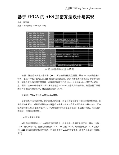
基于FPGA的AES加密算法设计与实现作者:窦贤振来源:《科技风》2019年第36期摘;要:通过分析高级加密标准(AES)算法的原理及其优越性,结合FPGA高度处理的特点,提出一种基于FPGA的AES加密算法实现方案。
采用了查找表方法优化了字节替代变换、列混合变换和密钥扩展模块,将设计的固核运行在Altera公司的Cyclone;II;FPGA芯片上,利用2块DE2硬件板和2台计算机搭建了一个AES加密文件传输平台,最后分析了设计的器件资源消耗和吞吐率,验证设计方案的可行性。
关键词:FPGA;查找表;AES;Verilog;HDL当前信息技术快速发展,用户对信息的采集、存储和传输的安全性能也逐渐提升要求。
利用数据加密算法,对数据进行加密来保障信息传输与存储的安全性则是有效地解决方法,而高级加密标准AES则是很好选择[1]。
本文给出的设计方案主要包括:系统整体结构、AES加解密模块、控制模块等部分。
1;AES加密算法原理AES加密过程是在一个4x4的位元组矩阵上,此矩阵是一个明文分组区块。
其中128位(bit)明文分为4列。
密鑰的长度包括:128、196以及256位。
矩阵列数包括:4、6以及8列。
AES算法为密钥迭代分组算法,包含轮函数对state的重复作用。
轮数大小取决于密钥长度[2]。
AES解密过程和加密过程互为逆运算,解密过程主要包含四个方面:逆行移位、逆字节替换、轮密钥加以及逆列混合。
AES加密需要Nb个字节的初始密钥及Nr轮迭代过程所需轮密钥,所以密钥生成算法需将初始密钥扩展为Nb(Nr+1)个字。
2;AES加密算法建模与设计系统整体结构主要包括:接口模块、AES加解密模块、串并转换和并串转换模块以及LCD显示模块。
通过硬件平台DE2的开关来选择工作模式,LCD显示屏显示系统“Mode:Encryption或Decryption”。
计算机通过串口将数据发送到DE2,接口模块收到数据后送到串并转换模块,处理后将数据发送到AES加解密模块,根据模式选择将数据送到相应模块,完成加密或者加密后将数据发送到并串转换模块,然后将数据发送到接口模块完成数据加密或解密。
基于FPGA的信息加密系统的设计与实现

基于FPGA的信息加密系统的设计与实现信息加密系统已经成为现代社会不可或缺的一部分,它可以保护数据的安全性,并且只有授权的人才可以访问敏感数据。
在过去,人们使用软件来实现加密,但随着科技的发展,硬件加密系统也变得越来越普及。
其中,基于FPGA的信息加密系统在其高速性、可编程性和低功耗等方面得到了广泛的应用。
本文将介绍一个基于FPGA的信息加密系统的设计与实现,包括加密算法的选择、系统架构的设计和关键技术的分析等内容。
一、加密算法的选择在设计一个基于FPGA的信息加密系统时,首先需要选择一个成熟的加密算法。
这里选择了AES算法作为核心加密算法。
AES算法是一种对称密钥加密算法,具有高速性和强大的安全性。
它的加密过程采用了分组密码的设计,将明文按照一定的规则分组加密,而密文则通过不断的子密钥加密得到。
为了进一步提高AES的安全性,可以加入其他算法作为补充,例如SM4算法、RSA算法等等。
二、系统架构的设计在确定了加密算法之后,接下来需要设计基于FPGA的信息加密系统的架构。
在本文中,我们采用了一种包含FPGA、RAM、Flash和外设等核心组件的架构。
具体来说,我们可以通过选择一款性能优良的FPGA芯片(例如Xilinx Kintex-7系列),并将其与高带宽的DDR3 RAM、大容量的Flash存储器以及各种外设(例如网卡、USB接口等等)相结合,形成一个完整的信息加密系统。
在设计系统架构时,需要考虑到以下因素:1. 性能:系统需要具有高速性,能够保证数据的快速加密和解密。
2. 可编程性:FPGA的可编程性使得系统可以满足不同的加密需求,并且方便进行升级和维护。
3. 安全性:系统需要具有强大的安全性,能够保护用户的数据免受攻击和窃取。
三、关键技术的分析在实现基于FPGA的信息加密系统时,还需要掌握一些关键技术。
以下是几个主要的技术点:1. 高速数据传输:为了保证系统的高速性,需要采用高速数据传输协议,如PCIe、Ethernet等等。
AES算法的FPGA实现
本栏目责任编辑:谢媛媛开发研究与设计技术随着计算机和通信网络的广泛应用,信息的安全性已受到人们的普遍重视。
信息安全己不仅仅局限于政治、军事以及外交等领域,而且也与人们的日常生活息息相关。
现在,密码学理论和技术已得到了迅速的发展,它是信息科学和技术中的一个重要研究领域。
1997年4月15日美国国家标准技术研究所NIST征集AES(AdvancedEncryptionStandard)算法,以取代DES。
DES密钥长度为56位,存在密钥过短的缺陷,3DES是一种由DES衍生出来的算法,虽然增加了密钥长度,但3DES的加密和解密时间消耗较大。
AES的基本要求是比3DES快,至少和3DES一样安全,分组长度128位,密钥长度为128位,192位,256位。
比利时密码专家JoanDaemen和VincentRijmen提出的"Rijndael数据加密算法”成为AES算法的标准。
经过多年来的分析和测试,至今没有发现AES的明显缺点,也没有找到明显的安全漏洞。
AES能够抵抗目前已知的各种攻击方法的攻击。
AES已于2002年生效,可以用软件也可以用硬件实现,实际使用中根据具体的应用环境两种情况都有。
软件实现是靠CPU的运算来实现算法,易受使用条件限制,加密速度慢,易受到破坏,影响数据传输质量。
硬件实现是用专用芯片实现密码算法,通过芯片对数据进行加密。
加密专用芯片是实现信息安全与保密的基础核心产品,具有高保密性高,加密速率高,易于实现复杂功能,易于嵌入总体成本低等优点,因此在复杂系统和大数据量加密系统中,一般都使用硬件来实现AES加密。
AES加密芯片网络通信安全方面有着广范的应用。
1有限域:简单的背景知识有限域的运算域F上的多项式形如:b(x)=bn-1xn-1+bn-2xn-2+b2x2+b1x+b0,x称为多项式的变元,bi是系数,而我们只需研究GF(2)即可,以一例说明GF(2)的表示例:十六进制数“57”对应的二进制数为01010111;看作一个字节,对应的多项式为x6+x4+x2+x+1。
AES加密算法的一种优化的FPGA实现方法

随着密码分析水平,芯片处理能力和计算技术的不断进步,DES的安全强度已经难以适应新的安全需要,其实现速度、代码大小和跨平台性均难以继续满足应用需求。
因此,NIST(美国国家标准与技术研究所)筹划AES(高级数据加密标准)算法,旨在取代DES,以保护21世纪敏感政府信息的新型加密标准。
Rijndael算法以其简洁、高效、安全和原则性的设计被接纳为AES,并于2001年11月26日正式公布在FIPS(Federal Information Processing Standards)出版的FIPS-PUB 197中。
作为DES的继承者,AES自从被接纳为标准之日起就已经被工业界、银行业和行政部门作为事实上的密码标准。
随着网络传输速度提升为gigabits数量级,业界对算法的执行速度的要求也越来越高,基于软件的密码算法便显得性能不足,需要采用硬件加密的方式,他采用一些特殊的优化技术(如流水线和查找表等),可极大地提高数据的流量并减少密钥的生成时间。
另外,用硬件实现加密算法及与之相关的密钥生成过程,并且封装到芯片中,因为他们不易被外部攻击者读取或更改,会有较高的物理安全性。
因此,基于硬件的密码算法就受到业界的普遍关注。
以FPGA为代表的可重构硬件以其自身所固有的特点——既具有硬件的安全性和高速性又有软件的灵活性和易维护性,已经成为分组密码算法硬件实现的热点研究方向。
本文介绍AES加密算法的一种FPGA实现的方法以及对其加密速度的优化处理技巧。
2 AES加密算法简介AES是一种迭代分组密码,采用的是代替/置换网络(SPN)。
他将明文分组长度固定为128 b,而且仅支持128,196或256 b的密钥长度,本文仅对密钥长度为128 b的情况进行讨论。
AES加密算法的实现包括密钥扩展过程和加密过程。
加密过程又包括一个作为初始轮的初始密钥加法(AddRoundKey),接着进行9次轮变换(Round),最后再使用一个轮变换(F inalRound),如图1所示。
基于FPGA先进加密算法(AES)的高速实现
基于FPGA先进加密算法(AES)的高速实现
沈启峰;黄士坦;杨靓
【期刊名称】《西安理工大学学报》
【年(卷),期】2006(022)002
【摘要】在介绍有限域的概念及Rijndael算法结构,详细分析算法中基于GF(28)加法、乘法运算过程的基础上,详细阐述了使用FPGA高速实现运算关键部分的设计思路.针对FPGA设计中对速度与面积两项指标的不同要求,分别给出了两种方案,最后,给出本算法在FPGA实现方式下的性能指标.通过与国内外部分相关测试数据比较,该优化算法的性能比(MBps/Slice)明显优于其它设计.
【总页数】4页(P203-206)
【作者】沈启峰;黄士坦;杨靓
【作者单位】西安微电子技术研究所,陕西,西安,710075;西安微电子技术研究所,陕西,西安,710075;西安微电子技术研究所,陕西,西安,710075
【正文语种】中文
【中图分类】TP3
【相关文献】
1.AES加密算法的FPGA高速实现 [J], 李田田;付宇卓
2.基于FPGA先进加密算法(AES)的并行实现 [J], 佟玉伟;陆浪如;李明;柯善学
3.基于FPGA的AES加密算法的高速实现 [J], 马肃;王击
4.高速先进加密算法(AES)IP核的VLSI实现 [J], 王晶;曾晓洋;陈俊;韩军
5.基于FPGA的AES加密算法设计与实现 [J], 窦贤振
因版权原因,仅展示原文概要,查看原文内容请购买。
AES加密的资源优化设计及FPGA实现
AES加密的资源优化设计及FPGA实现殷伟凤【期刊名称】《计算机与现代化》【年(卷),期】2012(0)11【摘要】This paper presents a compact hardware architecture for the AES algorithm which aims at reducing hardware resources without using a memory. The architecture only requires one combined S-box for encryption, decryption and key expansion which implements the multiplicative inverse in the composite field GF(24). In addition, the optimized combined MixColumns module has a lower gate count than other designs that implement mix columns operation. VHDL code is developed for the implementation of 128-bit data encryption with Device Cyclone of Altera Family.%针对目前广泛应用的低功耗低速嵌入式设备,以减少面积为目标,本文给出一个精简的实现AES加密算法的硬件结构.在字节置换模块的设计中,改进采用查找表的方法而只用组合逻辑实现,采用将GF(28)域中的元素映射为复合域GF(24)来求逆的方法,大量减少资源占用;对混合列计算进行优化设计;最后,采用Altera的Cyclone芯片基于VHDL语言实现AES加密算法,并给出仿真结果.【总页数】5页(P145-148,189)【作者】殷伟凤【作者单位】浙江传媒学院电子信息学院,浙江杭州310018【正文语种】中文【中图分类】TP309;TP368.1【相关文献】1.一种基于FPGA的AES加密算法优化设计 [J], 齐忠兵;李斌;王子复2.基于FPGA的AES加密算法设计与实现 [J], 窦贤振3.全通用AES加密算法的FPGA实现 [J], 李炽阳; 雷倩倩; 杨延飞4.AES加密算法的改进及FPGA实现 [J], 柴绍杰;张彩珍5.AES加密算法的FPGA优化设计 [J], 陈超因版权原因,仅展示原文概要,查看原文内容请购买。
基于FPGA快速AES算法IP核的设计与实现

基于FPGA快速AES算法IP核的设计与实现
李雪梅;欧海文;路而红;童新海
【期刊名称】《计算机工程与应用》
【年(卷),期】2006(42)24
【摘要】用硬件实现数据加密过程比软件实现更具有优势,已成为信息安全的主流方向.数据传输速度则是加密系统的一个重要指标.文章基于FPGA采用流水线技术和优化设计,提出了一种更高效的AES算法IP核的设计方法.在使用较低时钟频率的情况下,获得了更大的数据吞吐量和更快的传输速度.
【总页数】3页(P84-86)
【作者】李雪梅;欧海文;路而红;童新海
【作者单位】北京电子科技学院,北京,100070;北京电子科技学院,北京,100070;北京电子科技学院,北京,100070;北京电子科技学院,北京,100070
【正文语种】中文
【中图分类】TP311
【相关文献】
1.基于Xilinx FPGA IP核的浮点频域脉冲压缩算法的设计与实现 [J], 邢冠培;孟凡利
2.基于Xilinx FPGA IP核的浮点频域脉冲压缩算法的设计与实现 [J], 邢冠培;孟凡利
3.基于FPGA的AES算法硬件实现优化及IP核应用 [J], 龚向东;王佳;张准;王坤
4.基于FPGA的模板滤波IP核的设计与实现 [J], 李东;敖晟;田劲东;田勇
5.基于FPGA IP核的FIR滤波器设计与实现 [J], 李奇;尹倩;姚硕;孙杨
因版权原因,仅展示原文概要,查看原文内容请购买。
- 1、下载文档前请自行甄别文档内容的完整性,平台不提供额外的编辑、内容补充、找答案等附加服务。
- 2、"仅部分预览"的文档,不可在线预览部分如存在完整性等问题,可反馈申请退款(可完整预览的文档不适用该条件!)。
- 3、如文档侵犯您的权益,请联系客服反馈,我们会尽快为您处理(人工客服工作时间:9:00-18:30)。
AES on FPGA from the fastest to the smallestTim Good and Mohammed BenaissaDepartment of Electronic & Electrical Engineering,University of Sheffield, Mappin Street, Sheffield, S1 3JD, UK{t.good, m.benaissa}@Abstract. Two new FPGA designs for the Advanced Encryption Standard(AES) are presented. The first is believed to be the fastest, achieving 25 Gbpsthroughput using a Xilinx Spartan-III (XC3S2000) device. The second isbelieved to be the smallest and fits into a Xilinx Spartan-II (XC2S15) device,only requiring two block memories and 124 slices to achieve a throughput of2.2 Mbps. These designs show the extremes of what is possible and haveradically different applications from high performance e-commerce IPsecservers to low power mobile and home applications. The high speed designpresented here includes support for continued throughput during key changesfor both encryption and decryption which previous pipelined designs haveomitted.Keywords: Advanced Encryption Standard (AES), Field Programmable GateArray (FPGA), finite field, design exploration, high throughput, pipelined, lowarea, Application Specific Instruction Processor (ASIP).1. IntroductionThe research objective is to explore the design space associated with the Advanced Encryption Standard (AES) algorithm and in particular its Field Programmable Gate Array (FPGA) hardware implementation in terms of speed and area.The Rijndael cipher algorithm developed by Vincent Rijmen and Joan Daemen won the competition run by the US government (NIST) in 2000 to select a new commercial cryptographic algorithm and was accorded the accolade the Advanced Encryption Standard (AES). This algorithm is documented in the freely available US government publication, FIPS-197 [1].Subsequently, the AES has been the topic of much research to find suitable architectures for its hardware implementation. Architectural choices for a given application are driven by the system requirements in terms of speed and the resources consumed. This can simply be viewed as throughput and area, however, latency may also be important as may the cipher’s mode of operation. The FIPS-197 specification details a number of modes of operation for the cipher, for example, the simplest is the Electronic Code Book (ECB). Additional resilience to attack can be gained by using one of the feedback modes, for example, Output Feed Back (OFB) mode unfortunately such modes also limit the effectiveness of pipelining.2 Tim Good and Mohammed BenaissaThe use of FPGA has been expanding from its traditional role in prototyping to mainstream production. This change is being driven by commercial pressures to reduce design cost, risk and achieve a faster time to market. Advances in technology have resulted in mask programmed mass produced versions of FPGA fabrics being offered by the leading manufacturers which, for some applications, remove the necessity to move prototype designs from FPGA to ASIC whilst still achieving a low unit cost.Previous attempts [2,3] at high speed pipelined design have been to use what is an effectively ASIC number-of-gates-in-critical-path design flow to place the pipeline cuts. This is fine where the target device is an ASIC, however, does not result in optimal pipeline cut placement for a given FPGA fabric. This paper presents an alternative flow specific to FPGA which results in optimal pipeline placement thus increased performance. The new high speed design reported here achieves a throughput of 25 Gbps on a Xilinx Spartan-III FPGA and has applications in the area of hardware accelerators for IPsec servers.An additional novelty of the new high speed design presented in this paper is that the key may be periodically changed without loss of throughput and the operating mode may be changed between encryption and decryption at will. This enables the design to support a mode of operation where a batch of blocks may be encrypted or decrypted for each of a number of differently keyed concurrent channels without loss in throughput.Reported low area architectures [4,5] have been based around a 32-bit datapath. As the AES operations MixColumns and KeyExpansion are fundamentally 32-bit it was previously believed that this was optimal. An ASIC design by Feldhofer et al [6] used an 8-bit datapath married to a 32-bit MixColumns operator. However, even MixColumns may be rewritten in an 8-bit form accepting a higher control overhead and reduced throughput. To the authors’ knowledge, no 8-bit Application Specific Instruction Processor (ASIP) for AES has been reported in the literature. The results from the design of such a processor, which is believed to be the smallest, are documented in this paper. This design only occupies 60% of the smallest available Xilinx Spartan-II device (XC2S15) and achieves a throughput of 2.2 Mbps which is suitable for numerous applications in the mobile and home communications areas. This 8-bit design was compared to the two latest reported low area FPGA designs [4,5] which were based on a 32-bit architecture. Brief details of these designs are included together with their area cost results. A rival ‘PicoBlaze’ implementation is also presented as a benchmark to demonstrate the performance of a soft core microcontroller based design.This paper concludes with a discussion on the relative merits of each architecture. 2. The DesignThe intention here is to contrast a number of different architectures from the highest speed to the lowest area. An FPGA design flow is used throughout and performance results are presented together with comparison with the previously known best designs. The designs presented all support a 128-bit key. Xilinx ISE version 6.3 wasAES on FPGA from the fastest to the smallest 3 used for the design flow and the results quoted are from post place and route figures including all input and output delays. The new designs were coded in VHDL and validated using ModelSim.2.1 Fully Parallel Loop Unrolled ArchitectureFPGAs are particularly fast in terms of throughput when designs are implemented using deep pipeline cuts [2, 3, 7, 8, 9, 10, 11, 12]. The attainable speed is set by the longest path in the design so it is important to place the pipeline cuts such that the path lengths between the pipeline latches are balanced.First, the algorithm must be converted into a suitable form for deep pipelining [2,7]. This is achieved by removing all the loops to form a loop-unrolled design where the data is moved through the stationary execution resources. On each clock cycle, a new item of data is input and progresses over numerous cycles through the pipeline resulting in the output of data each cycle, however, with some unavoidable latency.One of the key optimisations was to express the SubBytes operation in computational form rather than as a look-up table. Earlier implementations used the look-up table approach (the “S” box) but this resulted in an unbreakable delay due to the time required pass through the FPGA block memories. The FIPS-197 specification provided the mathematical derivation for SubBytes in terms of Galois Field (28) arithmetic. This was efficiently exploited by hardware implementations using composite field arithmetic [2,7] which permitted a deeper level of pipelining thus improved throughput.The method of placement of pipeline latches (or cuts) was to consider the synthesis estimates for various units within the design. In particular, for Xilinx FPGAs, the number of cascaded 4-input LUTs in the critical path together with routing delays dominate the minimum cycle period. The first stage of optimisation is to consider the routing delay as constant and only consider change in the number of cascaded LUTs. In further optimisation design cycle iterations, the secondary effects of excessive routing delays and fan out load were considered.A simple function, such as the reduction-OR of a bit vector, can be used to generate LUT-levels versus cycle time results for the internal fabric of a specific technology. Table 1 shows such results for Xilinx Virtex-E. As can be seen from the table having pipeline registers between each LUT would yield the fastest design, however, there is a compromise in terms of the amount of fan-in required by the logic expressions in the design, the acceptable latency and realistic routing.4 Tim Good and Mohammed BenaissaLogic Levels Path Delay, ns Max Clock Freq, MHz1 2 3 4 5 6 7 8 2.1763.3214.4665.6116.7567.9019.04610.191459.6301.1223.9178.2148.0126.6110.598.1Table 1. Virtex-E performance versus logic levelsThe Virtex FPGA slice consists of two LUTs and one D-type flip-flop (FD) so a single level of logic between FDs would under utilise cells resulting in an approximate factor of two increase in the design area thus an impact on speed due to the larger distances. Similarly, two levels of logic between FDs would not provide sufficient flexibility (number of input terms in an expression) for the AES algorithm thus is likely to result in a significant increase of area. Further, with only two LUT levels routing, propagation time, fan-out and congestion from a lack of suitable routing resources are very likely to dominate the cycle time. This leaves three logic levels as the aiming point for pipeline register placement.There is a further complication in that the slice architecture includes a number of multiplexer (MUX) resources in addition to the LUTs these can be used to implement 2-input XOR and 2-input MUX functions without recourse to an extra level of LUTs. This factor must also be considered when placing the pipeline cuts.For a given set of pipeline cuts the synthesis results may be examined to verify that the critical path contains the correct number of cascaded LUTs. This design process yielded the following optimal cut set; Figure 1 shows the composite field implementation of SubBytes [2] followed by ShiftRows (SR) and MixColumns (M) operations. The number of LUT-levels is shown adjacent to each design unit and the total in a given pipeline step (represented by the dashed lines) at the bottom of the diagram. From an initial implementation it was found that additional time had to be allowed for the excessively long routing associated with the ShiftRows operation. Thus both the ShiftRows and its inverse require extra time compared to the remainder of the design. The excess time is approximately equivalent to a time associated with using two LUTs. The circuit shown can perform both encryption and decryption operations.AES on FPGA from the fastest to the smallest 5Fig. 1. Block diagram for each middle roundThe same treatment was given to the placement of pipeline cuts in the final round (Figure 2) which conveniently turned out to require one less cut than the middle rounds. This was used to accommodate the single cut required for the first round to yield a regular timing pattern.Fig. 2. Block diagram for final roundThe key expansion also required implementing and in some previous designs had been overlooked. One key design decision was how frequently the key must be changed and whether continued throughput is required. In this design, it was decided that throughput should be maintained during key changes and that it was desirable to change between encryption and decryption on each cycle with key changes made on similar order to the latency.The pipeline cuts chosen meant that a given data item will pass completely through the AES cipher in 70 cycles. One issue with the AES KeyExpansion is that the decryption process starts with the final RoundKey and the only method of obtaining the final RoundKey is to progress through the entire key expansion. This issue was resolved by having separate encryption and decryption RoundKey registers and the new key being supplied suitably in advance to its data (140 cycles). Although the additional registers occupy a sizable amount of area it does permit maintaining throughput during key changes. The KeyExpander takes 10 cycles to fully generate the required set of RoundKeys. In order to match the latency through the main6 Tim Good and Mohammed Benaissadatapath, the KeyExpander was placed in a separate clock domain running at 1/7 of the datapath clock. This allowed for many more levels of logic in the KeyExpander without it forming part of the critical path.The architecture for the KeyExpander is shown in Figure 3. The InvMixColumns unit (M-1) is included to maintain the order of the operations the same for both encryption and decryption. This is referred to in the FIPS-197 specification as “Equivalent Decryption”. There is no pipelining in the KeyExpander and it evaluates one RoundKey every clock cycle (in its clock domain). The “RCON” values, defined in the FIPS-197 specification, are computed using repeated finite field doubling (FFM2 unit). Four non-pipelined, forward transform only, versions of the SubBytes operation were implemented using composite field arithmetic (S units). The output RoundKeys are registered to permit correct operation given key changes and selection between encryption and decryption (rk1 to rk10 for encryption and dk1 to dk9 for decryption). The first RoundKey (rk0) is obtained by directly registering the key input.Fig. 3. Block Diagram of KeyExpander.AES on FPGA from the fastest to the smallest 7Fig. 4. Placement of design on Virtex-E (XCV2000E). DesignFPGA Part Freq. MHz Thro’put Mbps Latency ns Area slices Mbps / slice Data path Jarvinen et al [9]Virtex-E XCV1000e-8129.2 16,500 11,719 1.408 Enc Saggesse et al [10]Virtex-E XCV2000e-8158 20,300 5810 + 100B RAM 1.091 Enc Standaert et al [11]Virtex-E XCV3200e-8145 18,560 15,112 1.228 Enc Hodjat et al [3]Excl. key expand Virtex-II ProXC2VP20 169.1 21,640 420 9,446 Excl. KE2.290 Enc Zambreno et al [8]Virtex-II XC2V4000184.1 23,570 163 16,938 1.391 Enc Zhang (r=7), [2]Excl. key expand Virtex-E XCV1000E-8168.4 21,556 416 11,022Excl. KE1.956 Enc/ DecThis work, 3LUT cut, key change supportVirtex-E XCV2000E-8184.8 23,654 379 16,693 1.417 Enc/ Dec This work, 3LUT cut, key change support Spartan-III XC3S2000-5196.1 25,107 357 17,425 1.441 Enc/ Dec Table 2. Performance comparison of this work with previous designs.The placement of the design on a Virtex-E is shown in Figure 4 and the comparativeresults in Table 2. When comparing the quoted performance figures it is important torecognise the differences caused by changes in FPGA technology or more importantlywith the level of support for key agility, encryption and decryption. Some designs didnot include the key expansion in the results and other only supported the encryptiondatapath. This design shows an improvement in throughput over the previouslyknown best design [2] of approximately 10% using the same FPGA technology.However, further savings can be made by moving from the Virtex-E to the lower costSpartan-III devices with an increase in performance due to the more moderntechnology. The design achieves 25 Gbps throughput on the Spartan-III XC3S2000-5device.8 Tim Good and Mohammed BenaissaFurther improvement in throughput, of say 20%-30%, is possible by adopting a 2-LUT cut, however factors such as fanout and congestion are likely to be a significantobstacle to obtaining an improved throughput-area figure.Traditionally, such pipelined designs [3, 8, 9, 10, 11] only demonstrated any keyagility in encryption only modes such as Counter mode (CTR). However, this designsupports key agility for both encryption and decryption thus can support ElectronicCode Book (ECB) mode. In a multi channel environment the key can be changedonce ever 70 cycles thus support batch processing for a number of differently keyedconcurrent channels without loss in throughput.Further, it is a relatively simple task to extend the design by pipelining the keyexpansion, repeating its instantiation for all ten rounds and include registers(equivalent to approximately 15232 flip-flops) to support key changes each cycle.This would, in a multi channel environment, support any of the feedback modes,including Cipher Block Chaining (CBC) thus gaining improved security.2.2 Round based architecture using 32-bit DatapathThere already exist a number of good 32-bit based designs [4, 5, 13]. In these designsthe AES is implemented by breaking up a round into a number of smaller 32-bit wideoperations. Thus a number of cycles is required to complete each round.Such designs are based around a store for the “state” data (16 bytes for 128-bit)and look-up tables to perform the required AES operations of SubBytes andMixColumns. One of the optimisations documented in the FIPS-197 specification isto combine the look-up table for the MixColumns and SubBytes operation into asingle one. This is often referred to as the “T-box”.One of the key optimisations used by Rouvroy [5] was to exploit the larger (18kbit)block memories afforded by the Spartan-III and Virtex-II series FPGAs. This allowedfor 4 off 32 bit x 256 word look up tables (ROMs) to be implemented per (dual port)block memory. So the required number of 8 off 32 bit x 256 word lookup tables canbe implemented in two block memories, providing the four address buses needed (8-bits data in + 3-bits mode). The contents of the look up tables were chosen to provideconvenient access to SubBytes and InvSubBytes required by the key expander and thefinite field multiplications of the SubBytes table required for the combined SubBytes– MixColumns operation. The operation is completed by computing the exclusive-orof the four partial “T-box” values. The values stored are given by the followingexpression for the 8-bit value, a, using the SubBytes transformation and finite field multiplication by the given constant:⎥⎥⎥⎥⎥⎦⎤⎢⎢⎢⎢⎢⎣⎡••••••=)(11)(13)(9)(14)(3)()()(2)(a ISB a ISB a ISB a ISB a SB a ISB a SB a SB a T (1)A further block memory was used to store the RoundKeys together with severalmultiplexers to route the data and key.AES on FPGA from the fastest to the smallest 9 The following results (Table 3) were quoted together with a comparison with the previous design by Chadoweic and Gaj [4]. However, the figures quoted for throughput versus area failed to take into account the size of the block memories. This is of particular importance as the block memories on the Spartan-II are 4 kbit whereas those found on the Spartan-III and Virtex-II are 18 kbit. If these costs are taken into account then the result is substantially changed.The cost of using a block memory in terms of an equivalent number of slices is still a matter of some debate. One option would be to make the comparison based on the physical area occupied by a slice and a block memory but quotable figures are not forthcoming from the manufacturers. An alternative is to consider the number of slices required to implement the equivalent distributed memory, however, this varies depending on the functionality required (for example single or dual port). Such estimates vary between 8 and 32 bits/slice. For this analysis a worst case figure of 32 bits/slice was used. The relative merits of the various designs and thus conclusions remain unchanged when the analysis was repeated for the lower estimate.Chodowiec & Gaj [4] Rouvroyet al [5]Pramstalleret al [13]Rouvroyet al [5]Device XC2S30-6XC3S50-4XCV1000EXC2V40-6 Slices 2221631125146 Throughput(Mbps) 166 208 215 358RAM blocks 3 3 0 3Throughput / Area(kbps /slice) ignoring block ram750 1260 191 2450Bits of block ram used 9600 34176 0 34176Equiv slices for block ram 300 1068 0 1068Total equiv. slices (area) 522 1231 1125 1214Throughput / Area(kbps / slice)318 169 191 295Table 3. Performance of existing 32-bit FPGA designs2.3 Application Specific Processor Architecture using 8-bit DatapathThe objective was to develop a small AES implementation. One option was to usethe freely available Xilinx PicoBlaze soft core processor [14] for which the firstversion only requires 76 slices. However, for a practical design a small memory wasneeded thus the larger 96 slice KCPSM3 was selected. Additionally, the size of theROM required to implement 365 instructions for the AES had to be consideredtogether with an implementation for SubBytes. This results in a final design using thePicoBlaze of 119 slices plus the block memories which are accounted for here by anequivalent number of slices (once again 32 bits per slice was used). The resulting10 Tim Good and Mohammed Benaissadesign had an equivalent slice count of 452 and with a 90.2 MHz maximum clock. Key expansion followed by encipher took 13546 cycles and key expansion followed by decipher 18885 cycles. The average encipher-decipher throughput was 0.71 Mbps.An application specific instruction processor (ASIP) was developed based around an 8-bit datapath and minimal program ROM size. Minimisation of the ROM size resulted in a requirement to support subroutines and looping. This added area to the control portion of the design but the saving was made in terms of the size of the ROM. The total design, including an equivalent number of slices for the block memories only occupies 259 slices to give a throughput of 2.2Mbps.The datapath consisted of two processing units, the first to perform the SubBytes operation using resource shared composite field arithmetic and the second to perform multiply accumulate operations in Galois Field 28. A minimal set of instructions was developed (15 in total) to perform the operations required for the AES. The processor (Figure 5) used a pipelined design permitting execution of a new instruction every cycle.Fig. 5. ASIP ArchitectureFigure 6 is a pie chart depicting the balance of area between the various design units. Of the processor hardware approx 60% of the area is required for the datapath and 40% for the control.AES on FPGA from the fastest to thesmallest 113IndexedS-Box, 42I/O, 6ProgramFig. 6. Slice utilization versus design unitAs a good FPGA based 8-bit datapath for comparison could not be found, Table 4 shows comparison of this design with the state-of-the-art 32-bit designs using the relatively low cost Xilinx Spartan FPGAs. The two reference designs both quote throughput figures for a mode of operation where the key remains constant thus the time taken for key expansion was not included. A throughput figure was calculated for each design inclusive of the time taken for key expansion. The average for encipher and decipher was then calculated and is reported in Table 4 as the average throughput.This design Picoblaze based Chodowiec & Gaj [4] Rouvroy et al [5]FPGA Spartan-II XC2S15-6 Spartan-II XC2S15-6 Spartan-II XC2S30-6 Spartan-III XC3S50-4Clock Frequency (MHz) 67 90 60 71 Datapath Bits 8 8 32 32Slices 124 119 222 163 No. of Block RAMs used 2 2 3 3 Block RAM Size (kbits) 4 4 4 18 Bits of block RAM used 4480 10666 9600 34176 Est. equiv. slices for memory 140 333 300 1068 Total Equiv. Slices (area) 264 452 522 1231 Max Throughput (Mbps) - - 166 208 Ave. Throughput (Mbps) 2.2 0.71 69 87 Throughput/slice (kbps/slice) 8.3 1.9 132 70Summary Smallest Software Best speed/areaFastest Table 4. Comparison with other designs using low cost FPGAs12 Tim Good and Mohammed BenaissaFigure 7 shows the placement of this design on a Spartan-II (XC2S15) part. The design requires 124 slices and two block memories. One memory formed the program ROM and the second was used as the ASIP’s main memory (RAM). The AES application only required 360 bits of RAM thus the block memory was only partially utilized and could have be implemented as distributed memory with a cost of 42 additional slices and would then free up one of the block memories. There are also some concerns over the particular vulnerability of the block memories to power attacks so avoiding their use for key and data storage may be desirable. However, even avoiding use of the block memories does not negate such risks.Mul-AccSubBytesControllerFig. 7. Placement of low area design on Spartan-II (XC2S15)3 ConclusionsThis paper has presented a number of FPGA implementations from the fastest to the smallest. In terms of speed to area ratio the unrolled designs perform the best as there is no controller overhead. However, such designs are very large and need a 1 – 2 million gate device but achieve throughputs up to 25 Gbps. These designs have applications in fixed infrastructure such as IPsec for e-commerce servers.The low area design described here achieves 2.2 Mbps which is sufficient for most wireless and home applications. The area required is small thus fundamentally low power so has utility in the future mobile area. The design requires just over half the available resources of the smallest available Spartan-II FPGA.AES on FPGA from the fastest to the smallest 13 The advantage of the 8-bit ASIP over the more traditional 8-bit microcontroller architecture (PicoBlaze) is shown by the approximate factor of three improvement in throughput and 40% reduction in area (including estimated area for memories).The 32-bit datapath designs occupy the middle ground between the two extremes and have utility where moderate throughput in the 100 – 200 Mbps is required.The advantage of an FPGA specific optimisation over an ASIC number-of-gates approach has been demonstrated by the speed improvement made in the loop unrolled design.The best architectural decision is to select the design of the lowest possible area meeting the throughput and operating mode requirement for the system being developed. Figure 8 shows the different designs in terms of their throughput and area.Fig. 8. Throughput versus area for the different FPGA designs14 Tim Good and Mohammed Benaissa4 References[1] National Institute of Standards and Technology (NIST), Information TechnologyLaboratory (ITL), Advanced Encryption Standard (AES), Federal Information Processing Standards (FIPS) Publication 197, November 2001[2] X. Zhang, K. K. Parhi, High-speed VLSI architectures for the AES algorithm, IEEETrans. VLSI Systems, Vol. 12, Iss. 9, pp. 957 - 967, Sept. 2004[3] A. Hodjat, I. Verbauwhede, A 21.54 Gbits/s Fully Pipelined AES Processor on FPGA,12th Annual IEEE Sypmosium on Field-Programmable Custom Computing Machines (FCCM'04), pp. 308-309, April 2004[4] P. Chodowiec, K. Gaj, Very Compact FPGA Implementation of the AES Algorithm,Cryptographic Hardware and Embedded Systems (CHES 2003), LNCS Vol. 2779, pp.319 – 333, Springer-Verlag, October 2003[5] G. Rouvroy, F. X. Standaert, J. J. Quisquater, J. D. Legat, Compact and efficientencryption/decryption module for FPGA implementation of the AES Rijndael very well suited for small embedded applications, Procedings of the international conference on Information Technology: Coding and Computing 2004 (ITCC 2004), pp. 583 – 587, Vol. 2, April 2004[6] M. Feldhofer, S. Dominikus and J. Wolkerstorfer, Strong Authentication for RFIDSystems Using the AES Algorithm, CHES 2004, LNCS 3156, pp. 357-370, Springer-Verlag, 2004.[7] A. Satoh, S. Morioka, K. Takano, S. Munetoh, A Compact Rijndael HardwareArchitecture with S-Box Optimization, Proceedings of ASIACRYPT 2001, LNCS Vol.2248, pp. 239 - 254, Springer-Verlag, December 2001[8] J. Zambreno, D. Nguyen, A. Choudhary, Exploring Area/Delay Trade-offs in an AESFPGA Implementation, Proc. FPL 2004, 2004[9] K. U. Jarvinen, M. T. Tommiska, and J. O. Skytta, A fully pipelined memoryless 17.8Gbps AES-128 encryptor, Proc. Int. Symp. Field-Programmable Gate Arrays (FPGA 2003), Monterey, CA, pp. 207–215, Feb. 2003[10] G. P. Saggese, A. Mazzeo, N. Mazocca, and A. G. M. Strollo, An FPGA basedperformance analysis of the unrolling, tiling and pipelining of the AES algorithm, Proc.FPL 2003, Portugal, Sept. 2003.[11] F. Standaert, G. Rouvroy, J. Quisquater, and J. Legat, Efficient implementation ofRijndael encryption in reconfigurable hardware: Improvements & design tradeoffs, Proc. CHES 2003, Cologne, Germany, Sept. 2003.[12] M. McLoone and J.V. McCanny, High Performance Single-Chip FPGA RijndaelAlgorithm Implementations, CHES 2001, Paris, France, 2001[13] N. Pramstaller and J. Wolkerstorfer, A Universal and efficient AES co-processor forField Programmable Logic Arrays, FPL 2004, LNCS Vol. 3203, pp. 565-574, Springer-Verlag, 2004.[14] K. Chapman, PicoBlaze 8-bit Microcontroller, Xilinx, 2002/products/design_resources/proc_central/grouping/picoblaze.htm 5 AcknowledgementThis work was funded by the UK Engineering and Physical Sciences Research Council (EPSRC).。
