SN03A_Datasheet_创裕
2n3903数据表说明书

DATA SHEET General PurposeTransistorsNPN Silicon2N3903, 2N3904Features•Pb−Free Packages are Available*MAXIMUM RATINGSRating Symbol Value UnitCollector−Emitter Voltage V CEO40VdcCollector−Base Voltage V CBO60VdcEmitter−Base Voltage V EBO 6.0VdcCollector Current − Continuous I C200mAdcTotal Device Dissipation @ T A = 25°CDerate above 25°C P D6255.0mWmW/°CTotal Device Dissipation@ T C = 25°C Derate above 25°C P D1.512WmW/°COperating and Storage Junction Temperature Range T J, T stg−55 to +150°CTHERMAL CHARACTERISTICS (Note 1)Characteristic Symbol Max Unit Thermal Resistance, Junction−to−Ambient R q JA200°C/W Thermal Resistance, Junction−to−Case R q JC83.3°C/W Stresses exceeding those listed in the Maximum Ratings table may damage the device. If any of these limits are exceeded, device functionality should not be assumed, damage may occur and reliability may be affected.1.Indicates Data in addition to JEDEC Requirements.*For additional information on our Pb−Free strategy and soldering details, please download the onsemi Soldering and Mounting T echniques Reference Manual, SOLDERRM/D.MARKING DIAGRAMSSee detailed ordering and shipping information in the package dimensions section on page 3 of this data sheet.ORDERING INFORMATIONCOLLECTOR21EMITTER2N390xYWW GGx= 3 or 4Y= YearWW= Work WeekG= Pb−Free Package(Note: Microdot may be in either location)BENT LEADTAPE & REELAMMO PACKSTRAIGHT LEADBULK PACKTO−92CASE 29STYLE 1ELECTRICAL CHARACTERISTICS (T A = 25°C unless otherwise noted)Characteristic Symbol Min Max Unit OFF CHARACTERISTICSCollector−Emitter Breakdown Voltage (Note 2)(I C = 1.0 mAdc, I B = 0)V(BR)CEO40−Vdc Collector−Base Breakdown Voltage (I C = 10 m Adc, I E = 0)V(BR)CBO60−Vdc Emitter−Base Breakdown Voltage (I E = 10 m Adc, I C = 0)V(BR)EBO 6.0−Vdc Base Cutoff Current (V CE = 30 Vdc, V EB = 3.0 Vdc)I BL−50nAdc Collector Cutoff Current (V CE = 30 Vdc, V EB = 3.0 Vdc)I CEX−50nAdc ON CHARACTERISTICSDC Current Gain (Note 2)(I C = 0.1 mAdc, V CE = 1.0 Vdc)2N39032N3904 (I C = 1.0 mAdc, V CE = 1.0 Vdc)2N39032N3904 (I C = 10 mAdc, V CE = 1.0 Vdc)2N39032N3904 (I C = 50 mAdc, V CE = 1.0 Vdc)2N39032N3904 (I C = 100 mAdc, V CE = 1.0 Vdc)2N39032N3904h FE204035705010030601530−−−−150300−−−−−Collector−Emitter Saturation Voltage (Note 2) (I C = 10 mAdc, I B = 1.0 mAdc)(I C = 50 mAdc, I B = 5.0 mAdc V CE(sat)−−0.20.3VdcBase−Emitter Saturation Voltage (Note 2) (I C = 10 mAdc, I B = 1.0 mAdc)(I C = 50 mAdc, I B = 5.0 mAdc)V BE(sat)0.65−0.850.95VdcSMALL−SIGNAL CHARACTERISTICSCurrent−Gain − Bandwidth Product(I C = 10 mAdc, V CE = 20 Vdc, f = 100 MHz)2N39032N3904f T250300−−MHzOutput Capacitance (V CB = 5.0 Vdc, I E = 0, f = 1.0 MHz)C obo− 4.0pF Input Capacitance (V EB = 0.5 Vdc, I C = 0, f = 1.0 MHz)C ibo−8.0pFInput Impedance(I C = 1.0 mAdc, V CE = 10 Vdc, f = 1.0 kHz)2N39032N3904h ie1.01.08.010k WVoltage Feedback Ratio(I C = 1.0 mAdc, V CE = 10 Vdc, f = 1.0 kHz)2N39032N3904h re0.10.55.08.0X 10−4Small−Signal Current Gain(I C = 1.0 mAdc, V CE = 10 Vdc, f = 1.0 kHz)2N39032N3904h fe50100200400−Output Admittance (I C = 1.0 mAdc, V CE = 10 Vdc, f = 1.0 kHz)h oe 1.040m mhosNoise Figure(I C = 100 m Adc, V CE = 5.0 Vdc, R S = 1.0 k W, f = 1.0 kHz)2N39032N3904NF−−6.05.0dBSWITCHING CHARACTERISTICSDelay Time(VCC = 3.0 Vdc, V BE = 0.5 Vdc,I C = 10 mAdc, I B1 = 1.0 mAdc)t d−35nsRise Time t r−35nsStorage Time(V CC = 3.0 Vdc, I C = 10 mAdc,2N3903I B1 = I B2 = 1.0 mAdc)2N3904t s−−175200nsFall Time t f−50ns 2.Pulse Test: Pulse Width v 300 m s; Duty Cycle v 2%.ORDERING INFORMATIONDevicePackage Shipping †2N3903RLRM TO −922000 / Ammo Pack 2N3904TO −925000 Units / Bulk 2N3904G TO −92(Pb −Free)5000 Units / Bulk 2N3904RLRA TO −922000 / Tape & Reel 2N3904RLRAG TO −92(Pb −Free)2000 / Tape & Reel 2N3904RLRM TO −922000 / Ammo Pack 2N3904RLRMG TO −92(Pb −Free)2000 / Ammo Pack 2N3904RLRPTO −922000 / Ammo Pack 2N3904RLRPG TO −92(Pb −Free)2000 / Ammo Pack 2N3904RL1G TO −92(Pb−Free)2000 / Tape & Reel 2N3904ZL1TO −922000 / Ammo Pack 2N3904ZL1GTO −92(Pb −Free)2000 / Ammo Pack†For information on tape and reel specifications, including part orientation and tape sizes, please refer to our Tape and Reel Packaging Specifications Brochure, BRD8011/D.Figure 1. Delay and Rise Time Equivalent Test CircuitFigure 2. Storage and Fall Time Equivalent Test Circuit10 < t 1 < 500 m * T otal shunt capacitance of test jig and connectors* T otal shunt capacitance of test jig and connectorsTYPICAL TRANSIENT CHARACTERISTICSFigure 3. CapacitanceREVERSE BIAS VOLTAGE (VOLTS)2.03.05.07.0101.00.1Figure 4. Charge DataI C , COLLECTOR CURRENT (mA)50001.0Q , C H A R G E (p C )3000200010005003002007001005070 2.0 3.0 5.07.01020305070100200C A P A C I T A N C E (p F )1.02.03.0 5.07.010200.20.30.50.7T J = 25°C T J = 125°CFigure 5. Turn −On TimeI C , COLLECTOR CURRENT (mA)7010020030050050Figure 6. Rise TimeI C , COLLECTOR CURRENT (mA)T I M E (n s )5t , R I S E T I M E (n s )Figure 7. Storage Time I C , COLLECTOR CURRENT (mA)Figure 8. Fall TimeI C , COLLECTOR CURRENT (mA)1030720701002003005005051030720701002003005005051030720701002003005005051030720r t , F A L L T I M E (n s )f t , S T O R A G E T I M E (n s )s ′TYPICAL AUDIO SMALL −SIGNAL CHARACTERISTICSNOISE FIGURE VARIATIONS(V CE = 5.0 Vdc, T A = 25°C, Bandwidth = 1.0 Hz)Figure 9. f, FREQUENCY (kHz)46810122Figure 10.R S , SOURCE RESISTANCE (k OHMS)0N F , N O I S E F I G U R E (d B )04681012214N F , N O I S E F I G U R E (d B )Figure 11. Current GainI C , COLLECTOR CURRENT (mA)7010020030050Figure 12. Output AdmittanceI C , COLLECTOR CURRENT (mA)h , C U R R E N T G A I Nh , O U T P U T A D M I T T A N C E ( m h o s )Figure 13. Input Impedance I C , COLLECTOR CURRENT (mA)Figure 14. Voltage Feedback RatioI C , COLLECTOR CURRENT (mA)3010050510202.03.05.07.0101.00.10.21.02.0 5.00.5100.30.5 3.00.72.05.010201.00.20.5o e h , V O L T A G E F E E D B A C K R A T I O (X 10 )r e h , I N P U T I M P E D A N C E (k O H M S )ie 0.10.21.02.0 5.0100.30.5 3.00.10.21.02.0 5.0100.30.5 3.0210.10.21.02.0 5.0100.30.5 3.0f e m -4h PARAMETERS(V CE = 10 Vdc, f = 1.0 kHz, T A = 25°C)TYPICAL STATIC CHARACTERISTICSFigure 15. DC Current GainI C , COLLECTOR CURRENT (mA)0.30.50.71.02.00.2h , D C C U R R E N T G A I N (N O R M A L I Z E D )0.1F EFigure 16. Collector Saturation RegionI B , BASE CURRENT (mA)0.40.60.81.00.2V , C O L L E C T O R E M I T T E R V O L T A G E (V O L T S )0CE Figure 17. “ON” Voltages I C , COLLECTOR CURRENT (mA)0.40.60.81.01.20.2Figure 18. Temperature CoefficientsI C , COLLECTOR CURRENT (mA)V , V O L T A G E (V O L T S )- 0.500.51.0C O E F F I C I E N T (m V / C )- 1.0- 1.5- 2.0°TO−92 (TO−226)CASE 29−11ISSUE AMDATE 09 MAR 2007STYLES ON PAGE 2NOTES:1.DIMENSIONING AND TOLERANCING PER ANSIY14.5M, 1982.2.CONTROLLING DIMENSION: INCH.3.CONTOUR OF PACKAGE BEYOND DIMENSION RIS UNCONTROLLED.4.LEAD DIMENSION IS UNCONTROLLED IN P ANDBEYOND DIMENSION K MINIMUM.SECTION X−XPLANE DIM MIN MAX MIN MAXMILLIMETERSINCHESA0.1750.205 4.45 5.20B0.1700.210 4.32 5.33C0.1250.165 3.18 4.19D0.0160.0210.4070.533G0.0450.055 1.15 1.39H0.0950.105 2.42 2.66J0.0150.0200.390.50K0.500---12.70---L0.250--- 6.35---N0.0800.105 2.04 2.66P---0.100--- 2.54R0.115--- 2.93---V0.135--- 3.43---BENT LEADTAPE & REELAMMO PACKSTRAIGHT LEADBULK PACKNOTES:1.DIMENSIONING AND TOLERANCING PERASME Y14.5M, 1994.2.CONTROLLING DIMENSION: MILLIMETERS.3.CONTOUR OF PACKAGE BEYONDDIMENSION R IS UNCONTROLLED.4.LEAD DIMENSION IS UNCONTROLLED IN PAND BEYOND DIMENSION K MINIMUM.SECTION X−XDIM MIN MAXMILLIMETERSA 4.45 5.20B 4.32 5.33C 3.18 4.19D0.400.54G 2.40 2.80J0.390.50K12.70---N 2.04 2.66P 1.50 4.00R 2.93---V 3.43---STRAIGHT LEADBULK PACKBENT LEADTAPE & REELAMMO PACKMECHANICAL CASE OUTLINEPACKAGE DIMENSIONSTO−92 (TO−226)CASE 29−11ISSUE AMDATE 09 MAR 2007STYLE 1:PIN 1.EMITTER2.BASE3.COLLECTORSTYLE 6:PIN 1.GATE2.SOURCE & SUBSTRATE3.DRAINSTYLE 11:PIN 1.ANODE2.CATHODE & ANODE3.CATHODESTYLE 16:PIN 1.ANODE2.GATE3.CATHODESTYLE 21:PIN 1.COLLECTOR2.EMITTER3.BASESTYLE 26:PIN 1.V CC2.GROUND 23.OUTPUTSTYLE 31:PIN 1.GATE2.DRAIN3.SOURCE STYLE 2:PIN 1.BASE2.EMITTER3.COLLECTORSTYLE 7:PIN 1.SOURCE2.DRAIN3.GATESTYLE 12:PIN 1.MAIN TERMINAL 12.GATE3.MAIN TERMINAL 2STYLE 17:PIN 1.COLLECTOR2.BASE3.EMITTERSTYLE 22:PIN 1.SOURCE2.GATE3.DRAINSTYLE 27:PIN 1.MT2.SUBSTRATE3.MTSTYLE 32:PIN 1.BASE2.COLLECTOR3.EMITTERSTYLE 3:PIN 1.ANODE2.ANODE3.CATHODESTYLE 8:PIN 1.DRAIN2.GATE3.SOURCE & SUBSTRATESTYLE 13:PIN 1.ANODE 12.GATE3.CATHODE 2STYLE 18:PIN 1.ANODE2.CATHODE3.NOT CONNECTEDSTYLE 23:PIN 1.GATE2.SOURCE3.DRAINSTYLE 28:PIN 1.CATHODE2.ANODE3.GATESTYLE 33:PIN 1.RETURN2.INPUT3.OUTPUTSTYLE 4:PIN 1.CATHODE2.CATHODE3.ANODESTYLE 9:PIN 1.BASE 12.EMITTER3.BASE 2STYLE 14:PIN 1.EMITTER2.COLLECTOR3.BASESTYLE 19:PIN 1.GATE2.ANODE3.CATHODESTYLE 24:PIN 1.EMITTER2.COLLECTOR/ANODE3.CATHODESTYLE 29:PIN 1.NOT CONNECTED2.ANODE3.CATHODESTYLE 34:PIN 1.INPUT2.GROUND3.LOGICSTYLE 5:PIN 1.DRAIN2.SOURCE3.GATESTYLE 10:PIN 1.CATHODE2.GATE3.ANODESTYLE 15:PIN 1.ANODE 12.CATHODE3.ANODE 2STYLE 20:PIN 1.NOT CONNECTED2.CATHODE3.ANODESTYLE 25:PIN 1.MT 12.GATE3.MT 2STYLE 30:PIN 1.DRAIN2.GATE3.SOURCESTYLE 35:PIN 1.GATE2.COLLECTOR3.EMITTERON Semiconductor and are registered trademarks of Semiconductor Components Industries, LLC (SCILLC). SCILLC reserves the right to make changes without further notice to any products herein. SCILLC makes no warranty, representation or guarantee regarding the suitability of its products for any particular purpose, nor does SCILLC assume any liability arising out of the application or use of any product or circuit, and specifically disclaims any and all liability, including without limitation special, consequential or incidental damages.“Typical” parameters which may be provided in SCILLC data sheets and/or specifications can and do vary in different applications and actual performance may vary over time. All operating parameters, including “Typicals” must be validated for each customer application by customer’s technical experts. SCILLC does not convey any license under its patent rights nor the rights of others. SCILLC products are not designed, intended, or authorized for use as components in systems intended for surgical implant into the body, or other applications intended to support or sustain life, or for any other application in which the failure of the SCILLC product could create a situation where personal injury or death may occur. Should Buyer purchase or use SCILLC products for any such unintended or unauthorized application, Buyer shall indemnify and hold SCILLC and its officers, employees, subsidiaries, affiliates, and distributors harmless against all claims, costs, damages, and expenses, and reasonable attorney fees arising out of, directly or indirectly, any claim of personal injury or deathassociated with such unintended or unauthorized use, even if such claim alleges that SCILLC was negligent regarding the design or manufacture of the part. SCILLC is an EqualPUBLICATION ORDERING INFORMATIONTECHNICAL SUPPORTNorth American Technical Support:LITERATURE FULFILLMENT :Email Requests to:*******************Europe, Middle East and Africa Technical Support:。
Amtech Tacky 助焊膏系列安全数据表说明书

Inventec Performance Chemicals USA, LLCSAFETY DATA SHEET (SDS)SECTION 1: PRODUCT AND COMPANY IDENTIFICATIONPRODUCT NAME: Amtech Tacky Paste Flux Series: 200, 400, 500, 600, 4000, SynTECH, WSFC-305L and #61 SYNONYMS:Tacky FluxMANUFACTURER: Inventec Performance Chemicals USA, LLCADDRESS:PO Box 989 Deep River, CT 06417 USAPHONE:860-526-8300FAX:860-526-8243EMERGENCY:Infotrac-(800)535-5035REVISION DATE:December 19, 2014REVISION DATE: 3DOCUMENT NAME:SDS-Tacky Flux-008PRODUCT USE:Bonding solder joints in production and repair of circuit boardsSECTION 2: HAZARDS IDENTIFICATIONCHEMICAL NAME:N/ACHEMICAL FAMILY:MixtureCHEMICAL FORMULA:N/AROUTES OF ENTRY: Inhalation, Ingestion, Skin/Eye ContactGHS:Signal Word: WarningHazard statement(s)H302 Harmful if swallowedH317 May cause an allergic skin reactionH320 Causes eye irritationH335 May cause respiratory irritationPrecautionary statement(s)P102 Keep out of reach of childrenP233 Keep container tightly closedP264 Wash hands thoroughly after handlingP270 Do not eat, drink or smoke when using this productP280 Wear protective gloves/protective clothing/eye protection/face protectionP302+P352 IF ON SKIN: Wash with plenty of soap and waterP305+P351 IF IN EYES: Rinse continuously with water for several minutesP404 Store in a closed containerP501 Dispose of contents/containers in accordance with Federal, State/Provincial, and/or local regulations POTENTIAL HEALTH EFFECTS:EYE CONTACT: May cause moderate irritation. Do not allow material to come in contact with eyes.SKIN CONTACT: May cause moderate skin irritation.INHALATION: May cause irritation to the respiratory tract.INGESTION: Harmful if swallowed. May cause irritation to the mouth, throat, and stomach. May cause abdominal discomfort, nausea, vomiting, and/or diarrhea.CHRONIC: Not established.SECTION 2 NOTES:Inventec Performance Chemicals USA, LLC does not recommend, manufacture, market, or endorse any of its products for human consumption.SECTION 3: COMPOSITION/INFORMATION ON INGREDIENTSIngredient CAS Number Exposure LimitsModified Rosins N/A N/APine Oil Derivatives 8000-41-7 N/AProprietary Ingredients N/A N/AMixed Carboxylic Acids N/A N/ASECTION 3 NOTES:Percentages of individual components are not listed as this information is considered a trade secret.SECTION 4: FIRST AID MEASURESEYES: Flush with plenty of water, contact a physician. If contact lenses can be removed easily, flush eyes without contact lenses. SKIN: Wash affected area with plenty of warm, soapy water. If irritation persists, seek medical attention.INGESTION: Call a physician or Poison Control Center immediately. Do not induce vomiting.INHALATION: Remove to fresh air. If not breathing, seek immediate medical attention.SECTION 5: FIRE-FIGHTING MEASURESEXTINGUISHING MEDIA: Dry chemical, foamSPECIAL FIRE FIGHTING PROCEDURES: Do not use water. Use NIOSH-approved self-contained Breathing Apparatusand full protective clothing if involved in a fire.UNUSUAL FIRE AND EXPLOSION HAZARDS:This product does not present any unusual fire and explosion hazards. SECTION 6: ACCIDENTAL RELEASE MEASURESACCIDENTAL RELEASE MEASURES: If material spills or leaks, collect and place into a properly labeled waste container. Remove traces of tacky flux using cloth rags or paper towels moistened with Isopropyl Alcohol. Follow on-site personal protective equipment recommendations.SECTION 6 NOTES:See Sections 2, 4, and 7 for additional information.SECTION 7: HANDLING AND STORAGEHANDLING/STORAGE: Keep containers tightly closed when not in use. Use care to avoid spills. Avoid inhalation of fumes or dust. Avoid contact with eyes, skin, and clothing.OTHER PRECAUTIONS: Empty containers may retain product residues in vapor, liquid, and/or solid form. All labeled hazard precautions should be observed.WORK HYGIENIC PRACTICES: Cosmetics/Food/Drink/Tobacco should not be consumed or used in work areas. Always wash hands after handling material and before applying or using cosmetics/food/drink/tobacco.SECTION 7 NOTES:For industrial use only.SECTION 8: EXPOSURE CONTROLS/PERSONAL PROTECTIONVENTILATION: Provide sufficient mechanical (general and/or local exhaust) ventilation to maintain exposure below TLVs. RESPIRATORY PROTECTION: Use with adequate ventilation.EYE PROTECTION: Use with appropriate safety glasses.SKIN PROTECTION: Protective gloves and clothing should be worn when handling material. Wash hands thoroughly with soap and water upon leaving the work area.SECTION 9: PHYSICAL AND CHEMICAL PROPERTIESAPPEARANCE: Clear, White, or Yellow to Dark Amber gelODOR: Mild odorODOR THRESHOLD: Not establishedpH as SUPPLIED: N/ASECTION 9: PHYSICAL AND CHEMICAL PROPERTIES (continued)MELTING POINT: Not establishedFREEZING POINT: Not establishedINITIAL BOILING POINT: Not establishedBOILING RANGE: Not establishedFLASH POINT: Not establishedEVAPORATION RATE: Not establishedFLAMMABILITY (solid): Not establishedUPPER/LOWER FLAMMABILITY: Not establishedUPPER/LOWER EXPLOSIVE LIMITS:Not establishedVAPOR PRESSURE (mmHg): N/A (°F/°C)VAPOR DENSITY (AIR = 1): N/A (°F/°C)RELATIVE DENSITY: Not establishedSOLUBILITY IN WATER: PartiallyPARTITION COEFFICIENT (n-octanol/water): Not establishedAUTOIGNITION TEMPERATURE: Not establishedDECOMPOSITION TEMPERATURE: Not establishedVISCOSITY: N/A (°F/°C)SECTION 10: STABILITY AND REACTIVITYSTABILITY: StableCONDITIONS TO AVOID (STABILITY): Freezing temperatures. High temperatures. INCOMPATIBILITY (MATERIAL TO AVOID): Strong oxidizing materialsHAZARDOUS DECOMPOSITION/BY-PRODUCTS: Harmful organic fumes and toxic oxide fumes may form at elevatedtemperatures.POSSIBILITY OF HAZARDOUS REACTIONS: Will not occurSECTION 11: TOXICOLOGICAL INFORMATIONACUTE TOXICITY: Not availableSKIN CORRISION/IRRITATION: Not establishedSERIOUS EYE DAMAGE/IRRITATION: Not availableRESPIRATORY OR SKIN SENSITIZATION: Not establishedGERM CELL MUTAGENICITY: Not availableCARCINOGENICITY: Not availableREPRODUCTIVE TOXICITY: Not availableSTOT-SINGLE EXPOSURE: Not availableSTOT-REPEATED EXPOSURE: Not availableASPIRATION HAZARD: Not availableSECTION 12: ECOLOGICAL INFORMATIONTOXICITY: Product not testedPERSISTENCE AND DEGRADIBILITY: Product not testedBIOACCUMULATIVE POTENTIAL: Product not testedMOBILITY IN SOIL: Product not testedOTHER ADVERSE EFFECTS: Product not testedSECTION 13: DISPOSAL CONSIDERATIONSWASTE DISPOSAL METHOD: Scrap and waste solder should be stored in a dry, sealed container for later disposal. Disposal must be in accordance with Federal, State/Provincial, and Local Regulations.SECTION 14: TRANSPORT INFORMATIONTransport in accordance with applicable regulations and requirements.UN Number: Not availableUN Proper Shipping Name: Not availablePackaging Group:Not applicableEnvironmental Hazards:NoneTRANSPORT HAZARD CLASSES:US DOT Hazardous Material Classification: Tacky Flux is not listed as a DOT hazardous materialWater Transportation: Tacky Flux is not listed as a hazardous materialIATA Hazardous Material Classification: Tacky Flux is not listed as IATA hazardous materialSECTION 15: REGULATORY INFORMATIONAll ingredients used to manufacture this product are listed on the EPA TSCA Inventory.U.S. FEDERAL REGULATIONS: Not regulatedSTATE REGULATIONS: Not regulatedINTERNATIONAL REGULATIONS: Not regulatedSECTION 16: OTHER INFORMATIONHMIS Rating: Health=1 Flammability=1 Physical Hazard=0 Personal Protection=X KEY:N/A: Not applicableGHS: Global Harmonized SystemOSHA: Occupational Safety and Health AdministrationACGIH: American Conference of Governmental Industrial HygienistsNTP: National Toxicology ProgramIARC: International Agency for Research on CancerCAS: Chemical Abstract ServiceNIOSH: National Institute for Occupational Safety & HealthSTOT: Specific target organ toxicityTLV: Threshold limit valueUS DOT: United States Department of TransportationDOT: Department of TransportationIATA: International Air Transport AssociationEPA:Environmental Protection AgencyTSCA:Toxic Substance Control ActHMIS:Hazardous Material Identification SystemPREPARATION INFORMATION:This update supersedes all previously released documents.PREPARED BY: Wendy W. GesickAPPROVED BY: Leigh W. GesickDISCLAIMER:The information contained herein is based on data considered to be accurate but does not purport to be all-inclusive and shall be used only as a guide. No warranty is expressed or implied regarding the accuracy of this data and Inventec Performance Chemicals USA, LLC shall not be held liable for any damage resulting from any handling or contact with the above product. Liability is expressly disclaimed for loss or injury arising out of use of this information or the use of any materials designated. This material is not for resale, unauthorized distribution, or personal use.。
MM3513A01NRH_规格书_100914
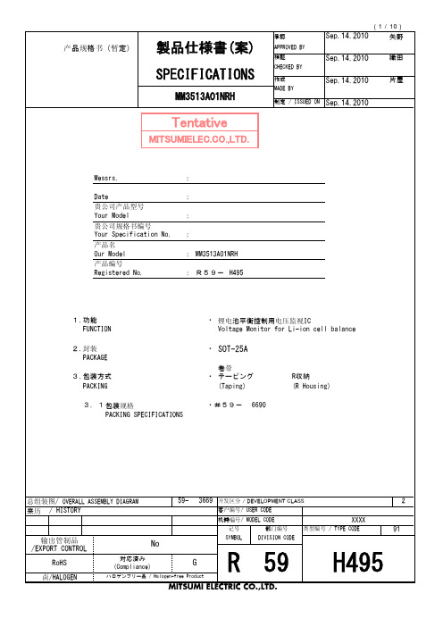
1.功能 FUNCTION
2.封装 PACKAGE
3.包装方式 PACKING
3.1 包装规格 PACKING SPECIFICATIONS
・ 锂电池平衡控制用电压监视IC Voltage Monitor for Li-ion cell balance
・ SOT-25A
卷带 ・ テーピング
(Taping)
℃
9. 电气特性 Electrical characteristics
项目 Parameter 动作输入电压 Operating input voltage
记号 Symbol VDD1
条件 Conditions VDD-VSS
最小 Min.
1.5
标准 Typ.
-
Topr=25℃
最大 Max.
单位 Unit
0.005 0.010 0.015 V C
T=25℃ VDD=3.4V→4.6V
0.20 0.25 0.30 s C
检测延时时间 Detection delay time
tVdet
T=-5~60℃
*4
VDD=3.4V→4.6V
0.18
0.25 0.33
s
C
T=-30~70℃ *4 VDD=3.4V→4.6V
检测电压 Detection voltage
*3
Vdet
T=-5~60℃ R1=330Ω
*4 4.125 4.150 4.175 V C
T=-30~70℃ R1=330Ω
*4 4.105 4.150 4.195 V
C
滞后电压 Hysteresis voltage
*3
Vhys
T=-30~70℃ R1=330Ω
Murata LQW03AW_00系列芯片电容器(芯片导纳)参考规格书说明书
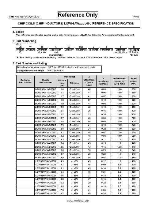
CHIP COILS (CHIP INDUCTORS) LQW03AW□□□□00□ REFERENCE SPECIFICATION1. ScopeThis reference specification applies to chip coils (chip inductors) LQW03AW_00 series for general electronic equipment.2. Part Numbering(Ex.)LQ W 03 A W 5N4 J 0 0 DProductID Structure Dimension(L × W)ApplicationandcharacteristicCategory Inductance Tolerance Performance ElectrodespecificationPackagingD: taping*B: bulk*B: Bulk packing is also available (taping condition: however, products without reels are put in plastic bags).3. Part Number and RatingOperating temperature range -55°C to +125°C (including self-generated heat)Storage temperature range -55°C to +125°CCustomer Part numberMurataPart numberInductance Q(900 MHz)(Typicalvalue)DCresistance(Ω max.)Self-resonantfrequency(GHz min.)Ratedcurrent(mA) Nominalvalue(nH)ToleranceLQW03AW1N0C00D1.0C:±0.2nH 48 0.03 19.0 900 LQW03AW1N1C00D1.1C:±0.2nH 41 0.06 19.0 660 LQW03AW1N7C00D1.7C:±0.2nH 41 0.07 19.0 600 LQW03AW1N8C00D1.8C:±0.2nH 37 0.10 19.0 520 LQW03AW1N9C00D1.9C:±0.2nH 41 0.08 19.0 620 LQW03AW2N0C00D2.0C:±0.2nH 42 0.10 19.0 490 LQW03AW2N1C00D2.1C:±0.2nH 35 0.16 19.0 400 LQW03AW2N2C00D2.2C:±0.2nH 33 0.16 19.0 400 LQW03AW2N7C00D2.7C:±0.2nH 46 0.06 15.0 720 LQW03AW2N8C00D2.8C:±0.2nH 44 0.08 14.0 600 LQW03AW2N9C00D2.9C:±0.2nH 41 0.10 13.0 540 LQW03AW3N0C00D3.0C:±0.2nH 34 0.22 14.0 350 LQW03AW3N1C00D3.1C:±0.2nH 48 0.07 12.0 720 LQW03AW3N2C00D3.2C:±0.2nH 48 0.08 10.0 580 LQW03AW3N3C00D3.3C:±0.2nH 47 0.11 11.0 520 LQW03AW3N4C00D3.4C:±0.2nH 43 0.15 11.0 440 LQW03AW3N5C00D3.5C:±0.2nH 43 0.15 12.0 440 LQW03AW3N6C00D3.6C:±0.2nH 36 0.23 11.0 340 LQW03AW3N7C00D3.7C:±0.2nH 38 0.23 11.0 340 LQW03AW3N9C00D3.9C:±0.2nH 48 0.07 11.0 650 LQW03AW4N3J00D4.3 J:±5% 45 0.12 11.0 480 LQW03AW4N7J00D4.7 J:±5% 45 0.09 9.5 620 LQW03AW5N1J00D5.1 J:±5% 45 0.14 9.5 480 LQW03AW5N4J00D5.4 J:±5% 46 0.21 9.5 420 LQW03AW5N6J00D5.6 J:±5% 37 0.33 8.3 330 LQW03AW5N8J00D5.8 J:±5% 47 0.16 8.8 460 LQW03AW6N2J00D6.2 J:±5% 39 0.22 9.9 360 LQW03AW6N8J00D6.8 J:±5% 42 0.18 7.7 460 LQW03AW7N5J00D7.5 J:±5% 41 0.24 7.5 400 LQW03AW8N2J00D8.2 J:±5% 40 0.26 8.5 290Customer Part numberMurataPart numberInductance Q(900 MHz)(Typicalvalue)DCresistance(Ω max.)Self-resonantfrequency(GHz min.)Ratedcurrent(mA)Nominalvalue(nH)ToleranceLQW03AW8N7J00D8.7J:±5% 39 0.42 7.5 290 LQW03AW9N1J00D9.1J:±5% 46 0.22 6.4 460 LQW03AW10NJ00D10.0J:±5% 37 0.46 7.2 250 LQW03AW11NJ00D11.0J:±5% 37 0.47 7.0 260 LQW03AW12NJ00D12.5J:±5% 39 0.54 6.0 280 LQW03AW13NJ00D13.0J:±5% 39 0.54 5.9 280 LQW03AW14NJ00D13.5J:±5% 37 0.53 6.0 240 LQW03AW15NJ00D15.5J:±5% 38 0.60 5.7 230 4. Testing ConditionsUnless otherwise specified Temperature: ordinary temperature (15°C to 35°C)Humidity: ordinary humidity [25% to 85% (RH)]In case of doubt Temperature: 20°C±2°CHumidity: 60% to 70% (RH)Atmospheric pressure: 86 kPa to 106 kPa5. Appearance and DimensionsUnit mass (typical value): 0.23 mg6. MarkingNo marking.7. Electrical PerformanceNo.ItemSpecificationTest method7.1 InductanceMeet chapter 3 ratings.Measuring equipment: Keysight E4991A or the equivalentMeasuring frequency: Inductance 250 MHz 1.0 nH to 3.9 nH 100 MHz 4.3 nH to 15.5 nH Measuring conditions:Measurement signal level: Approx. 0 dBm Measurement terminal distance: 0.3 mm Electrical length: 10.0 mmMeasuring fixture: Keysight 16197APosition the chip coil under test as shown in the measuring example below and connect it to the electrode by applying weight. Measurement example:Measuring method: see "Electrical performance: Measuring method for inductance/Q" in the chapter"16. Appendix".7.2 QMeet chapter 3 ratings.7.3 DC resistance Meet chapter 3 ratings. Measuring equipment: digital multimeter 7.4 Self-resonantfrequency Meet chapter 3 ratings.Measuring equipment: Keysight N5230A or theequivalent7.5 Rated currentProduct temperature rise: 20°C max.Apply the rated current specified in chapter 3.8. Mechanical PerformanceNo.ItemSpecificationTest method8.1 Bending testNo significant mechanical damage or no sign of electrode peeling off shall be observed. Test substrate: glass-epoxy substrate (100 mm × 40 mm × 0.8 mm) Pressurizing speed: 1 mm/sDeflection: 2 mm Holding time: 5 s8.2 VibrationAppearance shall have no significant mechanical damage.Oscillation frequency: 10 Hz to 55 Hz to 10 Hz, for approx. 1 minTotal amplitude: 1.5 mmTest time: 3 directions perpendicular to each other, 2 h for each direction (6 h in total)No.ItemSpecificationTest method8.3 Solderability90% or more of the outer electrode shall be covered with new solder seamlessly. Flux: immersed in ethanol solution [including anactivator with a chlorine conversion value of 0.06(wt)%]with a rosin content of 25(wt)% for 5 s to 10 s. Solder: Sn-3.0Ag-0.5Cu solderPre-heating: 150°C±10°C/60 s to 90 s Solder temperature: 240°C±5°C Immersion time: 4 s±1 s 8.4 Resistance tosoldering heatAppearance: No significant mechanical damage shall be observed.Inductance change rate: within ±5%Flux: immersed in ethanol solution [including anactivator with a chlorine conversion value of 0.06(wt)%] with a rosin content of 25(wt)% for 5 s to 10 s. Solder: Sn-3.0Ag-0.5Cu solderPre-heating: 150°C±10°C/60 s to 90 s Solder temperature: 270°C±5°C Immersion time: 5 s±1 sPost-treatment: left at a room condition for 24 h±2 h9. Environmental PerformanceThe product is soldered on a substrate for test. No. Item Specification Test method9.1 Heat resistanceAppearance: No significant mechanicaldamage shall be observed.Inductance change rate: within ±5%Q change rate: within ±20%Temperature: 125°C±2°CTest time: 1000 h (+48 h, -0 h)Post-treatment: left at a room condition for 24 h±2 h 9.2 Cold resistanceAppearance: No significant mechanical damage shall be observed.Inductance change rate: within ±5% Q change rate: within ±20%Temperature: -55°C±2°CTest time: 1000 h (+48 h, -0 h)Post-treatment: left at a room condition for 24 h±2 h9.3 HumidityAppearance: No significant mechanical damage shall be observed.Inductance change rate: within ±5% Q change rate: within ±20%Temperature: 70°C±2°CHumidity: 90% (RH) to 95% (RH) Test time: 1000 h (+48 h, -0 h)Post-treatment: left at a room condition for 24 h±2 h 9.4 Temperature cycle Appearance: No significant mechanicaldamage shall be observed.Inductance change rate: within ±5% Q change rate: within ±20%Single cycle conditions:Step 1: -55°C±2°C/30 min±3 minStep 2: ordinary temperature/10 min to 15 min Step 3: +125°C±2°C/30 min±3 minStep 4: ordinary temperature/10 min to 15 min Number of testing: 10 cyclesPost-treatment: left at a room condition for 24 h±2 h10. Specification of Packaging10.1 Appearance and dimensions of tape (8 mm width/paper tape)A (0.52)B (0.65) t 0.75 max.(in mm)10.2 Taping specificationsPacking quantity (Standard quantity) 10000 pcs/reelPacking method The products are placed in embossed cavities of a base tape and sealed by a cover tape.Feed hole position The feed holes on the base tape are on the right side when the cover tape is pulled toward the user. JointThe base tape and the cover tape are seamless.Number of missing productsNumber of missing products within 0.025% of the number per reel or 1 pc., whichever is greater, and are not continuous. The specified quantity per reel is kept.10.3 Break down force of tapeBreak down force of cover tape5 N min.10.4 Peeling off force of cover tapeSpeed of peeling off 300 mm/minPeeling off force0.1 N to 0.6 N (The lower limit is for typical value.)10.5 Dimensions of leader section, trailer section and reelA vacant section is provided in the leader (start) section and trailer (end) section of the tape for the product. The leader section is further provided with an area consisting only of the cover tape (or top tape). (See the diagram below.)10.6 Marking for reelCustomer part number, Murata part number, inspection number (*1), RoHS marking (*2), quantity, etc. *1 Expression of inspection No.: □□ ○○○○(1) (2) (3)(1) Factory code(2) Date First digit: year/last digit of yearSecond digit: month/Jan. to Sep.→1 to 9, Oct. to Dec.→O, N, D Third, Fourth digit: day (3) Serial No.*2 Expression of RoHS marking: ROHS- Y ( ) (1) (2)(1) RoHS regulation conformity(2) Murata classification number10.7 Marking on outer box (corrugated box)Customer name, purchasing order number, customer part number, Murata part number, RoHS marking (*2), quantity, etc.FCover tapetape165°to 180゜10.8 Specification of outer boxDimensions of outer box(mm) Standard reel quantity in outer box (reel)WDH186 186 935* Above outer box size is typical. It depends on a quantity of an order.11. Caution11.1 Restricted applicationsPlease contact us before using our products for the applications listed below which require especially high reliability for the prevention of defects which might directly cause damage to the third party's life, body or property. (1) Aircraft equipment (2) Aerospace equipment (3) Undersea equipment (4) Power plant controlequipment(5) Medical equipment (6) Transportation equipment (vehicles, trains, ships, etc.) (7) Traffic signal equipment (8) Disaster/crimeprevention equipment(9) Data-processing equipment (10) Applications of similar complexity and/or reliability requirements to the applications listed in the above11.2 Precautions on ratingAvoid using in exceeded the rated temperature range, rated voltage, or rated current.Usage when the ratings are exceeded could lead to wire breakage, burning, or other serious fault.11.3 Inrush currentIf an inrush current (or pulse current or rush current) that significantly exceeds the rated current is applied to the product, overheating could occur, resulting in wire breakage, burning, or other serious fault.11.4 Corrosive gasPlease refrain from use since contact with environments with corrosive gases (sulfur gas [hydrogen sulfide, sulfur dioxide, etc.], chlorine, ammonia, etc.) or oils (cutting oil, silicone oil, etc.) that have come into contact with the previously stated corrosive gas environment will result in deterioration of product quality or an open from deterioration due to corrosion of product electrode, etc. We will not bear any responsibility for use under these environments.12. Precautions for UseThis product is for use only with reflow soldering. It is designed to be mounted by soldering. If you want to use other mounting method, for example, using a conductive adhesive, please consult us beforehand.Also, if repeatedly subjected to temperature cycles or other thermal stress, due to the difference in the coefficient of thermal expansion with the mounting substrate, the solder (solder fillet part) in the mounting part may crack.The occurrence of cracks due to thermal stress is affected by the size of the land where mounted, the solder volume, and the heat dissipation of the mounting substrate. Carefully design it when a large change in ambient temperature is assumed.12.1 Land dimensionsThe following diagram shows the recommended land dimensions for reflow soldering.The land dimensions are designed in consideration of electrical characteristics and mountability. Use of other landdimensions may preclude achievement of performance. In some cases, it may result in poor solderability, including positional shift. If you use other land pattern, consider it adequately.a 0.23b 0.65c 0.4(in mm)WDLabelH12.2 Flux and solder usedFlux• Use a rosin-based flux that includes an activator with a chlorine conversion value of 0.06(wt)% to 0.1(wt)%. • Do not use a highly acidic flux with a halide content exceeding 0.2(wt)% (chlorine conversion value). • Do not use a water-soluble flux.Solder• Use Sn-3.0Ag-0.5Cu solder.• Standard thickness of solder paste: 80 μm to 100 μmIf you want to use a flux other than the above, please consult our technical department.12.3 Soldering conditions (reflow)• Pre-heating should be in such a way that the temperature difference between solder and product surface is limited to 150°C max.Cooling into solvent after soldering also should be in such a way that the temperature difference is limited to 100°C max. Insufficient pre-heating may cause cracks on the product, resulting in the deterioration of product quality. • Standard soldering profile and the limit soldering profile is as follows.The excessive limit soldering conditions may cause leaching of the electrode and/or resulting in the deterioration of product quality.Standard profile Limit profilePre-heating 150°C to 180°C/90 s±30 s 150°C to 180°C/90 s±30 s HeatingAbove 220°C/30 s to 60 sAbove 230°C/60 s max.Peak temperature 245°C±3°C 260°C/10 s Number of reflow cycles2 times2 times12.4 Reworking with soldering ironDo not perform reworking with a soldering iron on this product.12.5 Solder volumeSolder shall be used not to increase the volume too much.An increased solder volume increases mechanical stress on the product. Exceeding solder volume may cause the failure of mechanical or electrical performance.Limit ProfileStandard Profile90s±30s230℃260℃245℃±3℃220℃30s~60s60s max.180150Temp.(s)(℃)Time.12.6 Product's locationThe following shall be considered when designing and laying out PCBs.(1) PCB shall be designed so that products are not subject to mechanical stress due to warping the board. [Products direction]Products shall be located in the sideways direction (length: a < b) to the mechanical stress.(2) Components location on PCB separationIt is effective to implement the following measures, to reduce stress in separating the board.It is best to implement all of the following three measures; however, implement as many measures as possible to reduce stress.Contents of measures Stress level(1) Turn the mounting direction of the component parallel to theboard separation surface.A > D *1 (2) Add slits in the board separation part.A >B (3) Keep the mounting position of the component away from the board separation surface.A > C*1 A > D is valid when stress is added vertically to the perforation as with hand separation. If a cutting disc is used, stress will be diagonal to the PCB, therefore A > D is invalid.(3) Mounting components near screw holesWhen a component is mounted near a screw hole, it may be affected by the board deflection that occurs during the tightening of the screw.Mount the component in a position as far away from the screw holes as possible.12.7 Handling of substrateAfter mounting products on a substrate, do not apply any stress to the product caused by bending or twisting to the substrate when cropping the substrate, inserting and removing a connector from the substrate or tightening screw to the substrate. Excessive mechanical stress may cause cracking in the product.Bending Twisting〈Poor example 〉〈Good example〉ba12.8 CleaningThe product shall be cleaned under the following conditions.(1) The cleaning temperature shall be 60°C max. If isopropyl alcohol (IPA) is used, the cleaning temperature shall be 40°Cmax.(2) Perform ultrasonic cleaning under the following conditions. Exercise caution to prevent resonance phenomenon inmounted products and the PCB.Item RequirementPower 20 W/L max.Time 5 min max.Frequency 28 kHz to 40 kHz(3) CleanerAlcohol-based cleaner: IPAAqueous agent: PINE ALPHA ST-100S(4) There shall be no residual flux or residual cleaner. When using aqueous agent, rinse the product with deionized wateradequately and completely dry it so that no cleaner is left.* For other cleaning, consult our technical department.12.9 Storage and transportationStorage period Use the product within 12 months after delivery.If you do not use the product for more than 12 months, check solderability before using it.Storage conditions • The products shall be stored in a room not subject to rapid changes in temperature and humidity.The recommended temperature range is -10°C to +40°C. The recommended relative humidityrange is 15% to 85%.Keeping the product in corrosive gases, such as sulfur, chlorine gas or acid, oxidizes theelectrode, resulting in poor solderability or corrosion of the coil wire of the product.• Do not keep products in bulk packaging. Doing so may cause collision between the products orbetween the products and other products, resulting in core chipping or wire breakage.• Do not place the products directly on the floor; they should be placed on a palette so that they arenot affected by humidity or dust.• Avoid keeping the products in a place exposed to direct sunlight, heat or vibration.Transportation Excessive vibration and impact reduces the reliability of the products. Exercise caution whenhandling the products.12.10 Resin coatingThe inductance value may change due to high cure-stress of resin to be used for coating/molding products.A wire breakage issue may occur by mechanical stress caused by the resin, amount/cured shape of resin, or operatingcondition etc. Some resin contains some impurities or chloride possible to generate chlorine by hydrolysis under some operating condition may cause corrosion of wire of coil, leading to wire breakage.So, please pay your careful attention when you select resin in case of coating/molding the products with the resin.Prior to use the coating resin, please make sure no reliability issue is observed by evaluating products mounted on your board.12.11 Handling of product• Sharp material such as a pair of tweezers or other material such as bristles of cleaning brush, shall not be touched to the winding portion to prevent the breaking of wire.• Mechanical shock should not be applied to the products mounted on the board to prevent the breaking of the core.12.12 Handling with mounting equipment• With some types of mounting equipment, a support pin pushes up the product from the bottom of the base (paper) tape when the product is sucked with the pick-up nozzle.When using this type of equipment, detach the support pin to prevent the breaking of wire on the product.• In some cases, the laser recognition function of the mounting equipment may not recognize this product correctly.Please contact us when using laser recognition. (There is no problem with the permeation and reflection type.)13. Note(1) Please make sure that your product has been evaluated in view of your specifications with our product being mounted toyour product.(2) You are requested not to use our product deviating from the reference specifications.(3) The contents of this reference specification are subject to change without advance notice. Please approve our productspecifications or transact the approval sheet for product specifications before ordering.14. AppendixElectrical performance: Measuring method for inductance/Q (Q measurement is applicable only when the Q value is included in the rating table.)Perform measurement using the method described below. (Perform correction for the error deriving from the measuring terminal.)(1) Residual elements and stray elements of the measuring terminal can be expressed by the F parameter for the 2-poleterminal as shown in the figure below.(2) The product's impedance value (Zx) and measured impedance value (Zm) can be expressed as shown below, by usingthe respective current and voltage for input/output.Zm=V1I1Zx=V2I2(3) Thus, the relationship between the product's impedance value (Zx) and measured impedance value (Zm) is as follows.Zx=αZm-β1-ZmΓHere,α=D/A=1β=B/D=Zsm - (1 - Yom Zsm) ZssΓ=C/A=YomZsm: measured impedance of short chipZss: residual impedance of short chip (0.480 nH)Yom: measured admittance when measuring terminal is open (4) Calculate inductance Lx and Qx using the equations shown below.Lx=Im (Zx)2πfLx: inductance of chip coilQx: Q of chip coilf: measuring frequencyQx=Im (Zx) Re (Zx)。
3M Novec 电子级保护胶水说明书

Performance meets peace of mind.3M™ Novec™ Electronic Grade Coatings3M Science. Applied to Life.™3M™Novec™Electronic Grade CoatingsNo worries — inside or outside.Safe, sustainable electronic grade coatings help protect your device components from corrosion or your display surfaces from dirt,grime and fingerprintsElectronic devices have become an inescapable part of lifefor people around the world. From consumer devices like smartphones, tablets and wearables to specialized industrial technology such as automation controls, electronics and sensors are everywhere — including in many challenging environments. New industries, markets and geographies mean new demands for reliability and performance. This fuels the critical need to protect devices from environmental threats, including moisture, sulfur and pollution.Give your customers peace of mind with 3M™Novec™Electronic Grade Coatings. These ultra-thin coatings are designed to maintain optimal performance and functionality in a widerange of electronics applications. They help protect against environmental elements such as pollution and humidity that can cause corrosion and electrical failure, as well as contaminants such as oils, dirt, or grime that can affect the appearance and use of the device. Using 3M Novec coatings can help improve reliability and your customer’s user experience.What’s more, these coatings are engineered to be easy to work with because they dry quickly, can be applied using a varietyof application methods and most don’t have to be cured. Their low viscosity helps them form a thin protective layer on many materials used in electronics. That makes them a win-win solution — enhanced protection for your customers, and improved manufacturing efficiency for you. The science behind the solutions All Novec coatings are engineered for safetyand sustainability, utilizing unique proprietary3M chemistry. They are part of our longstanding commitment to continually improve the environmental, health and safety profiles ofour chemical products. All Novec coatings are formulated using 3M™Novec™Engineered Fluids, which are:• L ow global warming potential (GWP)solvents with zero ozone depletionpotential (ODP)• E xempt from the U.S. EPA definitions for Volatile Organic Compounds (VOCs)• N ot scheduled for regulatory phasedownor phase-out• L ow in toxicity with a wide marginof worker safety• Non-flammableWe have you covered.When you choose Novec coatings, you gain all the advantages of 3M’s innovative materials, chemical expertise and dedicated support. Here’s a look at some of the key benefits these high-performance coatings can help you realize:Engineered for:To give you:Protection A uniform oleophobic and hydrophobic layer that helps cover surfaces of a component for exceptional repellency of moisture, oils, dirt, grime, fingerprints and other environmental contaminantsSustainability Low environmental impact, zero ODP carrier solvents with low GWP , compared to conventional coatings formulated with hydrocarbon solventsSpeed Ability to handle coated components within seconds; many options do not need to be cured and masking components may not be requiredviscosity and surface tension make them easy to apply using a variety of methods.* They are ultra-thin and transparent so they have little to no impact on device performance and appearance.Easy-clean device surface protection Hand-held mobile devices and touchscreens let users access information with a simple swipe, but they also tend to accumulate fingerprints, oils, liquids, cosmetics and other materials that can damage them or make them unappealing to use. Choose durableNovec coatings for easy-clean device protection.• H elp keep surfaces smudge-free • H elp improve lubricity • D o not change surface appearance • E asy to apply — dries in seconds, thermal curing adds chemical and abrasion resistance • S uitable for protecting glass and glass-like surfaces Better together!Consider choosing sustainable 3M ™ Novec ™ Engineered Fluids as solvents for cleaning components prior to coating. They are also ideal carriers for coatings that need to be diluted before use. Ask your 3M representative for help determining which Novec fluid is right for your application. * Novec coatings can be applied using spray, dip or syringe methods.For spray application, 3M recommends using engineered controls or personal protection equipment (PPE) to help minimize worker exposure.Safety Data Sheet: Consult the safety data sheet before use.Regulatory: For regulatory information about this product, contact your 3M representative.Technical Information: The technical information, recommendations and other statements contained in this document are based upon tests or experience that 3M believes are reliable, but the accuracy or completeness of such information is not guaranteed.Product Use: Many factors beyond 3M’s control and uniquely within user’s control can affect the use and performance of a 3M product in a particular application. Given the variety of factors that can affect the use and performance of a 3M product, user is solely responsible for evaluating the 3M product and determining whether it is fit for a particular purpose and suitable for user’s method of application.Warranty, Limited Remedy, and Disclaimer: Unless an additional warranty is specifically stated on the applicable 3M product packaging or product literature, 3M warrants that each 3M product meets the applicable 3M product specification at the time 3M ships the product. 3M MAKES NO OTHER WARRANTIES OR CONDITIONS, EXPRESS OR IMPLIED, INCLUDING, BUT NOT LIMITED TO, ANY IMPLIED WARRANTY OR CONDITION OF MERCHANTABILITY OR FITNESS FOR A PARTICULAR PURPOSE OR ANY IMPLIED WARRANTY OR CONDITION ARISING OUT OF A COURSE OF DEALING, CUSTOM OR USAGE OR TRADE. If the 3M product does not conform to this warranty, then the sole and exclusive remedy is, at 3M’s option, replacement of the 3M product or refund of the purchase price.Limitation of Liability: Except where prohibited by law, 3M will not be liable for any loss or damage arising from the 3M product, whether direct, indirect, special, incidental or consequential, regardless of the legal theory asserted, including warranty, contract, negligence or strict liability. The 3M ™ Novec ™ Brand Family The Novec brand is the hallmark for a variety of proprietary 3M products. Although each has its own unique formula and performance properties, all Novec products are designed in common to address the need for smart, safe and sustainable solutions in industry-specific applications. These include precision and electronics cleaning, heat transfer, fire protection, protective coatings, immersion cooling, advanced insulation media replacement solutions and several specialty chemical applications.Please recycle. Printed in USA. ©3M 2017. All rights reserved. Issued: 5/17 60-5002-0512-9 HB12118Electronics Materials Solutions Division 3M Center, Building 224-3N-11St. Paul, MN 55144-1000 USA /novec 1-800-810-85133M ™ N ovec ™ E ngineered Fluids 3M ™ N ovec ™ A erosol Cleaners 3M ™ N ovec ™ 1230 Fire Protection Fluid 3M ™ N ovec ™ E lectronic Grade Coatings 3M ™ N ovec ™ E lectronic Surfactants 3M ™ N ovec ™ D ielectric Fluids 3M and Novec are trademarks of 3M Company. Used under license by 3M subsidiaries and affiliates. 3M ™ Novec ™ Electronic Grade CoatingsEngineered for performance, safety and sustainability3M has been providing coatings to the electronics industry for decades, with our chemistries continually evolving and improving. Our scientists are constantly seeking the answers to how to do it all better, safer and more responsibly. The result — a broad range of ultra-thin 3M ™ Novec ™ Electronic Grade Coatings to choose from.With excellent repellency and corrosion protection, Novec coatings give you all the performance, without compromising safety and sustainability. Let’s get started—together3M Novec is more than a line of products – we’re people who share your passion for solving problems and improving lives.Not sure which coating is right for your application? We are here to help!Contact us to answer any questions you may have and for guidance, product data and test samples.Visit /Novec or contact your local 3M Novec representative for more information and to get started today.。
ADA03_datasheet
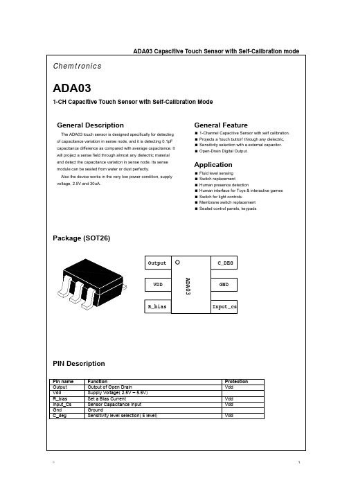
©G YWW[GjG
4
Lead Free !
ADA03 Capacitive Touch Sensor with Self-Calibration
͵ΖΔ͑͟ ͣͥ͑͑͡͡
MARKING SPECIFICATION
hU iU johyhj{lyG {wlG aG hyphsG thyrpunG tl{ovkG G a shzlyG thyrpunG shv|{G MG hylhG thG YU\G G
Characteristics Supply Voltage Current consumption Power dissipation
Symbol Vdd Idmax Pd
Test Condition
Min 2.2
Typ 120 -
Max 6.5
Units V uA
-20ଇ < Ta < +75ଇ, Vdd = 5V -20 ~ 75ଇ, Vdd = 5V
Application
Fluid level sensing Switch replacement Human presence detection Human interface for Toys & interactive games Switch for light controls. Membrane switch replacement Sealed control panels, keypads
©scinortmeh024
1
Lead Free !
ADA03 Capacitive Touch Sensor with Self-Calibration
͵ΖΔ͑͟ ͣͥ͑͑͡͡
ENC-03J中文资料(murata)中文数据手册「EasyDatasheet - 矽搜」
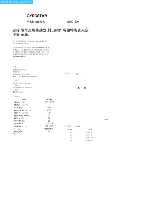
存储温度范围( C) 尺寸( mm) 重量( g最大)
All typical values.
ENCY03J W2.7 至 W5.5
5 T300 W1.35
0.67 T20 T5
50 Y5 至 W75 Y30 至 W85 15.5Z8.0Z4.3
1.0
!外部Biblioteka 尺寸MJPN
芯片中文手册,看全文,戳
GYROSTAR®
压电振动陀螺仪
ENC 系列
超小型角速度传感器,村田制作所独特陶瓷双层 振动单元.
此产品是使用科氏力,当旋转角速度被施加到振荡体时 产生现象角速度传感器.
为实现其超小体产品,超轻量,和quickresponse能力,电路已 被转换为一个定制IC除采用村田制作所独创超小型,陶瓷 双层振动单元传感器元件.检测移动物体或由于其小巧轻 便设计增加安装灵活性,当该产品提供许多优秀功能,如 quickresponse功能.
!特征 1.超小型和超轻量级 2.快速响应 3.低驱动电压;低电流消耗 4.由一个内置-AGC电路实现可靠特征
!应用 1.检测手运动涉及视频和静止
摄像头
2.在不同无振动台检测振动和
隔离
3.检测自己运动
!额定值
零件号
电源电压( VDC) 消耗电流( mA以下 .) 最大 .角速度( ˚/ s) 输出(在角速度 = 0)(伏) 比例因子( MV /˚/秒) 温度 .比例因子系数(%) 线性度(% FS)
03JA 883JPN
Sensor
DC cut
A/D
Processing
AMP
Converter
circuit
待检测每旋转轴1.一个sensot. 2.对于高精度测量,tempreature漂(在静止状态下输出波动,由于变化影响
SNA-03003035B-3XXXX Data Sheet
Asink CorporationTel:+86-755-2689 1081 Fax:+86-755-2682 6659 Product SpecificationsCustomer Name: ______________Part Name: Aluminum Foil Heat Sink Part Description: 30X30X0.35mmPart Number: SNA-03003035B-3XXXXXPREPARED BY CHECKED BY CustomerSuggestion Customer ApprovalUltra-thin,high performance productsA-sink Aluminum Foil Heat Sink is a ultera-thinHeat-sink with high thermal conductivity and highflexibility. The surface is coating with Nano Carbonpowder which has high thermal conductivity andhigh thermal radiation efficiency. Changing the heat to infrared RF, communicate cooling efficiency.Construction♦Product Cross-Sectional View ♦Products FundamentalFunctions♦Good flexibility,Rework,Processability♦EMI shielding and absorbing to protect sensitive electronic parts♦RoHS compliant and UL94V0 flammability rated♦Temperature performance>100°♦The top and bottom surfaces are insulated♦Can be die-cut into customizable shapes♦Applicable area of the phase difference♦Holds patents:our proprietary technology and know-how with competitors resolveOutline Dimension:Nano Carbon Super Thin Heat SinkPART NUMBER SNA-03003035B-3XXXXX DESCRIPTION30X30X0.35mmNano Carbon COATING ReportMain Feature Value MethodColor Black VisualAdhesion Crosscut100/100 ASTM D3359Impact test Collision-free spin-off Dupont 500g×50㎝Salt water spray test >500hr No blistering peeling ASTM B117Hardness H ASTM D3363Coating thickness 50±15μm ASTM D1186 Resistance 1.0 x 10¹²Ω ANSI/ESD STM 11.11 Accelerated weathering test >600hr UV-A340Color aberration △E≤1.0 Colorimeter Glossiness 10-15 Gloss MeterAnti-alcohol Wipe 20 times without fading Anhydrous EthanolSGS Test ReportTest Requested ValueFifteen (15) Substances of Very High Concern (SVHC) Screening Up to standard RoHS (2002/95/EC) Up to standardUp to standard DIN (EN 71 Part 3:1994 with the incorporation of amendmentsA1:2000, AC:2000 and AC:2002)ASTM F963-07(4.3.5) Up to standardNano Carbon Coating CompositionMATERIAL BalanceRESIN 60-80 ﹪FILLER/PIGMENT 10-20 ﹪ADDITIVE 10-15 ﹪FLOWAGENT 1 ﹪Conductive Adhesive Tape SpecificationItem ValueAdhesive Conductive Acrylic AdhesiveColor TransparentLiner Releasing Paper Weather resistant YesAgeing resistant YesThickness Total 0.13mm Adhesion to stainless steel(72 hour RT)142N/100 mmReliability Test ItemsNo.Test Items Test standardTest method Inspection standard Conclusion1 Salt Water Spray TestGB/T10125-1977In 35℃ for5%NaCI spray 1000 hours test No foaming, no peeling, no rustpass2Acid resistanceJIS-K-56006.1Use the 5%H2SO4solution at room temperature for 300 hours No foaming, no peeling, no rustpass3Alkali resistanceJIS-K-56006.1Use the 5%H2SO4solution at room temperature for 24 hoursNo foaming, nopeeling, no rustPass4 Boiling resistanceJIS-K-56006.3 Boiling water and cook for 1 hourNo foaming, no peeling, no rust PassNote:1. Product surface without scratches, dirt, silk, mimeographed phenomenon.2. Thermal glue stick with Aluminum foil tightly, no bubble and breakage issues.3. The product surface in 100mm only allowed less than 2 convex points appear.Packing:Precautions: Product Transportation and Storage1. The product is easy damaged on the way of transportation, it must be move carefully, don’t squeeze and press the product2. The product must be placed monolayer, don’t pile up two or more layers.3. As a result of above improper transportation and storage caused issues, we company without responsibility.。
BQ25713 BQ25713B 具有系统功率监测器和处理器热量监测器的 I2C 窄 VDC 降压
BQ25713/BQ25713B 具有系统功率监测器和处理器热量监测器的 I2C 窄 VDC 降压/升压电池充电控制器1 特性•与 BQ25703A 引脚对引脚和软件兼容•从各种输入源为 1 至 4 节电池充电–3.5V 至 24V 输入工作电压–支持 USB 2.0、USB 3.0、USB 3.1 (Type-C) 和USB 电力输送 (USB-PD) 输入电流设置–可在降压、降压/升压和升压操作之间进无缝转换–提供输入电流和电压调节(IDPM 和 VDPM)以防电源过载•用于 CPU 节流的功率/电流监控器–综合 PROCHOT 设置,符合 IMVP8/IMVP9 要求–输入和电池电流监控器–系统功率监控器,符合 IMVP8/IMVP9 要求•窄电压 DC (NVDC) 电源路径管理–即使没有电池或电池已深度放电亦可瞬时启动–适配器满载时,电池可为系统补充电量–电池 MOSFET 可在补电模式下实现理想二极管运行•通过电池给 USB 端口加电 (USB OTG)–具有 8mV 分辨率的 3V 至 20.8V VOTG–输出电流限值最高为 6.4A,且具有 50mA 分辨率•TI 获得专利的直通模式 (PTM),可提高系统功效并实现电池快速充电•当系统仅通过电池供电时,Vmin 有源保护 (VAP) 模式将会在系统峰值功率尖峰期间通过输入电容器为电池补电。
•输入电流优化器 (ICO) 可获取最大输入功率•用于 2.2µH 至 1.0µH 电感器的 800kHz 或 1.2MHz 可编程开关频率•可通过主机控制接口实现灵活系统配置–I2C 端口优化系统性能与状态报告–硬件引脚可用于设置输入电流限制,无需 EC 控制•集成型 ADC 可监控电压、电流和功率•高精度调节和监控–±0.5% 充电电压调节–±2% 输入/充电电流调节–±2% 输入/充电电流监测–±4% 功率监控器•安全–热关断–输入、系统和电池过压保护•安全相关认证:–经 IEC 62368-1 CB 认证•低电池静态电流•封装:32 引脚 4×4 WQFN2 应用•无人机、蓝牙扬声器、IP 摄像头、可拆卸电脑、平板电脑和移动电源•工业和医疗设备•带可充电电池的便携式设备3 说明此器件是一款同步 NVDC 降压/升压电池充电控制器,可为空间受限的 1-4 芯串联电池充电应用提供元件数很少的高效解决方案。
产品规格书完整
NO.:PS091101上海徕木电子股份有限公司SHANGHAI LAIMU ELECTRONICS CO., LTD.产品规格书PRODUCT SPECIFICATION顾客:Client:产品名称:Connector Product Name:产品编码:/Part Number版本号:/ Version Number:制定审核EditCheck上海市松江区洞泾镇洞薛路651弄88号徕木:Laimu:Auto Meter Connector(汽车仪表连接器)SEE TABLE/批准Approval邮编:201619上海徕木电子股份有限公司SHANGHAI LAIMU ELECTRONICS CO., LTD.编 号PS091101Serial Number 产品规格书Product Specification目版本号/ Version Number 产品名称 Connector Product Name 产品编码 See TablePart Number录CONTENT0更改记录........................................................................................................................................3 1产品描述Product description.. (4)1.1产品简图Outline drawing ..................................................................................................4 1.2产品组成BOM (5)2总体要求General (5)2.1功能描述Functional description ..........................................................................................5 2.2安装位置Mounting location ................................................................................................5 2.3温度范围Ambient temperature range .................................................................................5 2.4额定范围Rating range ........................................................................................................5 3默认测试条件Default test conditions .............................................................................................5 4产品性能Performance . (6)4.1外观Appearance..................................................................................................................6 4.2结构尺寸Dimension.............................................................................................................6 4.3接触电阻Contact resistance...................................................................................................6 4.4绝缘电阻Insulation resistance...............................................................................................6 4.5耐电压Withstand voltage......................................................................................................7 4.6温升Temperature rise............................................................................................................7 4.7插入力Connector Mating Force.............................................................................................7 4.8拔出力Connector Unmating Force.........................................................................................7 4.9端子保持力Terminal to Connector Retention...........................................................................8 4.10振动Vibration....................................................................................................................8 4.11温度循环Temperature cycling..............................................................................................8 4.12耐高温Heat Resistance.......................................................................................................9 4.13耐低温Cold Resistance.......................................................................................................9 4.14盐雾Salt spray...................................................................................................................9 4.15耐焊接热Resistance to soldering heat.................................................................................10 4.16沾锡性Solderability. (10)上海徕木电子股份有限公司SHANGHAI LAIMU ELECTRONICS CO., LTD.编 号PS091101Serial Number 产品规格书Product Specification0更改记录序号 版本号 更改前描述No.: Version Description Before ModificationNumber123456版本号/ Version Number 产品名称 Connector Product Name 产品编码 See TablePart Number更改后描述 批准 日期Description After ModificationApprovalDatePage 3 of 11FOR-TS3-D08-01版本/版次:A1上海徕木电子股份有限公司SHANGHAI LAIMU ELECTRONICS CO., LTD.编 号PS091101Serial Number 产品规格书Product Specification1产品描述Product description1.1产品简图Outline drawing适用于本规格书的产品系列,如下表:P/N.料号No. No. of PIN Color A1.2产品组成BOM1.2.1接触件:黄铜,底镀镍,整体镀锡;版本号/ Version Number 产品名称 Connector Product Name 产品编码 See TablePart NumberB C D E FContact :Brass, Pure Tin plated over Nickel under plating ; 1.2.2塑料本体:PBT+GF15;Housing :PBT+GF15;2总体要求General2.1功能描述Functional description本产品主要适用于汽车仪表控制模块与线束的电力信号传输与连接。
SN03A 中文资料
特点:
低启动电流和工作电流 逐周期峰值电流限制 内置前沿消隐 内置模拟乘法器可用于功率因子校正 内置的启动计时器 带磁滞控制的低电压保护 VCC 过压保护 工作于临界导通模式 图腾柱输出控制, 带电压钳位保护。 无异音工作 目前提供 DIP8、SOP8 两种封装形式,符合 RoHS 标准
照明和背光驱Biblioteka 系列产品高功率校正因子反激式 PWM 控制器
简介:
SN03A 是一款专为照明
设计的高功率因子反激式PWM 控制器。针对开关电源设计,集 成功率因子校正、临界模式控制、 MOSFET驱动等优化设计,使系 统更完美地应用于照明领域。
应用范围:
高功率因子反激式单级开关电 源
LED 照明电源
典型应用:
昂宝绿色引擎 TM 技术 成就绿色节能时代
昂宝绿色电源芯片 造就绿色电源世界
25
2n3904 数据表.pdf说明书
General Purpose TransistorsNPN SiliconMAXIMUM RATINGSRatingSymbol Value Unit Collector–Emitter Voltage V CEO 40Vdc Collector–Base Voltage V CBO 60Vdc Emitter–Base VoltageV EBO 6.0Vdc Collector Current — Continuous I C 200mAdc Total Device Dissipation @ T A = 25°C Derate above 25°CP D 6255.0mW mW/°C Total Device Dissipation @ T C = 25°C Derate above 25°CP D 1.512Watts mW/°C Operating and Storage Junction Temperature RangeT J , T stg–55 to +150°CTHERMAL CHARACTERISTICS (1)CharacteristicSymbol Max Unit Thermal Resistance, Junction to Ambient R q JA 200°C/W Thermal Resistance, Junction to CaseR q JC83.3°C/WELECTRICAL CHARACTERISTICS (T A = 25°C unless otherwise noted)CharacteristicSymbolMinMaxUnitOFF CHARACTERISTICSCollector–Emitter Breakdown Voltage (2)(I C = 1.0 mAdc, I B = 0)V (BR)CEO 40—Vdc Collector–Base Breakdown Voltage (I C = 10 m Adc, I E = 0)V (BR)CBO 60—Vdc Emitter–Base Breakdown Voltage (I E = 10 m Adc, I C = 0)V (BR)EBO6.0—Vdc Base Cutoff Current(V CE = 30 Vdc, V EB = 3.0 Vdc)I BL —50nAdc Collector Cutoff Current(V CE = 30 Vdc, V EB = 3.0 Vdc)I CEX—50nAdc1.Indicates Data in addition to JEDEC Requirements.2.Pulse Test: Pulse Width v 300 m s; Duty Cycle v 2.0%.Preferred devices are Motorola recommended choices for future use and best overall value.Order this documentby 2N3903/DMOTOROLASEMICONDUCTOR TECHNICAL DATA2N39032N3904*Motorola Preferred DeviceCASE 29–04, STYLE 1TO–92 (TO–226AA)123*COLLECTOR32BASE1EMITTERREV 22N39032N3904ELECTRICAL CHARACTERISTICS (T A = 25°C unless otherwise noted) (Continued)CharacteristicSymbolMinMaxUnitON CHARACTERISTICSDC Current Gain (1)(I C = 0.1 mAdc, V CE = 1.0 Vdc)2N39032N3904(I C = 1.0 mAdc, V CE = 1.0 Vdc)2N39032N3904(I C = 10 mAdc, V CE = 1.0 Vdc)2N39032N3904(I C = 50 mAdc, V CE = 1.0 Vdc)2N39032N3904(I C = 100 mAdc, V CE = 1.0 Vdc)2N39032N3904h FE204035705010030601530————150300—————Collector–Emitter Saturation Voltage (1)(I C = 10 mAdc, I B = 1.0 mAdc)(I C = 50 mAdc, I B = 5.0 mAdc V CE(sat)——0.20.3VdcBase –Emitter Saturation Voltage (1)(I C = 10 mAdc, I B = 1.0 mAdc)(I C = 50 mAdc, I B = 5.0 mAdc)V BE(sat)0.65—0.850.95VdcSMALL–SIGNAL CHARACTERISTICSCurrent–Gain — Bandwidth Product(I C = 10 mAdc, V CE = 20 Vdc, f = 100 MHz)2N39032N3904f T250300——MHzOutput Capacitance(V CB = 5.0 Vdc, I E = 0, f = 1.0 MHz)C obo — 4.0pF Input Capacitance(V EB = 0.5 Vdc, I C = 0, f = 1.0 MHz)C ibo —8.0pF Input Impedance(I C = 1.0 mAdc, V CE = 10 Vdc, f = 1.0 kHz)2N39032N3904h ie1.01.08.010k ΩVoltage Feedback Ratio(I C = 1.0 mAdc, V CE = 10 Vdc, f = 1.0 kHz)2N39032N3904h re0.10.5 5.08.0X 10–4Small–Signal Current Gain(I C = 1.0 mAdc, V CE = 10 Vdc, f = 1.0 kHz)2N39032N3904h fe50100200400—Output Admittance(I C = 1.0 mAdc, V CE = 10 Vdc, f = 1.0 kHz)h oe 1.040m mhos Noise Figure(I C = 100 m Adc, V CE = 5.0 Vdc, R S = 1.0 k Ω, f = 1.0 kHz)2N39032N3904NF——6.05.0dBSWITCHING CHARACTERISTICSDelay Time (V = 3.0 Vdc, V = 0.5 Vdc,t d —35ns Rise Time (CC BE I C = 10 mAdc, I B1 = 1.0 mAdc)t r —35ns Storage Time (V CC = 3.0 Vdc, I C = 10 mAdc,2N3903I B1 = I B2 = 1.0 mAdc)2N3904t s ——175200ns Fall Timet f—50ns1.Pulse Test: Pulse Width v 300 m s; Duty Cycle v2.0%.2N39032N3904Figure 1. Delay and Rise TimeEquivalent Test Circuit Figure 2. Storage and Fall TimeEquivalent Test Circuit+3 V27510 k 1N916C S < 4 pF*+3 V27510 kC S < 4 pF*< 1 ns–0.5 V+10.9 V300 nsDUTY CYCLE = 2%< 1 ns–9.1 V ′+10.9 VDUTY CYCLE = 2%t 110 < t 1 < 500 m s * Total shunt capacitance of test jig and connectorsTYPICAL TRANSIENT CHARACTERISTICSFigure 3. Capacitance REVERSE BIAS VOLTAGE (VOLTS)2.03.05.07.0101.00.1Figure 4. Charge DataI C , COLLECTOR CURRENT (mA)50001.0V CC = 40 V I C /I B = 10Q , C H A R G E (p C )3000200010005003002007001005070 2.0 3.0 5.07.01020305070100200C A P A C I T A N C E (p F )1.02.03.0 5.07.010*******.20.30.50.7Q TQ AC iboC oboT J = 25°C T J = 125°C2N39032N3904Figure 5. Turn–On TimeI C , COLLECTOR CURRENT (mA)7010020030050050Figure 6. Rise TimeI C , COLLECTOR CURRENT (mA)T I M E (n s )1.02.03.01020705100t , R I S E T I M E (n s )Figure 7. Storage Time I C , COLLECTOR CURRENT (mA)Figure 8. Fall TimeI C , COLLECTOR CURRENT (mA)5.07.03050200103072070100200300500501.0 2.0 3.010207051005.07.03050200103072070100200300500501.0 2.0 3.010207051005.07.03050200103072070100200300500501.0 2.0 3.010207051005.07.030502001030720r t , F A L L T I M E (n s )f t , S T O R A G E T I M E (n s )s ′V CC = 40 V I C /I B = 10V CC = 40 V I B1 = I B2I C /I B = 20I C /I B = 10I C /I B = 10t r @ V CC = 3.0 Vt d @ V OB = 0 V40 V 15 V 2.0 VI C /I B = 10I C /I B = 20I C /I B = 10I C /I B = 20t ′s = t s – 1/8 t f I B1 = I B2TYPICAL AUDIO SMALL–SIGNAL CHARACTERISTICSNOISE FIGURE VARIATIONS(V CE = 5.0 Vdc, T A = 25°C, Bandwidth = 1.0 Hz)Figure 9. f, FREQUENCY (kHz)468101220.1Figure 10.R S , SOURCE RESISTANCE (k OHMS)0N F , N O I S E F I G U R E (d B )1.02.04.01020400.20.4010046810122140.11.02.04.01020400.20.4100N F , N O I S E F I G U R E (d B )f = 1.0 kHz I C = 1.0 mAI C = 0.5 mAI C = 50 m AI C = 100 m ASOURCE RESISTANCE = 200 W I C = 1.0 mASOURCE RESISTANCE = 200 W I C = 0.5 mASOURCE RESISTANCE = 500 W I C = 100 m A SOURCE RESISTANCE = 1.0 k I C = 50 m A2N39032N3904h PARAMETERS(V CE = 10 Vdc, f = 1.0 kHz, T A = 25°C)Figure 11. Current GainI C , COLLECTOR CURRENT (mA)7010020030050Figure 12. Output AdmittanceI C , COLLECTOR CURRENT (mA)h , C U R R E N T G A I Nh , O U T P U T A D M I T T A N C E ( m h o s )Figure 13. Input Impedance I C , COLLECTOR CURRENT (mA)Figure 14. Voltage Feedback RatioI C , COLLECTOR CURRENT (mA)3010050510202.03.05.07.0101.00.10.21.02.0 5.00.5100.30.5 3.00.72.05.010201.00.20.5o e h , V O L T A G E F E E D B A C K R A T I O (X 10 )r e h , I N P U T I M P E D A N C E (k O H M S )i e 0.10.21.02.0 5.0100.30.5 3.00.10.21.02.0 5.0100.30.5 3.0210.10.21.02.0 5.0100.30.5 3.0f e m –4TYPICAL STATIC CHARACTERISTICSFigure 15. DC Current GainI C , COLLECTOR CURRENT (mA)0.30.50.71.02.00.20.1h , D C C U R R E N T G A I N (N O R M A L I Z E D )0.5 2.0 3.01050700.20.30.11001.00.720030205.07.0F E V CE = 1.0 VT J = +125°C+25°C–55°C2N39032N3904Figure 16. Collector Saturation RegionI B , BASE CURRENT (mA)0.40.60.81.00.20.1V , C O L L E C T O R E M I T T E R V O L T A G E (V O L T S )0.5 2.0 3.0100.20.301.00.7 5.07.0CE I C = 1.0 mAT J = 25°C0.070.050.030.020.0110 mA30 mA100 mAFigure 17. “ON” Voltages I C , COLLECTOR CURRENT (mA)0.40.60.81.01.20.2Figure 18. Temperature CoefficientsI C , COLLECTOR CURRENT (mA)V , V O L T A G E (V O L T S )1.02.0 5.01020500100–0.500.51.0060801201401601802040100C O E F F I C I E N T (m V / C )200–1.0–1.5–2.0200°T J = 25°C V BE(sat) @ I C /I B =10V CE(sat) @ I C /I B =10V BE @ V CE =1.0 V+25°C TO +125°C–55°C TO +25°C +25°C TO +125°C–55°C TO +25°Cq VC FOR V CE(sat)q VB FOR V BE(sat)2N39032N3904PACKAGE DIMENSIONSNOTES:1.DIMENSIONING AND TOLERANCING PER ANSI Y14.5M, 1982.2.CONTROLLING DIMENSION: INCH.3.CONTOUR OF PACKAGE BEYOND DIMENSION R IS UNCONTROLLED.4.DIMENSION F APPLIES BETWEEN P AND L.DIMENSION D AND J APPLY BETWEEN L AND K MINIMUM. LEAD DIMENSION IS UNCONTROLLED IN P AND BEYOND DIMENSION K MINIMUM.RAPJL FBKGH SECTION X–XC VDNNX XSEATINGPLANEDIM MIN MAX MIN MAX MILLIMETERSINCHES A 0.1750.205 4.45 5.20B 0.1700.210 4.32 5.33C 0.1250.165 3.18 4.19D 0.0160.0220.410.55F 0.0160.0190.410.48G 0.0450.055 1.15 1.39H 0.0950.105 2.42 2.66J 0.0150.0200.390.50K 0.500–––12.70–––L 0.250––– 6.35–––N 0.0800.105 2.04 2.66P –––0.100––– 2.54R 0.115––– 2.93–––V0.135–––3.43–––1STYLE 1:PIN 1.EMITTER2.BASE3.COLLECTORCASE 029–04(TO–226AA)ISSUE AD2N39032N3904Motorola reserves the right to make changes without further notice to any products herein. Motorola makes no warranty, representation or guarantee regarding the suitability of its products for any particular purpose, nor does Motorola assume any liability arising out of the application or use of any product or circuit, and specifically disclaims any and all liability, including without limitation consequential or incidental damages. “Typical” parameters which may be provided in Motorola data sheets and/or specifications can and do vary in different applications and actual performance may vary over time. All operating parameters, including “Typicals”must be validated for each customer application by customer’s technical experts. Motorola does not convey any license under its patent rights nor the rights of others. Motorola products are not designed, intended, or authorized for use as components in systems intended for surgical implant into the body, or other applications intended to support or sustain life, or for any other application in which the failure of the Motorola product could create a situation where personal injury or death may occur. Should Buyer purchase or use Motorola products for any such unintended or unauthorized application, Buyer shall indemnify and hold Motorola and its officers, employees, subsidiaries, affiliates, and distributors harmless against all claims, costs, damages, and expenses, and reasonable attorney fees arising out of, directly or indirectly, any claim of personal injury or death associated with such unintended or unauthorized use, even if such claim alleges that Motorola was negligent regarding the design or manufacture of the part. Motorola and are registered trademarks of Motorola, Inc. Motorola, Inc. is an Equal Opportunity/Affirmative Action Employer.How to reach us:USA/EUROPE/Locations Not Listed: Motorola Literature Distribution;JAPAN: Nippon Motorola Ltd.; T atsumi–SPD–JLDC, 6F Seibu–Butsuryu–Center, P.O. Box 5405; Denver, Colorado 80217. 1–800–441–24473–14–2 T atsumi Koto–Ku, T okyo 135, Japan. 81–3–3521–8315MFAX: RMFAX0@ – TOUCHTONE 602–244–6609ASIA/PACIFIC: Motorola Semiconductors H.K. Ltd.; 8B T ai Ping Industrial Park, INTERNET: http://Design–51 Ting Kok Road, T ai Po, N.T., Hong Kong. 852–26629298。
CR03Adatasheet
C
IGT (µA)
1 ~ 30
20 ~ 50
40 ~ 100
The above values do not include the current flowing through the 1kΩ resistance between the gate and cathode.
Limits Typ. — — — — — — 1.5 —
8 6 4 2 0 100 2 3 4 5 7 101 2 3 4 5 7 102
CONDUCTION TIME (CYCLES AT 60Hz)
Feb.1999
MITSUBISHI SEMICONDUCTOR 〈THYRISTOR〉
CR03AM
LOW POWER USE NON-INSULATED TYPE, GLASS PASSIVATION TYPE
12.5 MIN
2
3 1
VOLTAGE CLASS
TYPE NAME
1 T1 TERMINAL 2 T2 TERMINAL 3 GATE TERMINAL
CIRCUMSCRIBE CIRCLE φ0.7
1.25 1.25
1.3 3.9 MAX
• IT (AV) ........................................................................ 0.3A • VDRM ..............................................................400V/600V • IGT ......................................................................... 100µA
MBRA140T3G;MBRA140T3;中文规格书,Datasheet资料
Figure 5. Current Derating
R (T) , TRANSIENT THERMAL RESISTANCE (NORMALIZED) T, TIME (s) 1.0E+0
Figure 6. Forward Power Dissipation
中文规格书datasheet资料datasheetdatasheet网站l298ndatasheeticdatasheetpl2303datasheetds18b20datasheetdatasheetcomlm324datasheetrt5350datasheet
MBRA140T3G, NRVBA140T3G Surface Mount Schottky Power Rectifier
vF, INSTANTANEOUS FORWARD VOLTAGE (VOLTS)
Figure 1. Typical Forward Voltage
Figure 2. Maximum Forward Voltage
100E-3 I R , REVERSE CURRENT (AMPS)
100E-3 I R , MAXIMUM REVERSE CURRENT (AMPS)
†For information on tape and reel specifications, including part orientation and tape sizes, please refer to our Tape and Reel Packaging Specifications Brochure, BRD8011/D.
10E-3
TJ = 125C TJ = 85C
10E-3 TJ = 85C 1.0E-3 TJ = 25C
预防安全自动化产品数据册-XPSUAT13A3AP预防模块说明书
T h e i n f o r m a t i o n p r o v i d e d i n t h i s d o c u m e n t a t i o n c o n t a i n s g e n e r a l d e s c r i p t i o n s a n d /o r t e c h n i c a l c h a r a c t e r i s t i c s o f t h e p e r f o r m a n c e o f t h e p r o d u c t s c o n t a i n e d h e r e i n .T h i s d o c u m e n t a t i o n i s n o t i n t e n d e d a s a s u b s t i t u t e f o r a n d i s n o t t o b e u s e d f o r d e t e r m i n i n g s u i t a b i l i t y o r r e l i a b i l i t y o f t h e s e p r o d u c t s f o r s p e c i f i c u s e r a p p l i c a t i o n s .I t i s t h e d u t y o f a n y s u c h u s e r o r i n t e g r a t o r t o p e r f o r m t h e a p p r o p r i a t e a n d c o m p l e t e r i s k a n a l y s i s , e v a l u a t i o n a n d t e s t i n g o f t h e p r o d u c t s w i t h r e s p e c t t o t h e r e l e v a n t s p e c i f i c a p p l i c a t i o n o r u s e t h e r e o f .N e i t h e r S c h n e i d e r E l e c t r i c I n d u s t r i e s S A S n o r a n y o f i t s a f f i l i a t e s o r s u b s i d i a r i e s s h a l l b e r e s p o n s i b l e o r l i a b l e f o r m i s u s e o f t h e i n f o r m a t i o n c o n t a i n e d h e r e i n .Product data sheetCharacteristicsXPSUAT13A3APPreventa module Cat.4 features XPSUAK +delayed outputs 24vac/dc screwMainRange of product Preventa Safety automation Product or component typePreventa safety module Safety module name XPSUATSafety module applicationMonitoring antivalent contactsFor emergency stop, guard and light curtain monitoringMonitoring of pressure-sensitive 4-wire protective devicesFunction of moduleEmergency stop button with 2 NC contacts Guard monitoring with 1 or 2 limit switches Monitoring 2 PNP sensors Magnetic switch monitoring Light curtain monitoring RFID switchMonitoring of electro-sensitive protection equipment (ESPE)Sensing mat/edgesProximity sensor monitoringMonitoring 1 PNP + 1 NPN sensorSafety levelCan reach PL e/category 4 for normally open relay contact ISO 13849-1Can reach SILCL 3 for normally open relay contact IEC 62061Can reach SIL 3 for normally open relay contact IEC 61508Can reach PL c/category 1 for normally closed relay contact ISO 13849-1Can reach SILCL 1 for normally closed relay contact IEC 62061Can reach SIL 1 for normally closed relay contact IEC 61508Safety reliability dataMTTFd > 30 years ISO 13849-1Dcavg >= 99 % ISO 13849-1PFHd = 0.94E-09 for SS0 ISO 13849-1PFHd = 0.95E-09 for SS1 ISO 13849-1HFT = 1 IEC 62061PFHd = 0.94E-09 for SS0 IEC 62061PFHd = 0.95E-09 for SS1 IEC 62061SFF > 99% IEC 62061HFT = 1 IEC 61508-1PFHd = 0.94E-09 for SS0 IEC 61508-1PFHd = 0.95E-09 for SS1 IEC 61508-1SFF > 99% IEC 61508-1Type = B IEC 61508-1Electrical circuit typeNC pair PNP pairAntivalent pair OSSD pairConnections - terminalsRemovable screw terminal block, 0.2...2.5 mm² solid or flexibleRemovable screw terminal block, 0.25...2.5 mm²flexible with ferrule single conductorRemovable screw terminal block, 0.2...1.5 mm² solid or flexible twin conductorRemovable screw terminal block, 2 x 0.25...1 mm²flexible with ferrule without cable end, with bezel Removable screw terminal block, 2 x 0.5...1.5 mm²flexible with ferrule with cable end, with bezel [Us] rated supply voltage24 V AC - 15...10 %24 V DC - 20...20 %ComplementarySynchronisation time between inputs0.5 s2 s4 sType of start Automatic/manual/monitoredPower consumption in W3 W 24 V DCPower consumption in VA 6.5 VA 24 V AC 50/60 HzInput protection type Internal, electronicSafety outputs 1 NC3 NO3 NOSafety inputs21Maximum wire resistance500 OhmTime delay range0...900 sInput compatibility Normally closed circuit ISO 14119XC limit switch ISO 14119Mechanical contact ISO 14119Normally closed circuit ISO 13850Antivalent pair ISO 14119OSSD pair IEC 61496-1-23-wire proximity sensors PNPOutput type Relay output, 250 V ACRelay output, 250 V ACRelay output, 24 V DCRelay output, 24 V DC[Ie] rated operational current5 A AC-13 A AC-155 A DC-13 A DC-133 A AC-11 A AC-153 A DC-11 A DC-13Control outputs 4 pulsed outputInput/output type Semiconductor output Z2, 20 mAPulsed output for diagnostics Z1, 20 mA [Ith] conventional free air thermal current16 AAssociated fuse rating10 A gG NO relay output circuit IEC 60947-1 Minimum output current20 mA relay outputMinimum output voltage24 V relay outputMaximum response time on input open20 ms[Ui] rated insulation voltage250 V 2)EN/IEC 60947-1[Uimp] rated impulse withstand voltage4 kV II EN/IEC 60947-1Local signalling Power ON LED green)Error LED red)Start LED yellow)Safety output instantaneous LED yellow)Safety output delayed LED yellow)Safety input S12 LED yellow)Safety input S22 LED yellow)Safety input S32 LED yellow)Mounting support35 mm symmetrical DIN railMaximum Depth 4.72 in (120 mm)Maximum Height 3.94 in (100 mm)Maximum Width 1.77 in (45 mm)Net Weight0.77 lb(US) (0.350 kg)EnvironmentStandards IEC 60947-5-1IEC 61508-1 functional safety standardIEC 61508-2 functional safety standardIEC 61508-3 functional safety standardIEC 61508-4 functional safety standardIEC 61508-5 functional safety standardIEC 61508-6 functional safety standardIEC 61508-7 functional safety standardISO 13849-1 functional safety standardIEC 62061 functional safety standardProduct certifications TÜVCULusIP degree of protection IP54 mounting area)EN/IEC 60947-1IP40 housing)EN/IEC 60947-1IP20 terminals)EN/IEC 60947-1Ambient air temperature for storage-13…185 °F (-25…85 °C)Relative humidity5…95 % non-condensingOrdering and shipping detailsNbr. of units in pkg.1Package weight(Lbs)15.34 oz (435 g)Packing UnitsUnit Type of Package 1PCEPackage 1 Height 2.56 in (6.5 cm)Package 1 width 5.31 in (13.5 cm)Package 1 Length 6.10 in (15.5 cm)Unit Type of Package 2BB1Number of Units in Package 21Package 2 Weight16.23 oz (460 g)Package 2 Height 2.52 in (6.4 cm)Package 2 width 5.24 in (13.3 cm)Package 2 Length 6.02 in (15.3 cm)Unit Type of Package 3S03Number of Units in Package 316Package 3 Weight17.13 lb(US) (7.77 kg)Package 3 Height11.81 in (30 cm)Package 3 width11.81 in (30 cm)Package 3 Length15.75 in (40 cm)Offer SustainabilitySustainable offer status Green Premium productEU RoHS Directive Pro-active compliance (Product out of EU RoHS legal scope)EU RoHSDeclarationMercury free YesRoHS exemption information YesChina RoHS Regulation China RoHS DeclarationEnvironmental Disclosure Product Environmental ProfileCircularity Profile End Of Life InformationWEEE The product must be disposed on European Union markets following specificwaste collection and never end up in rubbish bins.PVC free YesDimensions DrawingsDimensionsFront and Side Views(A) :Product drawing(B) :Screw clamp terminal (C) :Side view(1) :Removable terminal blocks, top (2) :Removable terminal blocks, bottom (3) :LED indicators(4) :Start function selector (5) :Function selector (6) :Delay factor selector (7) :Delay base selector(8) :Connector for optional output extension module (lateral)(9) :Sealable transparent coverMounting and Clearance Mounting to DIN railScrew-mountingConnections and SchemaWiring Drawing(1) :A1-A2 (Power supply)(2) :S11-S12-S21-S22-S31-S32 (Single-channel safety input)(3) :Y1-Y2 (Start)13-23-33-47-57-67-75-14-24-34-48-58-68-76 :OutputEXT :Connector for optional extension module B2 :Common ground terminalZ1 :Pulsed output for diagnostics, not safety-related Z2 :Solid state output, not safety-related。
SN03A 昂宝
SN03A offers great protection coverage including
o system VCC under voltage lockout (UVLO),VCC t over voltage protection, Cycle-by-cycle current
limiting, and gate drive output clamping for
Cl=1000pF, 10~90%
Bright
On
©On-Bright Electronics
Confidential -2-
Preliminary Datasheet OB_DOC_DS_SN03A00
Marking Information
SN03A
High Power Factor Flyback PWM Controller
Confidentia TYPICAL APPLICATION
Bright
On
©On-Bright Electronics
Confidential -1-
Preliminary Datasheet OB_DOC_DS_SN03A00
SN03A
High Power Factor Flyback PWM Controller
SN03A
High Power Factor Flyback PWM Controller
Product Specification
GENERAL DESCRIPTION
FEATURES
• Low Start-up Current and Operating Current
SN03A is a high power factor flyback PWM controller special for lighting applications.
BYQ30E-200 Dual ultrafast power diode datasheet说明书
BYQ30E-200Dual ultrafast power diodeRev.05 - 5 June 2018Product data sheet1. General descriptionDual ultrafast power diode in a SOT78 (TO-220AB) plastic package.2. Features and benefits• Fast switching• Low thermal resistance• High thermal cycling performance• Low forward voltage drop• Reverse surge capability• Soft recovery characteristic3. Applications• Output rectifiers in high-frequency switched-mode power supplies4. Quick reference data5. Pinning information6. Ordering information7. Marking8. Limiting values Table 5. Limiting values9. Thermal characteristics10. Characteristics11. Package outline12. Revision history13. Legal informationData sheet status[1lease consult the most recently issued document before initiating or completing a design.[2]The term 'short data sheet' is explained in section "Definitions".[3]The product status of device(s) described in this document may havechanged since this document was published and may differ in case ofmultiple devices. The latest product status information is available onthe Internet at URL h ttp://.DefinitionsDraft — The document is a draft version only. The content is still under internal review and subject to formal approval, which may result in modifications or additions. WeEn Semiconductors does not give any representations or warranties as to the accuracy or completeness of information included herein and shall have no liability for the consequences of use of such information.Short data sheet — A short data sheet is an extract from a full data sheet with the same product type number(s) and title. A short data sheet is intended for quick reference only and should not be relied upon to contai n detailed and full information. For detailed and full information see the relevant full data sheet, which is available on request via the local WeE n Semiconductors sales office. In case of any inconsistency or conflict with the short data sheet, the full data sheet shall prevail.Product specification — The information and data provided in a Product data sheet shall define the specification of the product as agreed between WeEn Semiconductors and its customer, unless WeEn Semiconductors and customer have explicitly agreed otherwise in writing. In no event however, shall an agreement be valid in which the WeEn Semiconductors productis deemed to offer functions and qualities beyond those described in the Product data sheet.DisclaimersLimited warranty and liability — Information in this document is believedto be accurate and reliable. However, WeEn Semiconductors does notgive any representations or warranties, expressed or implied, as to the accuracy or completeness of such information and shall have no liability for the consequences of use of such information. WeEn Semiconductors takes no responsibility for the content in this document if provided by an information source outside of WeEn Semiconductors.In no event shall WeEn Semiconductors be liable for any indirect, incidental, punitive, special or consequential damages (including - without limitation -lost profits, lost savings, business interruption, costs related to the removal or replacement of any products or rework charges) whether or not such damages are based on tort (including negligence), warranty, breach of contract or any other legal theory.Notwithstanding any damages that customer might incur for any reason whatsoever, WeEn Semiconductors’ aggregate and cumulative liabilit y towards customer for the products described herein shall be limited in accordance with the Terms and conditions of commercial sale of WeEn Semiconductors.Right to make changes — WeEn Semiconductors reserves the right t o make changes to information published in this document, including without limitation specifications and product descriptions, at any time and without notice. This document supersedes and replaces all information supplied prior to the publication hereof.Suitability for use — WeEn Semiconductors products are not designed, authorized or warranted to be suitable for use in life support, life-criticalor safety-critical systems or equipment, nor in applications where failureor malfunction of an WeEn Semiconductors product can reasonabl ybe expected to result in personal injury, death or severe property o r environmental damage. WeEn Semiconductors and its suppliers accept n o liability for inclusion and/or use of WeEn Semiconductors products in such equipment or applications and therefore such inclusion and/or use is at th e customer’s own risk.Quick reference data — The Quick reference data is an extract of th e product data given in the Limiting values and Characteristics sections of this document, and as such is not complete, exhaustive or legally binding. Applications — Applications that are described herein for any of these products are for illustrative purposes only. WeEn Semiconductors makesno representation or warranty that such applications will be suitable for the specified use without further testing or modification.Customers are responsible for the design and operation of their applications and products using WeEn Semiconductors products, and WeEn Semiconductors accepts no liability for any assistance with applications or customer product design. It is customer’s sole responsibility to determine whether the WeEn Semiconductors product is suitable and fit for the customer’s applications and products planned, as well as for the planned application and use of customer’s third party customer(s). Customers shoul d provide appropriate design and operating safeguards to minimize the risks associated with their applications and products.WeEn Semiconductors does not accept any liability related to any default, damage, costs or problem which is based on any weakness or defaultin the customer’s applications or products, or the application or use by customer’s third party customer(s). Customer is responsible for doing al l necessary testing for the customer’s applications and products using WeEn Semiconductors products in order to avoid a default of the applicationsand the products or of the application or use by customer’s third party customer(s). WeEn does not accept any liability in this respect.Limiting values — Stress above one or more limiting values (as defined in the Absolute Maximum Ratings System of IEC 60134) will cause permanent damage to the device. Limiting values are stress ratings only and (proper) operation of the device at these or any other conditions above thosegiven in the Recommended operating conditions section (if present) or the Characteristics sections of this document is not warranted. Constant o r repeated exposure to limiting values will permanently and irreversibly affect the quality and reliability of the device.No offer to sell or license — Nothing in this document may be interprete d or construed as an offer to sell products that is open for acceptance or the grant, conveyance or implication of any license under any copyrights, patents or other industrial or intellectual property rights.Export control — This document as well as the item(s) described herein may be subject to export control regulations. Export might require a prior authorization from competent authorities.Non-automotive qualified products — Unless this data sheet expressl y states that this specific WeEn Semiconductors product is automotiv e qualified, the product is not suitable for automotive use. It is neither qualifie d nor tested in accordance with automotive testing or application requirements. WeEn Semiconductors accepts no liability for inclusion and/or use of non-automotive qualified products in automotive equipment or applications.In the event that customer uses the product for design-in and use in automotive applications to automotive specifications and standards, customer (a) shall use the product without WeEn Semiconductors’ warrant y of the product for such automotive applications, use and specifications, and (b) whenever customer uses the product for automotive applications beyond WeEn Semiconductors’ specifications such use shall be solely at customer’s own risk, and (c) customer fully indemnifies WeEn Semiconductors fo rany liability, damages or failed product claims resulting from customer design and use of the product for automotive applications beyond WeEn Semiconductors’ standard warranty and WeEn Semiconductors’ product specifications.]PTranslations — A non-English (translated) version of a document is for reference only. The English version shall prevail in case of any discrepancy between the translated and English versions.TrademarksNotice: All referenced brands, product names, service names and trademarks are the property of their respective owners.WeEn Semiconductors BYQ30E-200Dual ultrafast power diodeBYQ30E-200Product data sheet All information provided in this document is subject to legal disclaimers.© WeEn Semiconductors Co.,Ltd.2018.All rights reserved5 June 201811 / 1114. Contents1. General description (1)2. Features and benefits (1)3. Applications (1)4. Quick reference data (1)5. Pinning information (2)6. Ordering information (2)7. Marking (2)8. Limiting values (3)9. Thermal characteristics (4)10. Characteristics (5)11. Package outline (7)12. Revision history (8)13. Legal information (9)14. Contents (11)© WeEn Semiconductors Co., Ltd. 2018. All rights reservedFor more information, please visit: Forsalesofficeaddresses,pleasesendanemailto:**************************** Date of release: 5 June 2018。
SN03A高功率因素反激式脉宽调制控制器
SN03A高功率因素反激式脉宽调制控制器总体描述SN03A 是一个专用于照明应用的高功率因数反激式脉宽调制控制器。
SN03A具有内部计时器启动的独立应用,一个功率因素校正模拟乘法器,临界模式零电流检测器,一个内置前沿消隐的检测电流比较器和一个图腾柱输出驱动功率场效应管。
SN03A提供多种保护,包括VCC电压欠压锁定,VCC过压保护,逐周电流限制和栅极驱动输出钳位对外部功率场效应管的保护。
主要特点●低启动电流和工作电流●逐周电流限制●内置前沿消隐●功率因素校正模拟乘法器●精度为1.5%的内部带隙参考●带滞环的欠电压闭锁●Vcc电压过电压保护●临界工作模式●图腾柱输出钳位●无音频噪声应用领域●单级高功率因素的反激式交流/直流开关电源●照明电源典型应用电路引脚定义、额定值及订购信息产品本体信息Y:年份代码 Y:年份代码WW:星期代码(01-52) WW:星期代码(01-52)ZZZ:批次码 ZZZ:批次码C: SOP8封装 A:DIP8封装P:无铅封装 P:无铅封装S:内部代码(可选的) S:内部代码(可选的)引脚描述引脚数 引脚功能名称 输入/输出 引脚功能描述1反馈脚 输入 误差放大器输入端2补偿脚 输出 误差放大器输出端。
一个反馈网络被放在反馈脚和补偿脚之间。
补偿脚和电流感应引脚 4产生脉宽调制占空比.3乘法器 输入 输入乘法器。
此脚通过一个电阻分压器接到整流桥输出电压从而给电流环提供一个正弦参考电压。
4电流感应引脚 输入 电流感应输入引脚。
连接到场效应管电流感应节点。
5零电流检测脚 输入 零电流检测输入。
激活时,一个新的开关周期开始。
6接地脚 电源 接地引脚7栅极驱动脚 输出 栅极驱动输出。
驱动场效应管。
8电源电压 电源 IC内部直流供电电压内部方框图工作描述SN03A 是一个专用于照明应用的高功率因数反激式脉宽调制控制器。
这种过渡模式控制大大减少了开关导通损耗,提高转换效率,并且提供非常良好的功率因素校正。
- 1、下载文档前请自行甄别文档内容的完整性,平台不提供额外的编辑、内容补充、找答案等附加服务。
- 2、"仅部分预览"的文档,不可在线预览部分如存在完整性等问题,可反馈申请退款(可完整预览的文档不适用该条件!)。
- 3、如文档侵犯您的权益,请联系客服反馈,我们会尽快为您处理(人工客服工作时间:9:00-18:30)。
f
n
o
c
n
O
d
i
n
o
c
t
h
O
i
r
m
r
a
h
c
o
t
O
m
r
l
a
i
t
n
c
h
g
i
r
B
n
O
O
n
O
O n
-B
r i
g h
c o Analog Multiplier for Power Factor
Correction
The built-in analog multiplier output limits the
MOSFET peak current with respect to the AC half
wave rectified input voltage. Through controlling
the CS comparator threshold as the AC line
voltage traverses sinusoidally from zero to peak
line voltage, the load appears to be resistive to the
AC line and near to unity power factor can be
achieved. In SN03A, the two inputs for the
multiplier are designed to achieve good linearity
n
O
O n
t
c o n f
i d
e n
t i a
l t o c h a r m r i c
Dimensions In Millimeters Dimensions In Inches Symbol
Min Max Min Max
A 1.350 1.750 0.053 0.069 A1 0.050 0.250 0.002 0.010 A2 1.250 1.650 0.049 0.065 b 0.310 0.510 0.012 0.020
O n
-B
r i
g h
t
c o n f
i d
e n
t i a
l t o c h a r m r i c h
IMPORTANT NOTICE
RIGHT TO MAKE CHANGES
On-Bright Electronics Corp. reserves the right to make corrections, modifications, enhancements, improvements and other changes to its products and services at any time and to discontinue any product or service without notice. Customers should obtain the latest relevant information before placing orders and should verify that such information is current and complete.
WARRANTY INFORMATION
On-Bright Electronics Corp. warrants performance of its hardware products to the specifications applicable at the time of sale in accordance with its standard warranty. Testing and other quality control techniques are used to the extent it deems necessary to support this warranty. Except where mandated by government requirements, testing of all parameters of each product is not necessarily performed.
On-Bright Electronics Corp. assumes no liability for application assistance or customer product design. Customers are responsible for their products and applications using On-Bright’s components, data sheet and application notes. To minimize the risks associated with customer products and applications, customers should provide adequate design and operating safeguards.
LIFE SUPPORT
On-Bright Electronics Corp.’s products are not designed to be used as components in devices intended to support or sustain human life. On-bright Electronics Corp. will not be held liable for any damages or claims resulting from the use of its products in medical applications.
MILITARY
On-Bright Electronics Corp.’s products are not designed for use in military applications. On-Bright Electronics Corp. will not be held liable for any damages or claims resulting from the use of its products in military applications.。