MT48LC4M32B2中文数据手册
MEMORY存储芯片MT48LC4M32B2TG-7 G中文规格书

Table 31: MPR Readout Serial Format (Continued)MPR Readout Parallel FormatParallel format implies that the MPR data is returned in the first data UI and then repea-ted in the remaining UIs of the burst, as shown in the table below. Data pattern location0 is the only location used for the parallel format. RD/RDA from data pattern locations1, 2, and 3 are not allowed with parallel data return mode. In this example, the patternprogrammed in the data pattern location 0 is 0111 1111. The x4 configuration only out-puts the first four bits (0111 in this example). For the x16 configuration, the same pat-tern is repeated on both the upper and lower bytes.Table 32: MPR Readout – Parallel Format4Gb: x4, x8, x16 DDR4 SDRAM Multipurpose RegisterTable 84: Command and Address Input Levels: DDR4-1600 Through DDR4-2400 (Continued)Notes: 1.For input except RESET_n. V REF = V REFCA(DC).2.V REF = V REFCA(DC).3.Input signal must meet V IL /V IH(AC) to meet t IS timings and V IL /V IH(DC) to meet t IH timings.4.The AC peak noise on V REF may not allow V REF to deviate from V REFCA(DC) by more than±1% V DD (for reference: approximately ±12mV).5.Refer to “Overshoot and Undershoot Specifications.”Table 85: Command and Address Input Levels: DDR4-2666Notes: 1.For input except RESET_n. V REF = V REFCA(DC).2.V REF = V REFCA(DC).3.Input signal must meet V IL /V IH(AC) to meet t IS timings and V IL /V IH(DC) to meet t IH timings.4.The AC peak noise on V REF may not allow V REF to deviate from V REFCA(DC) by more than±1% V DD (for reference: approximately ±12mV).5.Refer to “Overshoot and Undershoot Specifications.”Table 86: Command and Address Input Levels: DDR4-2933 and DDR4-3200Notes: 1.For input except RESET_n. V REF = V REFCA(DC).2.V REF = V REFCA(DC).3.Input signal must meet V IL /V IH(AC) to meet t IS timings and V IL /V IH(DC) to meet t IH timings.4.The AC peak noise on V REF may not allow V REF to deviate from V REFCA(DC) by more than±1% V DD (for reference: approximately ±12mV).5.Refer to “Overshoot and Undershoot Specifications.”4Gb: x4, x8, x16 DDR4 SDRAM Electrical Characteristics – AC and DC Single-Ended Input Measurement Levels。
MEMORY存储芯片MT48LC8M32LFB5-8IT中文规格书

When write leveling is enabled, the rising edge of DQS samples CK, and the prime DQoutputs the sampled CK’s status. The prime DQ for a x4 or x8 configuration is DQ0 withall other DQ (DQ[7:1]) driving LOW. The prime DQ for a x16 configuration is DQ0 for thelower byte and DQ8 for the upper byte. It outputs the status of CK sampled by LDQSand UDQS. All other DQ (DQ[7:1], DQ[15:9]) continue to drive LOW. Two prime DQ on ax16 enable each byte lane to be leveled independently.The write leveling mode register interacts with other mode registers to correctly config-ure the write leveling functionality. Besides using MR1[7] to disable/enable write level-ing, MR1[12] must be used to enable/disable the output buffers. The ODT value, burstlength, and so forth need to be selected as well. This interaction is shown in Table 71. Itshould also be noted that when the outputs are enabled during write leveling mode, theDQS buffers are set as inputs, and the DQ are set as outputs. Additionally, during writeleveling mode, only the DQS strobe terminations are activated and deactivated via theODT ball. The DQ remain disabled and are not affected by the ODT ball.Table 71: Write Leveling MatrixNotes: 1.Expected usage if used during write leveling: Case 1 may be used when DRAM are on adual-rank module and on the rank not being leveled or on any rank of a module notbeing leveled on a multislot system. Case 2 may be used when DRAM are on any rank ofa module not being leveled on a multislot system. Case 3 is generally not used. Case 4 isgenerally used when DRAM are on the rank that is being leveled.2.Since the DRAM DQS is not being driven (MR1[12] = 1), DQS ignores the input strobe,and all R TT,nom values are allowed. This simulates a normal standby state to DQS.3.Since the DRAM DQS is being driven (MR1[12] = 0), DQS captures the input strobe, andonly some R TT,nom values are allowed. This simulates a normal write state to DQS.Figure 53: READ Latency (AL = 5, CL = 6)CKCK#CommandDQDQS, DQS#BC4Address busNote: 1.MR2[18, 15:11, 8, and 2:0] are reserved for future use and must all be programmed to 0.CAS WRITE Latency (CWL)CWL is defined by MR2[5:3] and is the delay, in clock cycles, from the releasing of the internal write to the latching of the first data in. CWL must be correctly set to the corre-sponding operating clock frequency (see Figure 54 (page 136)). The overall WRITE la-tency (WL) is equal to CWL + AL (Figure 52 (page 132)).Figure 55: CAS WRITE LatencyCKCK#CommandDQDQS, DQS#Don’t CareIndicates break in time scaleTransitioning Data AUTO SELF REFRESH (ASR)Mode register MR2[6] is used to disable/enable the ASR function. When ASR is disabled,the self refresh mode’s refresh rate is assumed to be at the normal 85°C limit (some-times referred to as 1x refresh rate). In the disabled mode, ASR requires the user to en-and t RP is met). When the MPR is enabled, any subsequent READ or RDAP commandsare redirected to the multipurpose register. The resulting operation when either a READor a RDAP command is issued, is defined by MR3[1:0] when the MPR is enabled (seeTable 74 (page 140)). When the MPR is enabled, only READ or RDAP commands are al-lowed until a subsequent MRS command is issued with the MPR disabled (MR3[2] = 0).Power-down mode, self refresh, and any other nonREAD/RDAP commands are not al-lowed during MPR enable mode. The RESET function is supported during MPR enablemode.Figure 57: Multipurpose Register (MPR) Block DiagramNotes: 1. A predefined data pattern can be read out of the MPR with an external READ com-mand.2.MR3[2] defines whether the data flow comes from the memory core or the MPR. Whenthe data flow is defined, the MPR contents can be read out continuously with a regularREAD or RDAP command.Table 73: MPR Functional Description of MR3 BitsMPR Functional DescriptionThe MPR JEDEC definition enables either a prime DQ (DQ0 on a x4 and a x8; on a x16,DQ0 = lower byte and DQ8 = upper byte) to output the MPR data with the remainingDQs driven LOW, or for all DQs to output the MPR data . The MPR readout supportsfixed READ burst and READ burst chop (MRS and OTF via A12/BC#) with regular READlatencies and AC timings applicable, provided the DLL is locked as required.ZQ CALIBRATION OperationThe ZQ CALIBRATION command is used to calibrate the DRAM output drivers (R ON )and ODT values (R TT ) over process, voltage, and temperature, provided a dedicated 240Ω (±1%) external resistor is connected from the DRAM’s ZQ ball to V SSQ .DDR3 SDRAM require a longer time to calibrate R ON and ODT at power-up initialization and self refresh exit, and a relatively shorter time to perform periodic calibrations.DDR3 SDRAM defines two ZQ CALIBRATION commands: ZQCL and ZQCS. An example of ZQ calibration timing is shown below.All banks must be precharged and t RP must be met before ZQCL or ZQCS commands can be issued to the DRAM. No other activities (other than issuing another ZQCL or ZQCS command) can be performed on the DRAM channel by the controller for the du-ration of t ZQinit or t ZQoper. The quiet time on the DRAM channel helps accurately cali-brate R ON and ODT. After DRAM calibration is achieved, the DRAM should disable the ZQ ball’s current consumption path to reduce power.ZQ CALIBRATION commands can be issued in parallel to DLL RESET and locking time.Upon self refresh exit, an explicit ZQCL is required if ZQ calibration is desired.In dual-rank systems that share the ZQ resistor between devices, the controller must not enable overlap of t ZQinit, t ZQoper, or t ZQCS between ranks.Figure 62: ZQ CALIBRATION Timing (ZQCL and ZQCS)Command Indicates break in time scaleT0T1Ta0Ta1Ta2Ta3Tb0Tb1Tc0Tc1Tc2AddressA10CKCK#Don’t CareDQODT CKE Notes:1.CKE must be continuously registered HIGH during the calibration procedure.2.ODT must be disabled via the ODT signal or the MRS during the calibration procedure.3.All devices connected to the DQ bus should be High-Z during calibration.。
MEMORY存储芯片MT48LC16M16A2B4-6A IT G中文规格书

PRECHARGEThe PRECHARGE command is used to deactivate the open row in a particular bank or the open row in all banks. The bank(s) will be available for a subsequent row activation a specified time (t RP) after the PRECHARGE command is issued, except in the case of concurrent auto precharge, where a READ or WRITE command to a different bank is al-lowed as long as it does not interrupt the data transfer in the current bank and does not violate any other timing parameters. After a bank has been precharged, it is in the idle state and must be activated prior to any READ or WRITE commands being issued to that bank. A PRECHARGE command is allowed if there is no open row in that bank (idle state) or if the previously open row is already in the process of precharging. However,the precharge period will be determined by the last PRECHARGE command issued to the bank.REFRESHREFRESH is used during normal operation of the DDR2 SDRAM and is analogous to CAS#-before-RAS# (CBR) REFRESH. All banks must be in the idle mode prior to issuing a REFRESH command. This command is nonpersistent, so it must be issued each time a refresh is required. The addressing is generated by the internal refresh controller. This makes the address bits a “Don’t Care” during a REFRESH command.SELF REFRESHThe SELF REFRESH command can be used to retain data in the DDR2 SDRAM, even if the rest of the system is powered down. When in the self refresh mode, the DDR2SDRAM retains data without external clocking. All power supply inputs (including Vref)must be maintained at valid levels upon entry/exit and during SELF REFRESH opera-tion.The SELF REFRESH command is initiated like a REFRESH command except CKE is LOW. The DLL is automatically disabled upon entering self refresh and is automatically enabled upon exiting self refresh.Mode Register (MR)The mode register is used to define the specific mode of operation of the DDR2 SDRAM.This definition includes the selection of a burst length, burst type, CAS latency, operat-ing mode, DLL RESET, write recovery, and power-down mode, as shown in Figure 36(page 79). Contents of the mode register can be altered by re-executing the LOADMODE (LM) command. If the user chooses to modify only a subset of the MR variables,all variables must be programmed when the command is issued.The MR is programmed via the LM command and will retain the stored information un-til it is programmed again or until the device loses power (except for bit M8, which is self-clearing). Reprogramming the mode register will not alter the contents of the mem-ory array, provided it is performed correctly.The LM command can only be issued (or reissued) when all banks are in the precharged state (idle state) and no bursts are in progress. The controller must wait the specified time t MRD before initiating any subsequent operations such as an ACTIVATE com-mand. Violating either of these requirements will result in an unspecified operation.2Gb: x4, x8, x16 DDR2 SDRAM Mode Register (MR)AC Overshoot/Undershoot SpecificationTable 26: Address and Control BallsTable 27: Clock, Data, Strobe, and Mask BallsFigure 22: OvershootMaximum amplitudeV DD /V DDQ V SS /V SSQ V o l t s (V )Time (ns)Figure 23: UndershootV SS /V SSQTime (ns)V o l t s (V )Table 28: AC Input Test Conditions2Gb: x4, x8, x16 DDR2 SDRAM AC Overshoot/Undershoot Specification。
MEMORY存储芯片MT48LC4M32B2B5-6AIT中文规格书

SELF REFRESH OperationThe SELF REFRESH command can be used to retain data in the device, even if the rest of the system is powered down. When in self refresh mode, the device retains data with-out external clocking. The device has a built-in timer to accommodate SELF REFRESH operation. The SELF REFRESH command is defined by having CS_n, RAS_n, CAS_n,and CKE held LOW with WE_n and ACT_n HIGH at the rising edge of the clock.Before issuing the SELF REFRESH ENTRY command, the device must be idle with all banks in the precharge state and t RP satisfied. Idle state is defined as: All banks are closed (t RP , t DAL, and so on, satisfied), no data bursts are in progress, CKE is HIGH, and all timings from previous operations are satisfied (t MRD, t MOD, t RFC, t ZQinit, t ZQoper,t ZQCS, and so on). After the SELF REFRESH ENTRY command is registered, CKE must be held LOW to keep the device in self refresh mode. The DRAM automatically disables ODT termination, regardless of the ODT pin, when it enters self refresh mode and auto-matically enables ODT upon exiting self refresh. During normal operation (DLL_on),the DLL is automatically disabled upon entering self refresh and is automatically ena-bled (including a DLL reset) upon exiting self refresh.When the device has entered self refresh mode, all of the external control signals, except CKE and RESET_n, are “Don’t Care.” For proper SELF REFRESH operation, all power supply and reference pins (V DD , V DDQ , V SS , V SSQ , V PP , and V REFCA ) must be at valid levels.The DRAM internal V REFDQ generator circuitry may remain on or be turned off depend-ing on the MR6 bit 7 setting. If the internal V REFDQ circuit is on in self refresh, the first WRITE operation or first write-leveling activity may occur after t XS time after self re-fresh exit. If the DRAM internal V REFDQ circuitry is turned off in self refresh, it ensures that the V REFDQ generator circuitry is powered up and stable within the t XSDLL period when the DRAM exits the self refresh state. The first WRITE operation or first write-lev-eling activity may not occur earlier than t XSDLL after exiting self refresh. The device ini-tiates a minimum of one REFRESH command internally within the t CKE period once it enters self refresh mode.The clock is internally disabled during a SELF REFRESH operation to save power. The minimum time that the device must remain in self refresh mode is t CKESR/t CKESR_PAR. The user may change the external clock frequency or halt the external clock t CKSRE/t CKSRE_PAR after self refresh entry is registered; however, the clock must be restarted and t CKSRX must be stable before the device can exit SELF REFRESH oper-ation.The procedure for exiting self refresh requires a sequence of events. First, the clock must be stable prior to CKE going back HIGH. Once a SELF REFRESH EXIT command (SRX,combination of CKE going HIGH and DESELECT on the command bus) is registered,the following timing delay must be satisfied:Commands that do not require locked DLL:•t XS = ACT, PRE, PREA, REF , SRE, and PDE.•t XS_FAST = ZQCL, ZQCS, and MRS commands. For an MRS command, only DRAM CL, WR/RTP register, and DLL reset in MR0; R TT(NOM) register in MR1; the CWL and R TT(WR) registers in MR2; and gear-down mode register in MR3; WRITE and READ pre-amble registers in MR4; R TT(PARK) register in MR5; t CCD_L/t DLLK and V REFDQ calibra-tion value registers in MR6 may be accessed provided the DRAM is not in per-DRAM mode. Access to other DRAM mode registers must satisfy t XS timing. WRITE com-mands (WR, WRS4, WRS8, WRA, WRAS4, and WRAS8) that require synchronous ODT and dynamic ODT controlled by the WRITE command require a locked DLL.4Gb: x4, x8, x16 DDR4 SDRAM SELF REFRESH OperationDQS Differential Input Cross Point VoltageTo achieve tight RxMask input requirements as well as output skew parameters with re-spect to strobe, the cross point voltage of differential input signals (DQS_t, DQS_c) must meet V IX_DQS,ratio in the table below. The differential input cross point voltage V IX_DQS (V IX_DQS_FR and V IX_DQS_RF ) is measured from the actual cross point of DQS_t, DQS_c relative to the V DQS,mid of the DQS_t and DQS_c signals.V DQS,mid is the midpoint of the minimum levels achieved by the transitioning DQS_t and DQS_c signals, and noted by V DQS_trans . V DQS_trans is the difference between the low-est horizontal tangent above V DQS,mid of the transitioning DQS signals and the highest horizontal tangent below V DQS,mid of the transitioning DQS signals. A non-monotonic transitioning signal’s ledge is exempt or not used in determination of a horizontal tan-gent provided the said ledge occurs within ±35% of the midpoint of either V IH.DIFF .Peak voltage (DQS_t rising) or V IL.DIFF .Peak voltage (DQS_c rising), as shown in the figure be-low.A secondary horizontal tangent resulting from a ring-back transition is also exempt in determination of a horizontal tangent. That is, a falling transition’s horizontal tangent is derived from its negative slope to zero slope transition (point A in the figure below), and a ring-back’s horizontal tangent is derived from its positive slope to zero slope transi-tion (pointB in the figure below) and is not a valid horizontal tangent; a rising transi-tion’s horizontal tangent is derived from its positive slope to zero slope transition (pointC in the figure below), and a ring-back’s horizontal tangent derived from its negative slope to zero slope transition (pointD in the figure below) and is not a valid horizontal tangent.Figure 226: V IXDQS DefinitionD Q S _t , D Q S _c : S i n g l e -E n d e d I n p u t V o l t a g e s DQS_tLowest horizontal tanget above V DQS,mid DQS,mid of the transitioning signalsV SSQ V DQS_cTable 106: Cross Point Voltage For Differential Input Signals DQS4Gb: x4, x8, x16 DDR4 SDRAM Electrical Characteristics – AC and DC Differential Input Meas-urement Levels。
MEMORY存储芯片MT48LC4M32B2TG-7IT中文规格书
Active Power-Down Current (AL = 0) CKE: LOW; External clock: on; tCK, CL: see the previous table; BL: 8;1 AL: 0; CS_n: stable at 1; Command, address, bank group address, bank address inputs: stable at 1; Data I/O: VDDQ; DM_n: stable at 1; Bank activity: all banks open; Output buffer and RTT: Enabled in mode registers;2 ODT signal: stable at 0
Precharge Quiet Standby Current CKE: HIGH; External clock: on; tCK, CL: see the previous table; BL: 8;1 AL: 0; CS_n: stable at 1; Command, address, bank group address, bank address inputs: stable at 0; Data I/O: VDDQ; DM_n: stable at 1; Bank activity: all banks closed; Output buffer and RTT: Enabled in mode registers;2 ODT signal: stable at 0
1600/1866/2133/ 2400/2666
MEMORY存储芯片MT48LC128M4A2TG-75C中文规格书

Table 73: Burst OrderNotes: 1.Internal READ and WRITE operations start at the same point in time for BC4 as they dofor BL8.2.Z = Data and strobe output drivers are in tri-state.3.V = A valid logic level (0 or 1), but the respective input buffer ignores level-on input pins.4.X = “Don’t Care.”DLL RESETDLL RESET is defined by MR0[8] (see Figure 52 (page 138)). Programming MR0[8] to 1activates the DLL RESET function. MR0[8] is self-clearing, meaning it returns to a value of 0 after the DLL RESET function has been initiated.Anytime the DLL RESET function is initiated, CKE must be HIGH and the clock held stable for 512 (t DLLK) clock cycles before a READ command can be issued. This is to allow time for the internal clock to be synchronized with the external clock. Failing to wait for synchronization to occur may result in invalid output timing specifications,such as t DQSCK timings.1Gb: x4, x8, x16 DDR3L SDRAM Mode Register 0 (MR0)Write RecoveryWRITE recovery time is defined by MR0[11:9] (see Figure 52 (page 138)). Write recovery values of 5, 6, 7, 8, 10, or 12 may be used by programming MR0[11:9]. The user is re-quired to program the correct value of write recovery and is calculated by dividing t WR (ns) by t CK (ns) and rounding up a noninteger value to the next integer: WR (cycles) =roundup (t WR [ns]/t CK [ns]).Precharge Power-Down (Precharge PD)The precharge PD bit applies only when precharge power-down mode is being used.When MR0[12] is set to 0, the DLL is off during precharge power-down providing a low-er standby current mode; however, t XPDLL must be satisfied when exiting. When MR0[12] is set to 1, the DLL continues to run during precharge power-down mode to enable a faster exit of precharge power-down mode; however, t XP must be satisfied when exiting (see Power-Down Mode (page 184)).CAS Latency (CL)The CL is defined by MR0[6:4], as shown in Figure 52 (page 138). CAS latency is the de-lay, in clock cycles, between the internal READ command and the availability of the first bit of output data. The CL can be set to 5, 6, 7, 8, 9, or 10. DDR3 SDRAM do not support half-clock latencies.Examples of CL = 6 and CL = 8 are shown below. If an internal READ command is regis-tered at clock edge n , and the CAS latency is m clocks, the data will be available nomi-nally coincident with clock edge n + m. See the Speed Bin Tables for the CLs supported at the various operating frequencies.1Gb: x4, x8, x16 DDR3L SDRAM Mode Register 0 (MR0)CKCK#Command DQDQS, DQS#DQS, DQS#T0T1T2T3T4T5T6T7T8Don’t CareCKCK#Command DQT0T1T2T3T4T5T6T7T8Transitioning Data Notes: 1.For illustration purposes, only CL = 6 and CL = 8 are shown. Other CL values are possible.2.Shown with nominal t DQSCK and nominal t DSDQ.。
MEMORY存储芯片MT48LC8M16A2B4-6AITL中文规格书
Electrical Specifications – Program/Erase CharacteristicsTable 33: Program/Erase CharacteristicsNotes: 1.Four total partial-page programs to the same page. If ECC is enabled, then the device islimited to one partial-page program per ECC user area, not exceeding four partial-pageprograms per page.2.t CBSY MAX time depends on timing between internal program completion and data-in.3.Parameters are with internal ECC enabled.4.Typical is nominal voltage and room temperature.5.Typical t R_ECC is under typical process corner, nominal voltage, and at room tempera-ture.6.Data transfer from Flash array to data register with internal ECC disabled.7.AC characteristics may need to be relaxed if I/O drive strength is not set to full.8.Typical program time is defined as the time within which more than 50% of the pagesare programmed at nominal voltage and room temperature.RE#CE#ALE CLE I/Ox RDYFigure 91: READ ID OperationWE#CE#ALE CLE RE#Figure 92: PROGRAM PAGE OperationCE#ALE CLE RE#RDYI/OxFigure 93: PROGRAM PAGE Operation with CE# “Don’t Care”CLE CE#ALE Figure 94: PROGRAM PAGE Operation with RANDOM DATA INPUTWE#CE#ALE CLE RE#RDYI/OxFigure 95: PROGRAM PAGE CACHEDon’t CareFigure 96: PROGRAM PAGE CACHE Ending on 15hDon’t CareI/O6 = 1, ReadyI/O5= 1, ReadyI/O0= 0, Last page PROGRAM successful I/O1= 0, Last page – 1 PROGRAM successful。
MEMORY存储芯片MT48H16M32L2B5-8中文规格书
PROGRAM PAGE (80h-10h)The PROGRAM PAGE (80h-10h) command enables the host to input data to a cache reg-ister, and moves the data from the cache register to the specified block and page ad-dress in the array of the selected die (LUN). This command is accepted by the die (LUN)when it is ready (RDY = 1, ARDY = 1). It is also accepted by the die (LUN) when it is busywith a PROGRAM PAGE CACHE (80h-15h) operation (RDY = 1, ARDY = 0).To input a page to the cache register and move it to the NAND array at the block andpage address specified, write 80h to the command register. Unless this command hasbeen preceded by a PROGRAM PAGE TWO-PLANE (80h-11h) command, issuing the 80hto the command register clears all of the cache registers' contents on the selected target.Then write n address cycles containing the column address and row address. Data inputcycles follow. Serial data is input beginning at the column address specified. At any timeduring the data input cycle the RANDOM DATA INPUT (85h) and PROGRAM FOR IN-TERNAL DATA INPUT (85h) commands may be issued. When data input is complete,write 10h to the command register. The selected LUN will go busy(RDY = 0, ARDY = 0) for t PROG as data is transferred.To determine the progress of the data transfer, the host can monitor the target's R/B#signal or, alternatively, the status operations (70h, 78h) may be used. When the die(LUN) is ready (RDY = 1, ARDY = 1), the host should check the status of the FAIL bit.In devices that have more than one die (LUN) per target, during and following inter-leaved die (multi-LUN) operations, the READ STATUS ENHANCED (78h) commandmust be used to select only one die (LUN) for status output. Use of the READ STATUS(70h) command could cause more than one die (LUN) to respond, resulting in bus con-tention.The PROGRAM PAGE (80h-10h) command is used as the final command of a two-planeprogram operation. It is preceded by one or more PROGRAM PAGE TWO-PLANE(80h-11h) commands. Data is transferred from the cache registers for all of the ad-dressed planes to the NAND array. The host should check the status of the operation byusing the status operations (70h, 78h).When internal ECC is enabled, the duration of array programming time is t PROG_ECC.During t PROG_ECC, the internal ECC generates parity bits when error detection is com-plete.Figure 44: PROGRAM PAGE (80h-10h) OperationPROGRAM PAGE CACHE (80h-15h)The PROGRAM PAGE CACHE (80h-15h) command enables the host to input data to acache register; copies the data from the cache register to the data register; then movesthe data register contents to the specified block and page address in the array of the se-lected die (LUN). After the data is copied to the data register, the cache register is availa-READ FOR INTERNAL DATA MOVE (00h-35h)The READ FOR INTERNAL DATA MOVE (00h-35h) command is functionally identical to the READ PAGE (00h-30h) command, except that 35h is written to the command regis-ter instead of 30h.Though it is not required, it is recommended that the host read the data out of the de-vice to verify the data prior to issuing the PROGRAM FOR INTERNAL DATA MOVE (85h-10h) command to prevent the propagation of data errors.If internal ECC is enabled, the data does not need to be toggled out by the host to be corrected and moving data can then be written to a new page without data reloading,which improves system performance.Figure 50: READ FOR INTERNAL DATA MOVE (00h-35h) OperationCycle typeI/O[7:0]RDYFigure 51: READ FOR INTERNAL DATA MOVE (00h–35h) with RANDOM DATA READ (05h–E0h)Cycle type I/O[7:0]RDYI/O[7:0]RDY4Gb, 8Gb, 16Gb: x8, x16 NAND Flash MemoryInternal Data Move OperationsFigure 62: PROGRAM/ERASE Issued to Locked BlockR/B#I/OxtLocked blockREAD STATUSBLOCK LOCK READ STATUS (7Ah)The BLOCK LOCK READ STATUS (7Ah) command is used to determine the protection status of individual blocks. The address cycles have the same format, as shown below,and the invert area bit should be set LOW. On the falling edge of RE# the I/O pins output the block lock status register, which contains the information on the protection status of the block.Table 20: Block Lock Status Register Bit DefinitionsFigure 63: BLOCK LOCK READ STATUSBLOCK LOCK READ STATUSBlock addressCLECE#WE#ALERE#I/Ox4Gb, 8Gb, 16Gb: x8, x16 NAND Flash MemoryBlock Lock FeatureOTP DATA READ (00h-30h)To read data from the OTP area, set the device to OTP operation mode, then issue the PAGE READ (00h-30h) command. Data can be read from OTP pages within the OTP area whether the area is protected or not.To use the PAGE READ command for reading data from the OTP area, issue the 00h command, and then issue five address cycles: for the first two cycles, the column ad-dress; and for the remaining address cycles, select a page in the range of 02h-00h-00h through 1Fh-00h-00h. Lastly, issue the 30h command. The PAGE READ CACHE MODE command is not supported on OTP pages.R/B# goes LOW (t R) while the data is moved from the OTP page to the data register. The READ STATUS (70h) command is the only valid command for reading status in OTP op-eration mode. Bit 5 of the status register reflects the state of R/B# (see Status Opera-tions).Normal READ operation timings apply to OTP read accesses. Additional pages within the OTP area can be selected by repeating the OTP DATA READ command.The PAGE READ command is compatible with the RANDOM DATA OUTPUT (05h-E0h)command.Only data on the current page can be read. Pulsing RE# outputs data sequentially.Figure 68: OTP DATA READWE#CE#ALECLERE#R/B#I/OxNote: 1.The OTP page must be within the 02h–1Fh range.4Gb, 8Gb, 16Gb: x8, x16 NAND Flash Memory One-Time Programmable (OTP) OperationsFigure 77: TWO-PLANE INTERNAL DATA MOVE with RANDOM DATA INPUTR/B#I/Ox4Gb, 8Gb, 16Gb: x8, x16 NAND Flash MemoryTwo-Plane Operations。
MEMORY存储芯片MT48LC4M32B2TG-6IT G中文规格书
5.CA parity = Disable, CS to CA latency = Disable, Write DBI = Disable, Write CRC = Disable.6.t CCD_S/L = 5 isn’t allowed in 2t CK preamble mode.7.The write recovery time (t WR) and write timing parameter (t WTR) are referenced fromthe first rising clock edge after the last write data shown at T20.8.When operating in 2t CK WRITE preamble mode, CWL may need to be programmed to avalue at least 1 clock greater than the lowest CWL setting supported in the applicablet CK range, which means CWL = 9 is not allowed when operating in 2t CK WRITE pream-ble mode.Figure 178: WRITE (BC4) OTF to WRITE (BC4) OTF with 1t CK Preamble in Different Bank GroupCommand DQ CK_t CK_cDQS_t,DQS_cBank GroupAddress Address Notes: 1.BC4, AL = 0, CWL = 9, Preamble = 1t CK.2.DI n (or b ) = data-in from column n (or column b ).3.DES commands are shown for ease of illustration; other commands may be valid atthese times.4.BC4 setting activated by MR0[1:0] = 01 and A12 = 0 during WRITE commands at T0 andT4.5.CA parity = Disable, CS to CA latency = Disable, Write DBI = Disable, Write CRC = Disable.6.The write recovery time (t WR) and write timing parameter (t WTR) are referenced fromthe first rising clock edge after the last write data shown at T17.4Gb: x4, x8, x16 DDR4 SDRAM WRITE OperationTable 91: DQ Input Receiver Specifications (Continued)Notes: 1.All Rx mask specifications must be satisfied for each UI. For example, if the minimum in-put pulse width is violated when satisfying TdiVW (MIN), V diVW,max , and minimum slew rate limits, then either TdiVW (MIN) or minimum slew rates would have to be increased to the point where the minimum input pulse width would no longer be violated.2.Data Rx mask voltage and timing total input valid window where V diVW is centered around V CENTDQ,midpoint after V REFDQ training is completed. The data Rx mask is applied per bit and should include voltage and temperature drift terms. The input buffer design specification is to achieve at least a BER =1e- 16 when the Rx mask is not violated.3.Defined over the DQ internal V REF range 1.4.Overshoot and undershoot specifications apply.5.DQ input pulse signal swing into the receiver must meet or exceed V IHL(AC)min . V IHL(AC)min is to be achieved on an UI basis when a rising and falling edge occur in the same UI (a valid TdiPW).6.DQ minimum input pulse width defined at the V CENTDQ,midpoint .7.DQS-to-DQ Rx mask offset is skew between DQS and DQ within a nibble (x4) or word (x8, x16 [for x16, the upper and lower bytes are treated as separate x8s]) at the SDRAM balls over process, voltage, and temperature.8.DQ-to-DQ Rx mask offset is skew between DQs within a nibble (x4) or word (x8, x16) at the SDRAM balls for a given component over process, voltage, and temperature.9.Input slew rate over V diVW mask centered at V CENTDQ,midpoint . Slowest DQ slew rate to fastest DQ slew rate per transition edge must be within 1.7V/ns of each other.10.Input slew rate between V diVW mask edge and V IHL(AC)min points.The following figure shows the Rx mask relationship to the input timing specifications relative to system t DS and t DH. The classical definition for t DS/t DH required a DQ rising 4Gb: x4, x8, x16 DDR4 SDRAM Electrical Characteristics – AC and DC Single-Ended Input Measurement Levels。
通用软件无线电平台-SDR6862硬件说明书
阅读有关产品的最新说明。
联系我们 上海市杨浦区国定东路275-8号1313B室(绿地汇创国际) Tel/Fax: 021- 35317305 Email: SPL_20100518@ QQ在线: 174632971
1
上海宇志通信技术有限公司
第一部分 硬件资源配置
主要用途:
¾ 八通道高速信号 AD 采样 ¾ 八通道高速信号 DA 回放 ¾ 多模卫星导航接收机开发验证平台 ¾ 多模卫星信号模拟源产生研究 ¾ 通用软件无线电开发平台 ¾ 现代信号处理类通用开发平台 ¾ 磁盘阵列存储 ¾ 软件无线电基带处理模拟中频/射频/发送/接收板
在步骤3和步骤4中伴随着数据流的传输主控设备需对传输的数据进行crc校验并把第一次传输的校验结果在dmack信号negated沿时刻锁存入磁盘中请参考crc校验原理如下图42所示图42上海宇志通信技术有限公司22crc并行生成多项式如表42所示表42五两片sdrammt48lc4m32b2部分考虑硬盘dma读写操作中涉及到到对dma读写控制寄存器的重新配置以及等待等内容因此表现在数据流上是不连续的断续的时间最长约几十毫秒以内对于ad采样等数据流连续的设计而言需要对dma传输断续的这段时间对数据流进行缓存我们知道sdram具有容量大价格便宜等优点因此板上选用2片sdram进行缓存设计原理图如图51所示上海宇志通信技术有限公司23图51但它也有缺点比如时序控制相对复杂需要额外刷新等操作等刷新让数据流也表现出不连续但可以通过在fpga内容做一个小容量的fifo来解决
2
上海宇志通信技术有限公司
程和控制能力。Stratix III E 器件主要针对数字信号处理 (DSP) 和存储器较 多的应用,它采用 65 mm 工艺,与 StratixII 相比,器件的逻辑密度是前者的 2 倍,功耗降低了 50%,本设计采用的 EP3SE110 芯片集成有 107 500 个 LE 单元,896 个 18×18 乘法器,片上 RAM 达到 9 Mb 的容量; ¾ 四路独立射频正交下变频模块,正交下变频芯片采用 AD8347,频率覆盖 800 MHz 到 2.7 GHz,实现射频信号混频至中频频段; ¾ 八通道独立 AD 采样,AD 采用 Analog Device 公司 AD9233 芯片,是一款单 芯片、12 位、125 MSPS 模数转换器(ADC),采用 1.8 V 单电源供电,内 置一个高性能采样保持放大器(SHA)和片内基准电压源,最高采样率可达 125MHz,12 位分辩率,模拟带宽最高可达 650MHz,可做射频直接带通采 样,板上 AD 可采集对应四通道射频下变频正交 IQ 输出。 ¾ 四通道 Analog 高速 16 位 DA 转换芯片 AD9777,最大输入数据速率为 160 MSPS(无插值),最大 DAC 更新速率为 400 MSPS(8x 插值),AD9777 的优点在于利用其内部复合(I&Q)混频器,可以实现更传统的基带 I/Q 架构或 镜像抑制上变频架构。 ¾ 四通道模拟正交上变频模块,上变频芯片采用 ADL5375,实现正交信号调制 至射频频段输出,频率覆盖 800 MHz 到 2.7 GHz,最大输出功率为 10dBm; ¾ 板上具有 USB2.0 高速传输接口功能,接口芯片为 Cypress 的 CY7C68013-56, 支持 480Mbits 高速数据传输; ¾ 板上具有 100M 以太网接口功能,接口芯片为 WIZnet 的 W5100,支持 100M 以太网接口速度传输;
翻译1
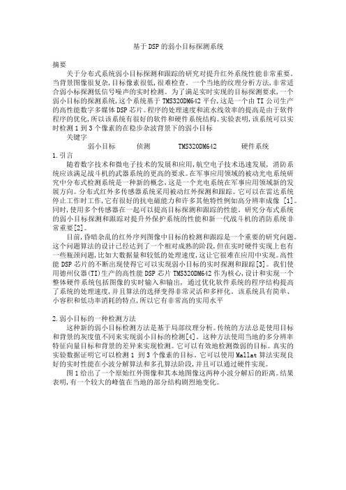
基于DSP的弱小目标探测系统摘要关于分布式系统弱小目标探测和跟踪的研究对提升红外系统性能非常重要。
当背景图像很复杂,目标像素很低,很难检查。
一个当地的纹理分析方法,非常适合弱小标探测低信号噪声的实时检测。
为了满足实时实现的目标探测要求,一个弱小目标的探测系统,这个系统基于TMS320DM642平台,这是一个由TI公司生产的高性能数字多媒体DSP芯片。
程序的处理速度和流水线效率的提高是由于软件程序的优化,所以该系统有很好的软件和硬件系统结构。
实验表明,该系统可以实时检测1到3个像素的在稳步杂波背景下的弱小目标关键字弱小目标侦测 TMS320DM642 硬件系统1.引言随着数字技术和微电子技术的发展和应用,航空电子技术迅速发展,消防系统应该满足战斗机的武器系统的更高的要求。
在军事应用领域的被动光电系统研究中分布式检测系统是一种新的概念,这是一个光电系统在军事应用领域新的发展方向。
分布式红外多传感器系统采用被动红外探测和跟踪。
它可以在雷达系统停止工作时工作,它有很好的抗电磁能力和许多其他特性例如高分辨率成像 [1]。
同时,使用多个传感器在一起可以提高目标探测和跟踪的性能。
研究分布式系统的弱小目标探测和跟踪对提升外保护系统的性能和新一代战斗机的消防系统非常重要[2]。
目前,昏暗杂乱的红外序列图像中目标的检测和跟踪是一个重要的研究问题。
这个问题算法的设计已经达到了一个相对成熟的阶段,但在实时硬件实现上也有一些瓶颈问题,比如大数据量和较低的处理速度,这让它很难在应用中实现。
高性能DSP芯片的不断出现使得它可以实现弱小目标的实时探测和跟踪[3]。
我们使用德州仪器(TI)生产的高性能DSP芯片TMS320DM642作为核心,设计和实现一个整体硬件系统包括图像的实时输入和输出, 通过优化软件系统的程序结构提高了系统的处理速度,并且算法的选择变得非常灵活和多样化。
该系统具有简单、小容积和低功率消耗的特点,所以它有非常高的实用水平2.弱小目标的一种检测方法这种新的弱小目标检测方法是基于局部纹理分析。
MEMORY存储芯片MT48LC4M32B2B5-7G中文规格书
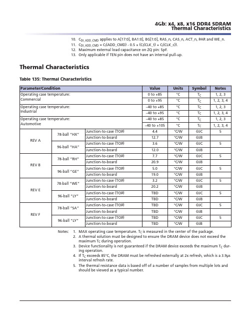
4Gb: x4, x8, x16 DDR4 SDRAM Current Specifications – Patterns and Test Conditions
A[9:7] A[6:3] A[2:0]
Toggling Static High
Data3
0
0
D 10000000000000
–
1
D 10000000000000
–
2
D_n 1 1 1 1 1 0 3 3 0 0 0 7 F 0
–
3
D_n 1 1 1 1 1 0 3 3 0 0 0 7 F 0
–
1
4–7
Notes:
1. DQS_t, DQS_c are VDDQ. 2. BG1 is a "Don't Care" for x16 devices.
3. DQ signals are VDDQ. 4. For x4 and x8 only.
13 52–55
Repeat sub-loop 0, use BG[1:0] = 3, use BA[1:0] = 2 instead4
14 56–59
Repeat sub-loop 0, use BG[1:0] = 2, use BA[1:0] = 3 instead4
15 60–63
Repeat sub-loop 0, use BG[1:0] = 3, use BA[1:0] = 0 instead4
MEMORY存储芯片MT48LC32M16A2TG-75中文规格书

Table 22: MR4 Op-Code Bit DefinitionsNotes: 1. A MODE REGISTER READ from MR4 will reset OP7 to 0.2.OP7 is reset to 0 at power-up.3.If OP2 = 1, the device temperature is greater than 85˚C.4.OP7 is set to 1 if OP[2:0] has changed at any time since the last MR4 read.5.The device might not operate properly when OP[2:0] = 000b or 111b.6.For specified operating temperature range and maximum operating temperature, referto the Operating Temperature Range table.7.LPDDR2 devices must be derated by adding 1.875ns to the following core timing param-eters: t RCD, t RC, t RAS, t RP, and t RRD. The t DQSCK parameter must be derated as speci-fied in AC Timing. Prevailing clock frequency specifications and related setup and holdtimings remain unchanged.8.The recommended frequency for reading MR4 is provided in Temperature Sensor(page 68).9.While the AT grade product is guaranteed to operate from T CASE –40°C to 105°C, thetemperature sensor accuracy relative to this is not guaranteed. The temperature sensorembedded in the LPDDR2 device is not an accurate reflection of the DRAM T CASE operat-ing temperature. Sampling of the sensor has shown up to a ±7°C variance from actualT CASE.Table 23: MR5 Basic Configuration 1 (MA[7:0] = 05h)Table 24: MR5 Op-Code Bit DefinitionsTable 11: MR0 Device Information (MA[7:0] = 00h)Table 12: MR0 Op-Code Bit DefinitionsNotes: 1.If RZQI is supported, it will be set upon completion of the MRW ZQ initialization calibra-tion.2.If ZQ is connected to V DDCA to set default calibration, OP[4:3] must be set to 01. If ZQ isnot connected to V DDCA, either OP[4:3] = 01 or OP[4:3] = 10 could indicate a ZQ-pin as-sembly error. It is recommended that the assembly error be corrected.3.In the case of a possible assembly error (either OP[4:3] = 01 or OP[4:3] = 10, as definedabove), the device will default to factory trim settings for R ON and will ignore ZQ cali-bration commands. In either case, the system might not function as intended.4.If a ZQ self test returns a value of 11b, this indicates that the device has detected a resis-tor connection to the ZQ pin. Note that this result cannot be used to validate the ZQresistor value, nor does it indicate that the ZQ resistor tolerance meets the specified lim-its (240 ohms ±1%).Table 13: MR1 Device Feature 1 (MA[7:0] = 01h)Table 14: MR1 Op-Code Bit Definitions。
MEMORY存储芯片MT48LC2M32B2TG-6A中文规格书
On-Die Termination (ODT)ODT effective resistance, R TT(EFF), is defined by bits E2 and E6 of the EMR, as shown in Figure 38 (page 83). The ODT feature is designed to improve signal integrity of thememory channel by allowing the DDR2 SDRAM controller to independently turn on/off ODT for any or all devices. R TT effective resistance values of 50˖ ˖, and 150˖ are se-lectable and apply to each DQ, DQS/DQS#, RDQS/RDQS#, UDQS/UDQS#, LDQS/LDQS#, DM, and UDM/LDM signal. Bits (E6, E2) determine what ODT resistance is en-abled by turning on/off sw1, sw2, or sw3. The ODT effective resistance value is selected by enabling switch sw1, which enables all R1 values that are 150˖ each, enabling an ef-fective resistance of 75˖ (R TT2 [EFF] = R2/2). Similarly, if sw2 is enabled, all R2 values that are 300˖ each, enable an effective ODT resistance of 150˖ (R TT2[EFF] = R2/2). Switch sw3enables R1 values of 100˖, enabling effective resistance of 50˖. Reserved states should not be used, as an unknown operation or incompatibility with future versions may re-sult.The ODT control ball is used to determine when R TT(EFF) is turned on and off, assuming ODT has been enabled via bits E2 and E6 of the EMR. The ODT feature and ODT input ball are only used during active, active power-down (both fast-exit and slow-exit modes), and precharge power-down modes of operation.ODT must be turned off prior to entering self refresh mode. During power-up and initi-alization of the DDR2 SDRAM, ODT should be disabled until the EMR command is is-sued. This will enable the ODT feature, at which point the ODT ball will determine the R TT(EFF) value. Anytime the EMR enables the ODT function, ODT may not be driven HIGH until eight clocks after the EMR has been enabled (see Figure 81 (page 130) for ODT timing diagrams).Off-Chip Driver (OCD) Impedance CalibrationThe OFF-CHIP DRIVER function is an optional DDR2 JEDEC feature not supported by Micron and thereby must be set to the default state. Enabling OCD beyond the default settings will alter the I/O drive characteristics and the timing and output I/O specifica-tions will no longer be valid (see Initialization section for proper setting of OCD de-faults).Posted CAS Additive Latency (AL)Posted CAS additive latency (AL) is supported to make the command and data bus effi-cient for sustainable bandwidths in DDR2 SDRAM. Bits E3–E5 define the value of AL, as shown in Figure 38. Bits E3–E5 allow the user to program the DDR2 SDRAM with an AL of 0, 1, 2, 3, 4, 5, or 6 clocks. Reserved states should not be used as an unknown opera-tion or incompatibility with future versions may result.In this operation, the DDR2 SDRAM allows a READ or WRITE command to be issued prior to t RCD (MIN) with the requirement that AL ื t RCD (MIN). A typical application using this feature would set AL = t RCD (MIN) - 1 × t CK. The READ or WRITE command is held for the time of the AL before it is issued internally to the DDR2 SDRAM device.RL is controlled by the sum of AL and CL; RL = AL + CL. WRITE latency (WL) is equal to RL minus one clock; WL = AL + CL - 1 × t CK. An example of RL is shown in Figure 39(page 86). An example of a WL is shown in Figure 40 (page 86).2Gb: x4, x8, x16 DDR2 SDRAM Extended Mode Register (EMR)Extended Mode Register (EMR)The extended mode register controls functions beyond those controlled by the mode register; these additional functions are DLL enable/disable, output drive strength, on-die termination (ODT), posted AL, off-chip driver impedance calibration (OCD), DQS#enable/disable, RDQS/RDQS# enable/disable, and output disable/enable. These func-tions are controlled via the bits shown in Figure 38. The EMR is programmed via the LM command and will retain the stored information until it is programmed again or the de-vice loses power. Reprogramming the EMR will not alter the contents of the memory ar-ray, provided it is performed correctly.The EMR must be loaded when all banks are idle and no bursts are in progress, and the controller must wait the specified time t MRD before initiating any subsequent opera-tion. Violating either of these requirements could result in an unspecified operation.Figure 38: EMR Definition21Notes: 1.E16 (BA2) is only applicable for densities ุ1Gb, reserved for future use, and must be pro-grammed to 0.2.Mode bits (E n ) with corresponding address balls (A n ) greater than E12 (A12) are re-served for future use and must be programmed to 0.3.Not all listed AL options are supported in any individual speed grade.4.As detailed in the Initialization section notes, during initialization of the OCD operation,all three bits must be set to 1 for the OCD default state, then set to 0 before initializa-tion is finished.2Gb: x4, x8, x16 DDR2 SDRAM Extended Mode Register (EMR)。
MEMORY存储芯片MT48LC128M4A2P-75 C中文规格书

Figure 180: WRITE (BC4) OTF to WRITE (BC4) OTF with 2t CK Preamble in Different Bank GroupCommand DQ CK_t CK_cDQS_t,DQS_cBank GroupAddress Address Notes: 1.BC4, AL = 0, CWL = 9 + 1 = 10 (see Note 7), Preamble = 2t CK.2.DI n (or b ) = data-in from column n (or column b ).3.DES commands are shown for ease of illustration; other commands may be valid atthese times.4.BC4 setting activated by MR0[1:0] = 01 and A12 = 1 during WRITE commands at T0 andT4.5.CA parity = Disable, CS to CA latency = Disable, Write DBI = Disable, Write CRC = Disable.6.The write recovery time (t WR) and write timing parameter (t WTR) are referenced fromthe first rising clock edge after the last write data shown at T18.7.When operating in 2t CK WRITE preamble mode, CWL may need to be programmed to avalue at least 1 clock greater than the lowest CWL setting supported in the applicablet CK range, which means CWL = 9 is not allowed when operating in 2t CK WRITE pream-ble mode.Figure 181: WRITE (BC4) Fixed to WRITE (BC4) Fixed with 1t CK Preamble in Different Bank GroupCommand DQ CK_t CK_cDQS_t,DQS_cBank GroupAddress Address Notes: 1.BC4, AL = 0, CWL = 9, Preamble = 1t CK.2.DI n (or b ) = data-in from column n (or column b ).5.CA parity = Disable, CS to CA latency = Disable, Write DBI = Disable, Write CRC = Disable.6.t CCD_S/L = 5 isn’t allowed in 2t CK preamble mode.7.The write recovery time (t WR) and write timing parameter (t WTR) are referenced fromthe first rising clock edge after the last write data shown at T20.8.When operating in 2t CK WRITE preamble mode, CWL may need to be programmed to avalue at least 1 clock greater than the lowest CWL setting supported in the applicablet CK range, which means CWL = 9 is not allowed when operating in 2t CK WRITE pream-ble mode.Figure 179: WRITE (BC4) OTF to WRITE (BC4) OTF with 1t CK Preamble in Different Bank GroupCommand DQ CK_t CK_cDQS_t,DQS_cBank GroupAddress Address Notes: 1.BC4, AL = 0, CWL = 9, Preamble = 1t CK.2.DI n (or b ) = data-in from column n (or column b ).3.DES commands are shown for ease of illustration; other commands may be valid atthese times.4.BC4 setting activated by MR0[1:0] = 01 and A12 = 0 during WRITE commands at T0 andT4.5.CA parity = Disable, CS to CA latency = Disable, Write DBI = Disable, Write CRC = Disable.6.The write recovery time (t WR) and write timing parameter (t WTR) are referenced fromthe first rising clock edge after the last write data shown at T17.3.DES commands are shown for ease of illustration; other commands may be valid atthese times.4.BC4 (fixed) setting activated by MR0[1:0] = 10.5.CA parity = Disable, CS to CA latency = Disable, Write DBI = Disable, Write CRC = Disable.6.The write recovery time (t WR) and write timing parameter (t WTR) are referenced fromthe first rising clock edge after the last write data shown at T15.Figure 182: WRITE (BL8) to WRITE (BC4) OTF with 1t CK Preamble in Different Bank GroupCommand DQ CK_t CK_cDQS_t,DQS_cBank GroupAddress Address Notes: 1.BL = 8/BC = 4, AL = 0, CL = 9, Preamble = 1t CK.2.DI n (or b ) = data-in from column n (or column b ).3.DES commands are shown for ease of illustration; other commands may be valid atthese times.4.BL8 setting activated by MR0[1:0] = 01 and A12 = 1 during WRITE command at T0.BC4 setting activated by MR0[1:0] = 01 and A12 = 0 during WRITE command at T4.5.CA parity = Disable, CS to CA latency = Disable, Read DBI = Disable, Write CRC = Disable.6.The write recovery time (t WR) and write timing parameter (t WTR) are referenced fromthe first rising clock edge after the last write data shown at T17.8Gb: x4, x8, x16 DDR4 SDRAM WRITE Operation。
MEMORY存储芯片MT48LC2M32B2TG-7中文规格书
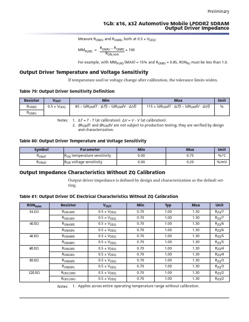
Table 81: Output Driver DC Electrical Characteristics Without ZQ Calibration
RONnom Ω Ω Ω Ω Ω Ω
Resistor RON34PD RON34PU RON40PD RON40PU RON48PD RON48PU RON60PD RON60PU RON80PD RON80PU RON120PD RON120PU
Clock Specification
The specified clock jitter is a random jitter with Gaussian distribution. Input clocks violating minimum or maximum values may result in device malfunction.
The absolute clock period, as measured from one rising clock edge to the next consecutive rising clock edge.
The average HIGH pulse width, as calculated across any 200 consecutive HIGH pulses.
Unit RZQ/7 RZQ/7 RZQ/6 RZQ/6 RZQ/5 RZQ/5 RZQ/4 RZQ/4 RZQ/3 RZQ/3 RZQ/2 RZQ/2
Preliminary
1Gb: x16, x32 Automotive Mobile LPDDR2 SDRAM Clock Specification
tJIT(cc) = max of
tCKi + 1 – tCKi
- 1、下载文档前请自行甄别文档内容的完整性,平台不提供额外的编辑、内容补充、找答案等附加服务。
- 2、"仅部分预览"的文档,不可在线预览部分如存在完整性等问题,可反馈申请退款(可完整预览的文档不适用该条件!)。
- 3、如文档侵犯您的权益,请联系客服反馈,我们会尽快为您处理(人工客服工作时间:9:00-18:30)。
SDR SDRAM
128Mb: x32 SDRAM
Features 型号:MT48LC4M32B2 – 1 Meg x 32 x 4 Banks
特征:
1.pc100-兼容;
2.完全同步;所有信号都记录在系统时钟的上升沿;
3.内部流水线操作;每一个时钟周期,可以改变列地址;
4.内部块能够隐藏行访问/预充电;
5.可编程突发长度:1,2,4,8,或整页;
6.可自动预充电,包括并发自动预充电;和自动刷新模式;
7.自刷新模式(不适用于AT器件);
8.自动刷新
—64ms, 4096-cycle refresh(商业和工业)
—16ms, 4096-cycle refresh(汽车)
9.LVTTL-兼容输入和输出;
10.单个3.3V±0.3V电源供电;
11.支持CAS1,2,和3延时(CL)。
选项标号1. 配置
--4 Meg x 32 (1 Meg x 32 x 4 banks);4M32B2 2. 封装-OCPL
--86-pin TSOP II (400 mil) TG
--86-pin TSOP II (400 mil) Pb-free P
--90-ball VFBGA (8mm x 13mm) F5
--90-ball VFBGA (8mm x 13mm) Pb-free B5
3.定时(周期)
–6ns (166 MHz) -6 A的平方–6ns (166 MHz) -6的3次方- 7ns (143 MHz) -7的3次方
4.装订:G/:L
5.工作稳定范围:
-商业(0°C to +70°C) None
-工业(–40°C to +85°C) IT
-汽车(–40°C to +105°C) AT4
注意:1. 偏离中心的分型线。
2. 仅适用于L版。
3. 仅适用于G版。
4.可用性接触微米。
表1:关键时序参数
CL = CAS延迟(读)
表2:地址表
表3:128MB(X32)SDR产品型号。