用与非门组成的3线-8线译码器课程设计
范文4.3常用组合逻辑电路(3线—8线译码器138)

• 编码: 将输入的每个高/低电平信号变成一个对应的二 进制代码
最新.
1
选通输入端 S'
I '7
I '6
I '5
状态信号 I '4
输入端
I '3
〔低电平有效〕 I '2
I '1
I '0
YS'
YE' X
最新.
74HC148
Y ' S 选通输出端
Y '2 代码输出端 Y '1 Y '0 〔低电平有效〕 Y'EX 扩展端
最新.
16
例1:利用74HC138设计一个多输出的组合逻辑电 路,输出逻辑函数式为:
Z1 AC ' A'BC AB'C Z2 BC A'B'C Z3 A'B AB'C Z4 A'BC ' B'C ' ABC
最新.
17
解:先将要输出的逻辑函数化成最小项之和的形式, 即
Z1ACABCABCm3m4m5m6 Z2 BCABCm1m3m7 Z3 ABABCm2m3m5 Z4 ABCBCABC m0m2m4m7
S2'S3'0时
Yi'(S1mi)'
最新.
12
• 利用附加控制端进展扩展 • 例:用74HC138〔3线—8线译码器〕 • 构成 4线—16线译码器
最新.
13
D3=0
Zi' mi'
最新.
D3=1
14
二、二-十进制译码器 二-十进制译码器的逻辑功能是将输入的BCD代 码译成10个高、低电平输出信号。
74LS138译码器
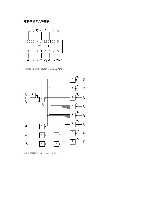
逻辑原理图及功能表:用与非门组成的3线-8线译码器74LS1383线-8线译码器74LS138的功能表无论从逻辑图还是功能表我们都可以看到74LS138的八个输出引脚,任何时刻要么全为高电平1—芯片处于不工作状态,要么只有一个为低电平0,其余7个输出引脚全为高电平1。
如果出现两个输出引脚同时为0的情况,说明该芯片已经损坏。
当附加控制门的输出为高电平(S=1)时,可由逻辑图写出由上式可以看出,同时又是这三个变量的全部最小项的译码输出,所以也把这种译码器叫做最小项译码器。
71LS138有三个附加的控制端、和。
当、时,输出为高电平(S=1),译码器处于工作状态。
否则,译码器被禁止,所有的输出端被封锁在高电平,如表3.3.5所示。
这三个控制端也叫做“片选”输入端,利用片选的作用可以将多篇连接起来以扩展译码器的功能。
带控制输入端的译码器又是一个完整的数据分配器。
在图3.3.8电路中如果把作为“数据”输入端(同时),而将作为“地址”输入端,那么从送来的数据只能通过所指定的一根输出线送出去。
这就不难理解为什么把叫做地址输入了。
例如当=101时,门的输入端除了接至输出端的一个以外全是高电平,因此的数据以反码的形式从输出,而不会被送到其他任何一个输出端上。
【例3.3.2】试用两片3线-8线译码器74LS138组成4线-16线译码器,将输入的4位二进制代码译成16个独立的低电平信号。
解:由图3.3.8可见,74LS138仅有3个地址输入端。
如果想对4位二进制代码,只能利用一个附加控制端(当中的一个)作为第四个地址输入端。
取第(1)片74LS138的和作为它的第四个地址输入端(同时令),取第(2)片的作为它的第四个地址输入端(同时令),取两片的、、,并将第(1)片的和接至,将第(2)片的接至,如图3.3.9所示,于是得到两片74LS138的输出分别为图3.3.9 用两片74LS138接成的4线-16线译码器式(3.3.8)表明时第(1)片74LS138工作而第(2)片74LS138禁止,将的0000~0111这8个代码译成8个低电平信号。
数电课程设计血型遗传规律分析电路报告

课程设计数字电子技术血型遗传分析电路年 月曰课程名称:设计题目: 院 系: 指导教师: 专 业: 学 号: 姓 名:目录第一章设计目的 .................... 第二章设计要求 .................... 第三章总体方案 .................... 第四章仿真分析 .................... 第五章具体实现 .................... 第六章心得体会 ....................参考文献第一章设计目的1.本实验设计的研究目的主要是帮助学生掌握组合逻辑电路的分析和计算方法,培养学习专业知识能力。
2.通过血型遗传规律分析电路的设计,使学生在查阅资料、设计方案、参数选择、电路制作、系统调试等方面得到训练,并使学生在电路设计方面具有进一步发挥的余地。
3.根据遗传学中血型遗传规律,设计一种血型遗传规律分析电路。
使用时,只要按钮输入一组父母的血型,仪器能立即显示出子女可能的血型第二章设计要求1、根据电路设计指标的要求,本次设计血型遗传规律分析电路考虑由常用的TTL集成电路设计,由译码电路、按钮控制输入电路、译码显示电路等组成,用探针作为显示指示灯,显示子女的可能的血型。
图1血型遗传规律分析电路设计方框图方案:血型遗传规律分析电路由两片74LS138译码器,若干与非门完成;2、方案要经济实惠,还要更加直观方便的实现电路的功能,元件尽量少, 连线布置更简单,维修方便。
第三章总体方案本设计用两片74LS138 3.8线译码器以及逻辑门设计了一种血型遗 传分析电路,电路中用单刀双掷开关控制输入端的高低电平来表示父母 的血型情况,用灯泡的亮灭代表子女的可能的血型。
实现了输入父母 血型就可以实现子女可能血型的设计。
通过用 multisim 的逻辑电路的仿 真成功完成了电路测试。
血型遗传规律分析电路总原理图如图所示:图2血型遗传电路原理图VCC5Vo o —Key = SpaceVCCVCCU3S74LSOOOX4 LED11Key = SpaceJ3-Key = S ;|>aceJ4U174LS138MI74LS13aiJ12U4C74L51DO U3C74LSOODX6咤LED其主要功能为实现血型遗传规律的电路设计,电路主要由单刀双掷开关、3,8线译码器、与非门、探针组成.其工作原理如下:AB代表父亲血型,CD代表母亲血型,则一共有16种血型配对的可能,所以本实验采用两片74LS138(译码器)级联,可完成4输入16输出功能在电路设计上,我们从子女的血型可能性入手,设计输出六组信号,每一组代表在父母的血型影响下孩子可能出现的血型根据设计指标中提供的血型配对表格, 可多得到以下结果:实验电路图中对应的ProdeXI代表——B型和0型。
仿真用与非门组成的3-8译码器(74HC138)

贵州大学
电路EDA电路技术课程考
核报告
姓名:田泽民
学号:PZ082014131 班级:08级计维班
一、实验目的:
1、会PSpice软件的仿真应用。
2、知道全加器的原理,进行仿
真。
二、实验名称:
仿真用与非门组成的3-8译码器(74HC138)。
三、实验内容:
画出电路图,进行参数的设置,截图,分析得到仿真结果。
四、实验原理:
译码器74HC138有三个附加的控制端,当状态为(1,0,0)时,译码器工作。
输入端A2,A1,A0;输出端Y0,Y1,Y2,Y3,Y4,Y5,Y6,Y7.
五、实验过程:
1、实验电路:
2、参数设置:
DSTM4、DSTM5、DSTM6高低电平交互的时间分别设为:4ms、2ms 和1ms,0—30ms,步长为5ms
3、仿真结果:
从上图可以看出,当输入端为000的时候选择Y0输出,当输入端为001的时候选择Y1输出……
010 Y2 011 Y3 100 Y4
101 Y5 110 Y6 111 Y7
4、真值表对照:
5、结果截图(与理论值相符):
六、实验结论:
本次实验,所得到的显示结果与预计:完全相同,因而证明本次实验是正确的。
七、实验总结:
进行参数设置的时候,时间不能设得太短,最好是以(ms)为单位。
在输入端时间设置应该注意取到每个输入组合,否则实验就不一定仿真出真实的结果。
3 8译码器
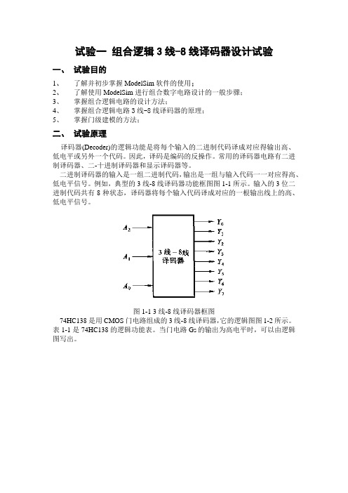
试验一组合逻辑3线-8线译码器设计试验一、试验目的1、了解并初步掌握ModelSim软件的使用;2、了解使用ModelSim进行组合数字电路设计的一般步骤;3、掌握组合逻辑电路的设计方法;4、掌握组合逻辑电路3线-8线译码器的原理;5、掌握门级建模的方法;二、试验原理译码器(Decoder)的逻辑功能是将每个输入的二进制代码译成对应得输出高、低电平或另外一个代码。
因此,译码是编码的反操作。
常用的译码器电路有二进制译码器、二-十进制译码器和显示译码器等。
二进制译码器的输入是一组二进制代码,输出是一组与输入代码一一对应得高、低电平信号。
例如,典型的3线-8线译码器功能框图图1-1所示。
输入的3位二进制代码共有8种状态,译码器将每个输入代码译成对应的一根输出线上的高、低电平信号。
图1-1 3线-8线译码器框图74HC138是用CMOS门电路组成的3线-8线译码器,它的逻辑图图1-2所示。
表1-1是74HC138的逻辑功能表。
当门电路G S的输出为高电平时,可以由逻辑图写出。
图1-2 74HC138逻辑功能图表1-1 74HC138逻辑功能表由上式可以看出,由''07Y Y -同时又是210,,A A A 这三个变量的全部最小项的译码输出,所以也将这种译码器称为最小项译码器。
74HC138有3个附加的控制端''123,S S S 和。
当''123S 1,S S 0=+=时,s G 输出为高电平,译码器处于工作状态。
否则,译码器被禁止,所有的输出端被封锁为高电平。
这3个控制端也称为“片选”输入端,利用片选的作用可以将多片连接起来以扩展译码器的功能;三、 预习要求1、数字电子技术基础组合逻辑电路设计一般设计方法;2、74HC138的逻辑功能;3、门级建模的一般方法和基本语句;4、ModelSim 软件的一般使用方法(ModelSim SE Tutorial);四、 实验步骤(一)、熟悉ModelSim 软件环境 1、建立一个新Project1-1双击左面快捷方式或者电击[程序]/[ModelSim SE 6.1f]/[ModelSim]启动ModelSim 6.1(如图1-3);注意:必须首先关闭IMPORTANT Information 对话框才能开始其它操作;图1-31-2 [File]/[New]/[Project…]新建一个project,会弹出Create Project对话框(如图1-4);图1-4⏹Project Name(项目名称)需要填入你所建立的项目的名称;⏹指定项目所在路径;如果所指定的目录不存在,会弹出对话框提示是否建立这个目录;一般选择是;⏹缺省的工作库名;注意:1、路径一般不应包含汉字;2、逻辑应在ModelSim的安装目录下指定;3、缺省的工作库的名称一般不需要改动;2、载入HDL元文件2-1设定好1-2步骤的每项内容后,点击OK,弹出Add items to the Projects对话框;如图1-5所示。
0级《数字逻辑电路》实验指导书 1
课程名称:数字逻辑电路实验指导书课时:8学时集成电路芯片一、简介数字电路实验中所用到的集成芯片都是双列直插式的,其引脚排列规则如图1-1所示。
识别方法是:正对集成电路型号(如74LS20)或看标记(左边的缺口或小圆点标记),从左下角开始按逆时针方向以1,2,3,…依次排列到最后一般排在左上端,接地一脚(在左上角)。
在标准形TTL集成电路中,电源端VCC,7脚为GND。
若集端GND一般排在右下端。
如74LS20为14脚芯片,14脚为VCC成芯片引脚上的功能标号为NC,则表示该引脚为空脚,与内部电路不连接。
二、TTL集成电路使用规则1、接插集成块时,要认清定位标记,不得插反。
2、电源电压使用范围为+4.5V~+5.5V之间,实验中要求使用Vcc=+5V。
电源极性绝对不允许接错。
3、闲置输入端处理方法(1)悬空,相当于正逻辑“1”,对于一般小规模集成电路的数据输入端,实验时允许悬空处理。
但易受外界干扰,导致电路的逻辑功能不正常。
因此,对于接有长线的输入端,中规模以上的集成电路和使用集成电路较多的复杂电路,所有控制输入端必须按逻辑要求接入电路,不允许悬空。
(也可以串入一只1~10KΩ的固定电阻)或接至某一固定(2)直接接电源电压VCC电压(+2.4≤V≤4.5V)的电源上,或与输入端为接地的多余与非门的输出端相接。
(3)若前级驱动能力允许,可以与使用的输入端并联。
4、输入端通过电阻接地,电阻值的大小将直接影响电路所处的状态。
当R ≤680Ω时,输入端相当于逻辑“0”;当R≥4.7KΩ时,输入端相当于逻辑“1”。
对于不同系列的器件,要求的阻值不同。
5、输出端不允许并联使用(集电极开路门(OC)和三态输出门电路(3S)除外)。
否则不仅会使电路逻辑功能混乱,并会导致器件损坏。
6、输出端不允许直接接地或直接接+5V电源,否则将损坏器件,有时为了使后,一般取R=3~5.1K 级电路获得较高的输出电平,允许输出端通过电阻R接至VccΩ。
译码器设计组合逻辑电路案例分析
译码器设计组合逻辑电路案例分析【信息单】一、编码器在数字系统中,把二进制码按一定的规律编排,使每组代码具有特定的含义,称为编码。
具有编码功能的逻辑电路称为编码器。
编码器是一个多输入多输出的组合逻辑电路。
按照编码方式不同,编码器可分为普通编码器和优先编码器;按照输出代码种类的不同,可分为二进制编码器和非二进制编码器。
1.普通编码器普通编码器分二进制编码器和非二进制编码器。
若输入信号的个数N 与输出变量的位数n 满足N =2n ,此电路称为二进制编码器;若输入信号的个数N 与输出变量的位数n 不满足N =2n ,此电路称为非二进制编码器。
普通编码器任何时刻只能对其中一个输入信息进行编码,即输入的N 个信号是互相排斥的。
若编码器输入为4个信号,输出为两位代码,则称为4线-2线编码器(或4/2线编码器)。
2.优先编码器优先编码器是当多个输入端同时有信号时,电路只对其中优先级别最高的信号进行编码的编码器。
3.集成编码器10线-4线集成优先编码器常见型号为54/74147、54/74LS147,8线-3线常见型号为54/74148、54/74LS148。
4.编码器举例(1)键控8421BCD 码编码器10个按键S 0~S 9代表输入的10个十进制数0~9,输入为低电平有效,即某一按键按下,对应的输入信号为0,输出对应的8421码,输出为4位码,所以有4个输出端A 、B 、C 、D 。
真值表见表7.1,由真值表写出各输出的逻辑表达式为 9898S S S S =+=A76547654S S S S S S S S =+++=B 76327632S S S S S S S S =+++=C 9753197531S S S S S S S S S S =++++=D表7.1键控8421BCD 码编码器真值表(2)二进制编码器用n 位二进制代码对2n 个信号进行编码的电路称为二进制编码器。
3位二进制编码器有 8个输入端3个输出端,所以常称为8线—3线编码器,其功能真值表见表7.2,输入为高电平有效。
三八译码器的结构、原理与设计_毕业论文

题目:三八译码器的结构、原理与设计学院:物理学院专业:电子科学与技术姓名:董少雨指导教师:赵宏亮完成日期:2014年5月20日毕业论文任务书毕业论文题目:三八译码器的结构、原理与设计选题意义、创新性、科学性和可行性论证:如今全球信息化的步伐正在不断加快,数字信号的产生、变换等方面应用的更加广泛。
三八译码器在信号处理方面起着十分重要的作用。
本文主要阐述三八译码器的基本结构和工作原理,并通过对时序逻辑电路设计方法的研究,完成三八译码器的设计。
主要内容:译码器的种类与特点,三八译码器的结构和工作原理,最后完成了三八译码器的设计。
目的要求:1、熟悉三八译码器的发展背景和趋势。
2、掌握各类译码器的工作性能。
3、了解三八译码器的基本结构和工作原理。
4、学会时序逻辑电路的设计方法。
计划进度:2013年12月21日~2014年2月25日,确定毕业论文选题,并搜集资料,查阅相关文献;2014年2月26日~4月10日,写出论文总体大纲,运用软件得到仿真数据;2014年4月11日~4月25日,论文撰写;提交初稿;2014年4月26日~5月19日,修改论文,论文定稿,准备答辩。
指导教师签字:主管院长(系主任)签字:2013年12 月25 日辽宁大学本科毕业论文(设计)指导记录表论文题目三八译码器的结构、原理与设计学生姓名董少雨学号101002103 年级、专业10级电子科学与技术指导教师姓名赵宏亮指导教师职称讲师所在院系物理学院第一次指导(对确定题目、毕业论文(设计)任务书的指导意见):由于以前对三八译码器有所了解,《三八译码器的结构、原理与设计》题目符合毕业论文设计的要求。
研究三八译码器可以加强对数字集成电路的了解,毕业论文进度安排合理,接下来按照进度写出论文总体大纲。
指导方式:(请选择)面谈√电话电子邮件指导教师签字:2013年12月24日第二次指导(对论文提纲的指导意见):查阅相关资料,进一步地掌握三八译码器的基本结构和工作原理,三八译码器的设计方法十分合理,要熟悉掌握相关软件的使用并从中得到相关数据。
用译码器设计组合逻辑电路例题
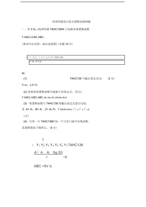
用译码器设计组合逻辑电路例题一、用3线—8线译码器74HC138W门电路实现逻辑函数Y A/B/C/ A/ BC/ ABC。
(要求写出过程,画出连接图)(本题10分)解:(1) 74HC138勺输出表达式为:(2分) Y i/ m:(i 0~7)(2) 将要求的逻辑函数写成最小项表达式:(2分)Y A/B/C/ A/BC/ ABC m0 m2 m7 (m0m1/m7)/(3) 将逻辑函数与74HC138的输出表达式进行比较:设A= A2、B= A1、C= A0,得:Y (m0m1/m7)/ (丫0/丫2/丫7/)/(2分)(4) 可用一片74HC138H加一个与非门就可实现函数。
其逻辑图如下图所示。
(4分)t丫。
Y1 Y2 Y3 Y4 Y5 Y a Y7 74HC138A〉A〔A。
Sg S3r ~0ABC +5V d.三、公司A 、8 C 三个股东,分别占有50% 30咧日20%勺股份,试用一片3线-8 线译码器74HC138^若干门电路设计一个三输入三输出的多数表决器, 用丁开会 时按股份大小记分输出通过、平■局和否决三种表决结果。
通过、平■局和否决,分 别用X 、Y 、Z 表示(股东赞成和输出结果均用1表示)。
(12分)(3)画连线图(4分)令 74HC138的地址码 A 2 A,A 1 B,A 0 CX AB /C ABC / ABC 74HC138 A- A* S 〔 Sg S3 == | 二 午 ABC +5Vm 5 m 6 m 7 (m 5m ;m 7),Y A /BC AB /C / ABC m 3 mu/ / / \ / (m 3m 4) Z A /B /C / A /B /C A /BC / m 0 m 1 m 2 (m 0m ;m ;)/解:(2)歹0写表达式(4四、某学校学生参加三门课程A、B、C的考试,根据课程学时不同,三门课程考试及格分别可得2、4、5分,不及格均为0分,若总得分大丁等丁7分,便可结业。
仿真用与非门组成的3-8译码器(74HC138)
贵州大学
电路EDA电路技术课程考
核报告
姓名:田泽民
学号:PZ082014131 班级:08级计维班
一、实验目的:
1、会PSpice软件的仿真应用。
2、知道全加器的原理,进行仿
真。
二、实验名称:
仿真用与非门组成的3-8译码器(74HC138)。
三、实验内容:
画出电路图,进行参数的设置,截图,分析得到仿真结果。
四、实验原理:
译码器74HC138有三个附加的控制端,当状态为(1,0,0)时,译码器工作。
输入端A2,A1,A0;输出端Y0,Y1,Y2,Y3,Y4,Y5,Y6,Y7.
五、实验过程:
1、实验电路:
2、参数设置:
DSTM4、DSTM5、DSTM6高低电平交互的时间分别设为:4ms、2ms 和1ms,0—30ms,步长为5ms
3、仿真结果:
从上图可以看出,当输入端为000的时候选择Y0输出,当输入端为001的时候选择Y1输出……
010 Y2 011 Y3 100 Y4
101 Y5 110 Y6 111 Y7
4、真值表对照:
5、结果截图(与理论值相符):
六、实验结论:
本次实验,所得到的显示结果与预计:完全相同,因而证明本次实验是正确的。
七、实验总结:
进行参数设置的时候,时间不能设得太短,最好是以(ms)为单位。
在输入端时间设置应该注意取到每个输入组合,否则实验就不一定仿真出真实的结果。
[数字电子技术及应用(第2版)习题答案第2单元习题答案
自我检测题一、填空题2-1如果对键盘上108个符号进行二进制编码,则至少要 7 位二进制数码。
2-2共阳LED 数码管应由输出 低 电平的七段显示译码器来驱动点亮,而共阴LED 数码管应采用输出为 高 电平的七段显示译码器来驱动点亮。
2-3采用54LS138完成数据分配器的功能时,若把S 1作为数据输入端接D ,则应将使能端2S 接 低 电平,3S 接 低 电平。
2-4对N 个信号进行编码时,需要使用的二进制代码位数n 要满足条件 N ≤2n 。
二、选择题2-5一个8选1的数据选择器,其地址输入端有几个 B 。
A 、1 B 、3 C 、2 D 、42-6可以用 B 、C 电路的芯片来实现一个三变量组合逻辑函数。
A 、编码器 B 、译码器 C 、数据选择器2-7要实现一个三变量组合逻辑函数,可选用 A 芯片。
A 、74LS138 B 、54LS148 C 、74LS147 三、判断题2-8 54/74LS138是输出低电平有效的3线-8线译码器。
( ✓ )2-9当共阳极LED 数码管的七段(a ~g )阴极电平依次为1001111时,数码管将显示数字1。
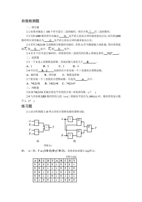
(✓ )练习题2-1试分析图题2-10所示各组合逻辑电路的逻辑功能。
图题2-1解:(a )图,)()(D C B A Y ⊕⊕⊕=,真值表如表题2-1(a)所示:表题2-1(a)A B C DYABY(a )(b )(a )图为四变量奇校验器,当输入变量中有奇数个为1,输出为1。
(b )图,AB B A B A B A Y +=+++=,真值表如表题2-1(b)所示:(b )图为同或门电路,当输入变量状态相同时出1,相反时出0。
2-2试分析图题2-2所示各组合逻辑电路的逻辑功能,写出函数表达式。
图题2-2解:(a)图0=+++=CD C B AB Y(b)图C B A Y C B A AB C B A AB Y ⊕⊕=⊕+=⊕∙=21,)()(2-3试采用与非门设计下列逻辑电路:(1)三变量非一致电路;(2)三变量判奇电路(含1的个数); (3)三变量多数表决电路。
级《数字逻辑电路》实验指导书
课程名称:数字逻辑电路实验指导书课时:8学时集成电路芯片一、简介数字电路实验中所用到的集成芯片都是双列直插式的,其引脚排列规则如图1-1所示。
识别方法是:正对集成电路型号<如74LS20)或看标记<左边的缺口或小圆点标记),从左下角开始按逆时针方向以1,2,3,…依次排列到最后一脚<在左上角)。
在标准形TTL集成电路中,电源端V一般排在左上CC,7脚为端,接地端GND一般排在右下端。
如74LS20为14脚芯片,14脚为VCCGND。
若集成芯片引脚上的功能标号为NC,则表示该引脚为空脚,与内部电路不连接。
二、TTL集成电路使用规则1、接插集成块时,要认清定位标记,不得插反。
2、电源电压使用范围为+4.5V~+5.5V之间,实验中要求使用Vcc=+5V。
电源极性绝对不允许接错。
3、闲置输入端处理方法(1> 悬空,相当于正逻辑“1”,对于一般小规模集成电路的数据输入端,实验时允许悬空处理。
但易受外界干扰,导致电路的逻辑功能不正常。
因此,对于接有长线的输入端,中规模以上的集成电路和使用集成电路较多的复杂电路,所有控制输入端必须按逻辑要求接入电路,不允许悬空。
<也可以串入一只1~10KΩ的固定电阻)或接至某一 (2> 直接接电源电压VCC固定电压(+2.4≤V≤4.5V>的电源上,或与输入端为接地的多余与非门的输出端相接。
(3> 若前级驱动能力允许,可以与使用的输入端并联。
4、输入端通过电阻接地,电阻值的大小将直接影响电路所处的状态。
当R ≤680Ω时,输入端相当于逻辑“0”;当R≥4.7 KΩ时,输入端相当于逻辑“1”。
对于不同系列的器件,要求的阻值不同。
5、输出端不允许并联使用<集电极开路门(OC>和三态输出门电路(3S>除外)。
否则不仅会使电路逻辑功能混乱,并会导致器件损坏。
6、输出端不允许直接接地或直接接+5V电源,否则将损坏器件,有时为,一般取R 了使后级电路获得较高的输出电平,允许输出端通过电阻R接至Vcc=3~5.1 KΩ。
3-8译码器的设计实验报告
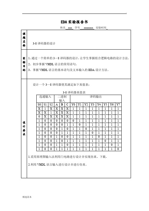
EDA实验报告书姓名 xxx 学号 xxxxxxx 实验时间课题名称3-8译码器的设计实验目的1、通过一个简单的3-8译码器的设计,让学生掌握组合逻辑电路的设计方法。
2、初步掌握VHDL语言的常用语句。
3、掌握VHDL语言的基本语句及文本输入的EDA设计方法。
设计要求设计一个3—8译码器使其满足如下真值表:3-8译码器真值表选通输入二进制输入译码输出S0 S1 S2 A B C Y0 Y1 Y2 Y3 Y4 Y5 Y6 Y7X 1 X X X X 1 1 1 1 1 1 1 1X X 1 X X X 1 1 1 1 1 1 1 10 X X X X X 1 1 1 1 1 1 1 11 0 0 0 0 0 0 1 1 1 1 1 1 11 0 0 0 0 1 1 0 1 1 1 1 1 11 0 0 0 1 0 1 1 0 1 1 1 1 11 0 0 0 1 1 1 1 1 0 1 1 1 11 0 0 1 0 0 1 1 1 1 0 1 1 11 0 0 1 0 1 1 1 1 1 1 0 1 11 0 0 1 1 0 1 1 1 1 1 1 0 11 0 0 1 1 1 1 1 1 1 1 1 1 01.采用原理图输入法利用门电路进行设计并实现仿真、下载。
2.利用VHDL语言输入进行设计并进行仿真。
设计思路1、根据74138的功能,当S0=1,S1=0,S2=0时译码器处于工作状态。
否则译码器被禁止,所有输出端被封锁在高电平。
由真值表画出卡诺图,再写出对应表达式,再画出电路。
2、使用VHDL语言时,应注意头文件以及各种输入的格式,使用IF语句,CASE语句设计电路,最后再用END语句结束程序。
设计原理图及源程序LIBRARY IEEE;USE IEEE.STD_LOGIC_1164.ALL;USE IEEE.STD_LOGIC_UNSIGNED.ALL;ENTITY SA ISPORT(D:IN STD_LOGIC_VECTOR(2 DOWNTO 0);S0,S1,S2:IN STD_LOGIC;Y:OUT STD_LOGIC_VECTOR(7 DOWNTO 0));END ;ARCHITECTURE XIANI OF SA ISBEGINPROCESS(D,S0,S1,S2)BEGINIF (S0='0')THEN Y<="11111111";ELSIF(S0='1' AND S1='0' AND S2='0')THENIF (D(2)='0' AND D(1)='0' AND D(0)='0')THEN Y<="01111111";ELSIF (D(2)='0' AND D(1)='0' AND D(0)='1')THEN Y<="10111111";ELSIF (D(2)='0' AND D(1)='1' AND D(0)='0')THEN Y<="11011111";ELSIF (D(2)='0' AND D(1)='1' AND D(0)='1')THEN Y<="11101111";ELSIF (D(2)='1' AND D(1)='0' AND D(0)='0')THEN Y<="11110111";ELSIF (D(2)='1' AND D(1)='0' AND D(0)='1')THEN Y<="11111011";ELSIF (D(2)='1' AND D(1)='1' AND D(0)='0')THEN Y<="11111101";ELSIF (D(2)='1' AND D(1)='1' AND D(0)='1')THEN Y<="11111110";ELSE Y<="ZZZZZZZZ";END IF;ELSE Y<="ZZZZZZZZ";END IF;END PROCESS;END;仿真波形图实验结果问题讨论比较此实验中两种输入法哪种要好一些,好在哪里?答:使用与非门设计电路对应延时比使用程序对应延时时间短,原因是程序的每步执行都需要一定的时间,其时间比调用库中的与非门所需时间长。
3~8线译码器和非门实现逻辑函数
3~8线译码器和非门实现逻辑函数3~8线译码器是非门电路的实际应用之一,它可以将输入信号转换为数字信号。
下面是一个简单的逻辑函数实现,使用3~8线译码器和非门:假设我们有一个输入信号X,该信号由3个比特(二进制位)表示。
我们需要将该信号转换为一个二进制数,以便我们可以进行后续的逻辑运算。
首先,我们将非门和非门连接在一起,以将输入信号X转换为输出信号Y。
具体而言,我们将非门的输出设置为0,输入设置为1,此时Y的输出将等于X的异或。
接下来,我们需要将Y的每个比特转换为一个二进制数,以便我们可以进行逻辑运算。
我们可以使用一个三输入三输出的计数器来实现这一点。
计数器的每个输入连接到非门的输入端,每个输出连接到Y的每个比特的输入端。
具体而言,计数器的第1个输入连接到非门的第1个输入端口,第2个输入连接到非门的第2个输入端口,第3个输入连接到非门的第3个输入端口。
计数器的每个输出连接到Y的对应比特的输入端口。
当计数器达到0时,Y的每个比特都将被转换为0,因为非门的输出设置为0,输入设置为1。
我们可以使用一个组合逻辑框架来实现这一点,将每个计数器的输出连接到一组逻辑门,以实现逻辑运算。
具体而言,我们可以使用一个4位计数器,其中每个计数器的输出连接到一个与非门,以实现0、1、0、1的组合逻辑运算。
例如,如果我们需要将Y的比特转换为0、1、0、1中的一个,我们可以使用如下配置:```Y T10 T9 T8 T7------ ------ ------ ------0 | | | |1 | | | |0 | | | |1 | | | |0 | | | |1 | | | |T1 ------ T2 ------ T3 ------ T40 | X | 0 | 0 |1 | X | 1 | 1 |0 | 0 | X | 0 |1 | 1 | 0 | X |0 | 1 | 1 | 1 |1 | 0 | 1 | 0 |```在这个例子中,X的比特数为3,因此我们需要将X转换为0、1、0、1中的一个。
译码器及其应用实验报告
实验二译码器及其使用一.实验目的1.掌握译码器的测试方法。
2.了解中规模集成译码器的管脚分布,掌握其逻辑功能。
3.掌握译码器构成组合电路的方法。
4.学习译码器的扩展。
二.实验设备及器件。
1.数字逻辑电路实验板1块。
2.74HC(LS)20(四二输入与非门)一片。
3.74HC(LS)138(3-8译码器)二片。
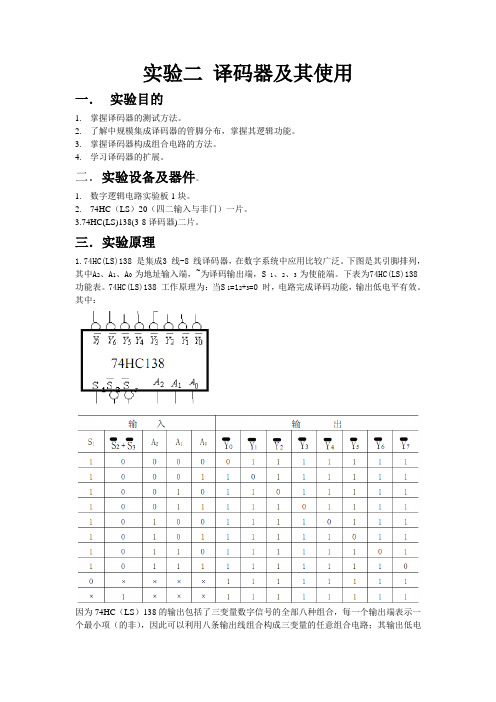
三.实验原理1.74HC(LS)138 是集成3 线-8 线译码器,在数字系统中应用比较广泛。
下图是其引脚排列,其中A2、A1、A0 为地址输入端,~为译码输出端,S 1、2、3 为使能端。
下表为74HC(LS)138 功能表。
74HC(LS)138 工作原理为:当S 1=12+3=0 时,电路完成译码功能,输出低电平有效。
其中:因为74HC(LS)138的输出包括了三变量数字信号的全部八种组合,每一个输出端表示一个最小项(的非),因此可以利用八条输出线组合构成三变量的任意组合电路;其输出低电平有效。
2.实验用器件管脚介绍:74HC(LS)20(二四输入与非门)管脚如下图所示。
四.实验内容1.逻辑功能测试将输出端接到发光二极管上,然后从000~111依次输入译码器,然后改变输出线与8个端口的链接,探索发光规律。
如:当输入为010时(A2=0,A1=1,A0=0),输出线接在Y2(非)时发光,即其输出为低电平。
2. 用74HC(LS)138实现逻辑函数(基本命题)Y=AB+BC+CA由k 图知:Y=m3+m5+m6+m7=Y3*Y5*Y6*Y7————所以在译码器上有ABC=A2A1A0,而在译码器的输出端,将Y3,Y5,Y6,Y7————接到四二与非门的输入端,四二与非门的输出端接入发光二极管即可完成逻辑电路。
由于LED 是低电平有效,所以选中时Y 输出高电平,LED 反而不发光,未选中时LED 灯发光。
3、扩展(扩展命题)用两个3 线-8 线译码器构成4 线-16 线译码器根据该图连接逻辑电路,然后对电路进行测试其是否达到预期效果。
课程设计报告---四人表决器的设计

课程设计报告---四人表决器的设计四人表决器的设计设计要求某特殊足球评委会由一位教练和三位球迷组成,对裁判员的判罚进行表决时,当满足以下条件即表示同意:(1)有三人或三人以上同意;(2)有两人同意,但其中一人必须是教练。
1、方案论证与对比1(1 方案一1.1.1 设计电路如图21.2 方案二用2输入与非门设计,同样可根据表2的真值表作卡诺图以及它的逻辑函数表达式,这里省略没作,因为与方案一比劣势明显。
该方案的电路图如下:图1 2输入与非门接线图11.3 方案对比与选择该电路的原理和方案一的区别不大,只是这个全部用的2输入与非门来实现,这个方案中其一元器件使用太过单一,而方案一中用了译码器74HC138,这就使我们更加的熟悉了译码器的适用。
其二方案一也大大减少了连线的交叉程度,方案二中因为一个芯片中含有几个与非门,只用一个又太浪费,全部用连线就会有很多交叉,使得用protel布线时带来很大的困难。
所以综合以上两个原因我们选择了方案一。
2、分析与设计2、1 译码器结构分析四人表决器即要求四个输入端,三个球迷用三线-八线的译码器,但教练的[1] 身份比较特别,为使电路简单就直接接逻辑开关。
74HC138是3线-8线译码器,其功能表如表1所示。
该译码器有3位二进制输入A0,A1,A2,它们共有8种状态的组合,即可译出8个输出信号Y0-Y7,输出为低电平有效。
此外,还设计了E3、E2和E13个是能输入端,为电路功能的扩展提供了方便。
由功能表可知,当E3=1,且E2=E1=0时,译码器处于工作状[2]态。
由功能表可得:Y0=E3*E2*E1*A2*A1*A0根据各输出的逻辑表达式可以写出最初的逻辑表达式,根据学校元件库能提供的元件,对逻辑表达式化简,于是最终确定完成本次设计的所有元器件,然后画出原理图,见图1该表清楚的表达出74HC138的逻辑功能,即三输入八输出和使能端的有效电平,同时说明了74HC138的工作状态和输出有效电平。
[数字电子技术及应用(第2版)习题答案第2单元习题答案

[数字电子技术及应用(第2版)习题答案第2单元习题答案自我检测题一、填空题2-1如果对键盘上108个符号进行二进制编码,则至少要 7 位二进制数码。
2-2共阳LED 数码管应由输出 低 电平的七段显示译码器来驱动点亮,而共阴LED 数码管应采用输出为 高 电平的七段显示译码器来驱动点亮。
2-3采用54LS138完成数据分配器的功能时,若把S 1作为数据输入端接D ,则应将使能端2S 接 低 电平,3S 接 低 电平。
2-4对N 个信号进行编码时,需要使用的二进制代码位数n 要满足条件 N ≤2n 。
二、选择题2-5一个8选1的数据选择器,其地址输入端有几个 B 。
A 、1B 、3C 、2D 、42-6可以用 B 、C 电路的芯片来实现一个三变量组合逻辑函数。
A 、编码器B 、译码器C 、数据选择器2-7要实现一个三变量组合逻辑函数,可选用 A 芯片。
A 、74LS138B 、54LS148C 、74LS147 三、判断题2-8 54/74LS138是输出低电平有效的3线-8线译码器。
( ✓ )2-9当共阳极LED 数码管的七段(a ~g )阴极电平依次为1001111时,数码管将显示数字1。
(✓ ) 练习题2-1试分析图题2-10所示各组合逻辑电路的逻辑功能。
A B C DYABY图题2-1解:(a)图,)⊕=,真值表如表题2-1(a)A⊕Y⊕B)((DC所示:表题2-1(a)(a)图为四变量奇校验器,当输入变量中有奇数个为1,输出为1。
(b)图CB A YC B A AB C B A AB Y ⊕⊕=⊕+=⊕•=21,)()(2-3试采用与非门设计下列逻辑电路: (1)三变量非一致电路;(2)三变量判奇电路(含1的个数); (3)三变量多数表决电路。
解:(1)设A 、B 、C 为输入变量,当输入不一致时输出为1,一致时为0,真值表如表题2-3(1)所示:表题2-3(1) A B C Y 0 0 0 0 0 0 1 1 0 1 0 1 0 1 1 1 1 0 0 1 1 0 1 1 1 1 0 1 111函数式为:ABC C B A ABC C B A Y •=+= 电路图如图题2-3(1)所示:(2)设A、B、C为输入变量,当输入奇数个1时输出为,否则为0,真值表如表题2-3(2)所示:表题2-3(2)A B C Y0 0 0 00 0 1 10 1 0 10 1 1 01 0 0 11 0 1 01 1 0 01 1 1 1函数式为:ABCBABCAY••+++=•=ABCCBABCACBACABC电路图如图题2-3(2)所示:(3)设A、B、C为输入变量(设“1”表示同意,“0”表示不同意),Y为输出变量(设“1”表示通过,“0”表示不通过),真值表如表题2-3(3)所示:表题2-3(3)A B C Y0 0 0 00 0 1 00 1 0 00 1 1 11 0 0 01 0 1 11 1 0 11 1 1 1函数式为:BC•=A+Y•=+++=+BCACBCABAABACBABCCABC电路图如图题2-3(3)所示:2-4有一个车间,有红、黄两个故障指示灯,用来表示三台设备的工作情况。
用与非门组成的3线-8线译码器课程设计
⽤与⾮门组成的3线-8线译码器课程设计哈尔滨理⼯⼤学软件学院课程设计报告课程数字IC设计(双语)题⽬ 3线-8线译码器班级集成12—1专业集成电路设计与集成系统学⽣张铭学号 1214020130 指导教师陆学斌2014年12⽉31⽇⽬录1、课程设计⽬的介绍………………………………………………2、课程设计题⽬介绍………………………………………………3、课程设计报告内容………………………………………………4、体会总结…………………………………………………………5、参考书⽬…………………………………………………………1.课程设计⽬的训练学⽣综合运⽤学过的数字集成电路的基本知识,独⽴设计相对复杂的数字集成电路的能⼒。
2.课程设计题⽬⽤与⾮门组成的3线-8线译码器3.课程设计报告内容3.1 设计要求按题⽬要求的逻辑功能进⾏设计,电路各个组成部分须有设计说明;必须采⽤⽹表输⼊法;3.2 设计内容拿到题⽬后⾸先进⾏电路设计。
然后在微机上进⾏HSPICE⽹表输⼊、编译和软件仿真,满⾜设计要求。
3.3 查找有关书籍设计电路原理图3.4 根据原理图编写⽹表*74 HC138.include 'd:\lib\180nm_bulk.l'.param Supply=1.8.global Vdd Gnd.opt scale=0.1uVdd Vdd Gnd 'Supply'.subckt nand ina inb inc ind outmpa out ina Vdd Vdd PMOS l=2 w=8 ad=8 pd=8 as=40 ps=40 mpb out inb Vdd Vdd PMOS l=2 w=8 ad=8 pd=8 as=40 ps=40 mpc out inc Vdd Vdd PMOS l=2 w=8 ad=8 pd=8 as=40 ps=40 mpd out ind Vdd Vdd PMOS l=2 w=8 ad=8 pd=8 as=40 ps=40 mna out ina x Gnd NMOS l=2 w=16 ad=16 pd=16 as=80 ps=80 mnb x inb y Gnd NMOS l=2 w=16 ad=16 pd=16 as=80 ps=80 mnc y inc z Gnd NMOS l=2 w=16 ad=16 pd=16 as=80 ps=80 mnd z ind Gnd Gnd NMOS l=2 w=16 ad=16 pd=16 as=80 ps=80 .ends.subckt nor ina inb inc outmpa out ina x Vdd PMOS l=2 w=12 ad=12 pd=12 as=60 ps=60 mpb x inb y Vdd PMOS l=2 w=12 ad=12 pd=12 as=60 ps=60 mpc y inc Vdd Vdd PMOS l=2 w=12 ad=12 pd=12 as=60 ps=60 mna out ina Gnd Gnd NMOS l=2 w=2 ad=2 pd=2 as=10ps=10 mnb out inb Gnd Gnd NMOS l=2 w=2 ad=2 pd=2 as=10 ps=10 mnc out inc Gnd Gnd NMOS l=2 w=2 ad=2 pd=2 as=10 ps=10 .ends.subckt Inverter in outmpa out in Vdd Vdd PMOS l=2 w=4 ad=4 pd=4 as=20 ps=20 mpb out in Gnd Gnd NMOS l=2 w=2 ad=4 pd=4 as=10 ps=10.endsx1 s1 s1b Inverterx2 s1b s2b s3b s norx3 a0 a0b Inverterx4 a1 a1b Inverterx5 a2 a2b Inverterx6 a0b a0bb Inverterx7 a1b a1bb Inverterx8 a2b a2bb Inverterx9 a0b a1b a2b s y0b nandx10 a0bb a1b a2b s y1b nandx11 a0b a1bb a2b s y2b nandx12 a0bb a1bb a2b s y3b nandx13 a0b a1b a2bb s y4b nandx14 a1b a2bb a0bb s y5b nandx15 a0b a2bb a1bb s y6b nandx16 a1bb a0bb a2bb s y7b nandCinv y1b Gnd 6000fVs1 s1 Gnd pulse 0 'Supply' 7.5ns 200ps 200ps 130ns 140ns Vs2b s2b Gnd pulse 'Supply' 0 0ns 200ps 200ps 100ns 110ns Vs3b s3b Gnd pulse 'Supply' 0 0ns 200ps 200ps 65ns 75ns Va0 a0 Gnd pulse 0 'Supply' 0ns 200ps 200ps 17.5ns 35ns Va1 a1 Gnd pulse 0 'Supply' 0ns 200ps 200ps 40ns 80ns Va2 a2 Gnd pulse 0 'Supply' 0ns 200ps 200ps 70ns 140ns .tran 100ps 140ns.plot tran V(s1).end3.5画图编写3线—8线译码器的功能表说明:s1 s2b s3b 为附加的控制端,当s1 = 1,s2b + s3b = 0时,译码器处于⼯作状态,否则译码器被禁⽌,所有的输出端被封锁在⾼电平。
- 1、下载文档前请自行甄别文档内容的完整性,平台不提供额外的编辑、内容补充、找答案等附加服务。
- 2、"仅部分预览"的文档,不可在线预览部分如存在完整性等问题,可反馈申请退款(可完整预览的文档不适用该条件!)。
- 3、如文档侵犯您的权益,请联系客服反馈,我们会尽快为您处理(人工客服工作时间:9:00-18:30)。
哈尔滨理工大学
软件学院
课程设计报告
课程数字IC设计(双语)
题目 3线-8线译码器
班级集成12—1
专业集成电路设计与集成系统学生张铭
学号 1214020130 指导教师陆学斌
2014年12月31日
目录
1、课程设计目的介绍………………………………………………
2、课程设计题目介绍………………………………………………
3、课程设计报告内容………………………………………………
4、体会总结…………………………………………………………
5、参考书目…………………………………………………………
1.课程设计目的
训练学生综合运用学过的数字集成电路的基本知识,独立设计相对复杂的数字集成电路的能力。
2.课程设计题目
用与非门组成的3线-8线译码器
3.课程设计报告内容
3.1 设计要求
按题目要求的逻辑功能进行设计,电路各个组成部分须有设计说明;
必须采用网表输入法;
3.2 设计内容
拿到题目后首先进行电路设计。
然后在微机上进行HSPICE网表输入、编译和软件仿真,满足设计要求。
3.3 查找有关书籍设计电路原理图
3.4 根据原理图编写网表
*74 HC138
.include 'd:\lib\180nm_bulk.l'
.param Supply=1.8
.global Vdd Gnd
.opt scale=0.1u
Vdd Vdd Gnd 'Supply'
.subckt nand ina inb inc ind out
mpa out ina Vdd Vdd PMOS l=2 w=8 ad=8 pd=8 as=40 ps=40 mpb out inb Vdd Vdd PMOS l=2 w=8 ad=8 pd=8 as=40 ps=40 mpc out inc Vdd Vdd PMOS l=2 w=8 ad=8 pd=8 as=40 ps=40 mpd out ind Vdd Vdd PMOS l=2 w=8 ad=8 pd=8 as=40 ps=40 mna out ina x Gnd NMOS l=2 w=16 ad=16 pd=16 as=80 ps=80 mnb x inb y Gnd NMOS l=2 w=16 ad=16 pd=16 as=80 ps=80 mnc y inc z Gnd NMOS l=2 w=16 ad=16 pd=16 as=80 ps=80 mnd z ind Gnd Gnd NMOS l=2 w=16 ad=16 pd=16 as=80 ps=80 .ends
.subckt nor ina inb inc out
mpa out ina x Vdd PMOS l=2 w=12 ad=12 pd=12 as=60 ps=60 mpb x inb y Vdd PMOS l=2 w=12 ad=12 pd=12 as=60 ps=60 mpc y inc Vdd Vdd PMOS l=2 w=12 ad=12 pd=12 as=60 ps=60 mna out ina Gnd Gnd NMOS l=2 w=2 ad=2 pd=2 as=10 ps=10 mnb out inb Gnd Gnd NMOS l=2 w=2 ad=2 pd=2 as=10 ps=10 mnc out inc Gnd Gnd NMOS l=2 w=2 ad=2 pd=2 as=10 ps=10 .ends
.subckt Inverter in out
mpa out in Vdd Vdd PMOS l=2 w=4 ad=4 pd=4 as=20 ps=20 mpb out in Gnd Gnd NMOS l=2 w=2 ad=4 pd=4 as=10 ps=10 .ends
x1 s1 s1b Inverter
x2 s1b s2b s3b s nor
x3 a0 a0b Inverter
x4 a1 a1b Inverter
x5 a2 a2b Inverter
x6 a0b a0bb Inverter
x7 a1b a1bb Inverter
x8 a2b a2bb Inverter
x9 a0b a1b a2b s y0b nand
x10 a0bb a1b a2b s y1b nand
x11 a0b a1bb a2b s y2b nand
x12 a0bb a1bb a2b s y3b nand
x13 a0b a1b a2bb s y4b nand
x14 a1b a2bb a0bb s y5b nand
x15 a0b a2bb a1bb s y6b nand
x16 a1bb a0bb a2bb s y7b nand
Cinv y1b Gnd 6000f
Vs1 s1 Gnd pulse 0 'Supply' 7.5ns 200ps 200ps 130ns 140ns Vs2b s2b Gnd pulse 'Supply' 0 0ns 200ps 200ps 100ns 110ns Vs3b s3b Gnd pulse 'Supply' 0 0ns 200ps 200ps 65ns 75ns Va0 a0 Gnd pulse 0 'Supply' 0ns 200ps 200ps 17.5ns 35ns Va1 a1 Gnd pulse 0 'Supply' 0ns 200ps 200ps 40ns 80ns Va2 a2 Gnd pulse 0 'Supply' 0ns 200ps 200ps 70ns 140ns .tran 100ps 140ns
.plot tran V(s1)
.end
3.5画图编写3线—8线译码器的功能表
说明:s1 s2b s3b 为附加的控制端,当s1 = 1,s2b + s3b = 0时,译码器处于工作状态,否则译码器被禁止,所有的输出端被封锁在高电平。
这三个控制端也称为“片选”输入端,利用片选的作用可以将多片连接起来以扩展译码器的功能。
3.6用HSPICE和COSMOS-SCOPE进行仿真与功能表对比
a2 a1 a0 = 0 0 0 y0b = 0
a2 a1 a0 = 0 0 1 y1b = 0
a2 a1 a0 = 0 1 0 y2b = 0
a2 a1 a0 = 0 1 1 y3b = 0
a2 a1 a0 = 1 0 0 y4b = 0
a2 a1 a0 = 1 0 1 y5b = 0
a2 a1 a0 = 1 1 0 y6b = 0
a2 a1 a0 = 1 1 1 y7b = 0
通过仿真图与功能表的对比,可以证明译码器逻辑功能的正确性。
3.7优化通路延时
设输入端的电容为C
inv ,输出端的负载电容为5000C
inv
,从输入到输出任意找
一通路,优化通路延时,手工计算确定通路中每个门对应的晶体管的尺寸。
选择a0至y2b这一通路手动计算过程如下:
优化后与优化前的延时对比
优化后:上升延时 5.1ns 下降延时 185ps
优化前:上升延时 8.5ns 下降延时 3.1ns
4.总结
本次课程设计使我对课堂上的理论知识有了进一步的了解,并增强了对数字IC这门课程的兴趣。
但同时也暴露出我对知识点的掌握还不足等缺点。
加上在设计过程中遇到了一些问题,使得我必须查找相关资料,从而增长知识的同时也增强了解决问题和动手的能力,锻炼了做事细心、用心、耐心的能耐。
这一课程设计,使我向更高的精神和知识层次迈向一大步。
所以在以后的学习生活中,我会努力学习,培养自己独立思考的能力,积极参加多种设计活动,培养自己的综合能力,从而使得自己成为一个有综合能力的人才而更加适应社会。
最后,我要感谢各位老师的指导,谢谢!本次设计的顺利完成,离不开各位老师、同学们的帮助,在此,向老师、同学们表示感谢。
还要感谢学院、系为我们提供了一个良好的学习氛围和人文环境,这对我们以后的学习、工作、生活都会具有重要影响!
5.参考书目
[1]David A.Hodge, Analysis and Design of Digital Integrated Circuits in Deep Submicron Technology. Thrid Edition, 清华大学出版社,2006年
[2]阎石,《数字电子技术基础》,高等教育出版社,2006年。