flash外文翻译 英文文献 外文文献
单片机温度控制系统毕业论文中英文资料外文翻译文献

单片机温度控制系统中英文资料外文翻译文献英文原文DescriptionThe at89s52 is a low-power, high-performance CMOS 8-bit microcomputer with 4K bytes of Flash Programmable and Erasable Read Only Memory (PEROM) and 128 bytes RAM. The device is manufactured using Atmel’s h igh density nonvolatile memory technology and is compatible with the industry standard MCS-51™ instruction set and pinout. The chip combines a versatile 8-bit CPU with Flash on a monolithic chip, the Atmelat89s52 is a powerful microcomputer which provides a highly flexible and cost effective solution to many embedded control applications.Features:• Compatible with MCS-51™ Products• 4K Bytes of In-System Reprogrammable Flash Memory• Endurance: 1,000 Write/Erase Cycles• Fully Static Operation: 0 Hz to 24 MHz• Three-Level Program Memory Lock• 128 x 8-Bit Internal RAM• 32 Programmable I/O Lines• Two 16-Bit Timer/Counters• Six Interrupt Sources• Programmable Serial Channel• Low Power Idle and Power Down ModesThe at89s52 provides the following standard features: 4K bytes of Flash, 128 bytes of RAM, 32 I/O lines, two 16-bit timer/counters, a five vectortwo-level interrupt architecture, a full duplex serial port, on-chip oscillator and clock circuitry. In addition, the at89s52 is designed with static logic for operation down to zero frequency and supports two software selectable power saving modes. The Idle Mode stops the CPU while allowing the RAM, timer/counters, serial port and interrupt system to continue functioning. The Power Down Mode saves the RAM contents but freezes the oscillator disabling all other chip functions until the next hardware reset.Pin Description:VCC Supply voltage.GND Ground.Port 0Port 0 is an 8-bit open drain bidirectional I/O port. As an output port each pin can sink eight TTL inputs. When is are written to port 0 pins, the pins can be used as high impedance inputs.Port 0 may also be configured to be the multiplexed loworderaddress/data bus during accesses to external program and data memory. In this mode P0 has internal pullups.Port 0 also receives the code bytes during Flash programming, and outputs the code bytes during program verification. External pullups are required during program verification.Port 1Port 1 is an 8-bit bidirectional I/O port with internal pullups. The Port 1 output buffers can sink/source four TTL inputs. When 1s are written to Port 1 pins they are pulled high by the internal pullups and can be used as inputs. As inputs, Port 1 pins that are externally being pulled low will source current (IIL) because of the internal pullups.Port 1 also receives the low-order address bytes during Flash programming and verification.Port 2Port 2 is an 8-bit bidirectional I/O port with internal pullups. The Port 2 output buffers can sink/source four TTL inputs. When 1s are written to Port 2 pins they are pulled high by the internal pullups and can be used as inputs. As inputs, Port 2 pins that are externally being pulled low will source current (IIL) because of the internal pullups.Port 2 emits the high-order address byte during fetches from external program memory and during accesses to external data memory that use 16-bit addresses (MOVX @ DPTR). In this application it uses strong internalpull-ups when emitting 1s. During accesses to external data memory that use 8-bit addresses (MOVX @ RI), Port 2 emits the contents of the P2 Special Function Register.Port 2 also receives the high-order address bits and some control signals during Flash programming and verification.Port 3Port 3 is an 8-bit bidirectional I/O port with internal pullups. The Port 3 output buffers can sink/source four TTL inputs. When 1s are written to Port 3 pins they are pulled high by the internal pullups and can be used as inputs. As inputs, Port 3 pins that are externally being pulled low will source current (IIL) because of the pullups.Port 3 also serves the functions of various special features of theat89s52 as listed below:Port 3 also receives some control signals for Flash programming andverification.RSTReset input. A high on this pin for two machine cycles while theoscillator is running resets the device.ALE/PROGAddress Latch Enable output pulse for latching the low byte of theaddress during accesses to external memory. This pin is also the program pulse input (PROG) during Flash programming.In normal operation ALE is emitted at a constant rate of 1/6 theoscillator frequency, and may be used for external timing or clockingpurposes. Note, however, that one ALE pulse is skipped during each access to external Data Memory.If desired, ALE operation can be disabled by setting bit 0 of SFRlocation 8EH. With the bit set, ALE is active only during a MOVX or MOVC instruction. Otherwise, the pin is weakly pulled high. Setting the ALE-disable bit has no effect if the microcontroller is in external execution mode.PSENProgram Store Enable is the read strobe to external program memory. When the at89s52 is executing code from external program memory, PSEN is activated twice each machine cycle, except that two PSENactivations are skipped during each access to external data memory.EA/VPPExternal Access Enable. EA must be strapped to GND in order to enable the device to fetch code from external program memory locations starting at 0000H up to FFFFH. Note, however, that if lock bit 1 is programmed, EA will be internally latched on reset. Port pinalternate functions P3.0rxd (serial input port) P3.1txd (serial output port) P3.2^int0 (external interrupt0) P3.3^int1 (external interrupt1) P3.4t0 (timer0 external input) P3.5t1 (timer1 external input) P3.6^WR (external data memory write strobe) P3.7 ^rd (external data memory read strobe)EA should be strapped to VCC for internal program executions.This pin also receives the 12-volt programming enable voltage(VPP) during Flash programming, for parts that require 12-volt VPP.XTAL1Input to the inverting oscillator amplifier and input to the internal clock operating circuit.XTAL2Output from the inverting oscillator amplifier.Oscillator CharacteristicsXTAL1 and XTAL2 are the input and output, respectively, of an inverting amplifier which can be configured for use as an on-chip oscillator, as shown in Figure 1. Either a quartz crystal or ceramic resonator may be used. To drive the device from an external clock source, XTAL2 should be left unconnected while XTAL1 is driven as shown in Figure 2. There are no requirements on the duty cycle of the external clock signal, since the input to the internal clocking circuitry is through a divide-by-two flip-flop, but minimum and maximum voltage high and low time specifications must be observed.Idle ModeIn idle mode, the CPU puts itself to sleep while all the onchip peripherals remain active. The mode is invoked by software. The content of the on-chip RAM and all the special functions registers remain unchanged during this mode. The idle mode can be terminated by any enabled interrupt or by a hardware reset.It should be noted that when idle is terminated by a hard ware reset, the device normally resumes program execution, from where it left off, up to two machine cycles before the internal reset algorithm takes control. On-chip hardware inhibits access to internal RAM in this event, but access to the port pins is not inhibited. To eliminate the possibility of an unexpected write to a port pin when Idle is terminated by reset, the instruction following the one that invokes Idle should not be one that writes to a port pin or to external memory.Status of External Pins During Idle and Power Down Modesmode Program memory ALE ^psen Port0 Port1Port2Port3idle internal 1 1 data data data Data Idle External 1 1 float Data data Data Power down Internal 0 0 Data Data Data Data Power down External 0 0 float data Data data Power Down ModeIn the power down mode the oscillator is stopped, and the instructionthat invokes power down is the last instruction executed. The on-chip RAMand Special Function Registers retain their values until the power down modeis terminated. The only exit from power down is a hardware reset. Resetredefines the SFRs but does not change the on-chip RAM. The reset shouldnot be activated before VCC is restored to its normal operating level andmust be held active long enough to allow the oscillator to restart andstabilize.Program Memory Lock BitsOn the chip are three lock bits which can be left unprogrammed (U) orcan be programmed (P) to obtain the additional features listed in the tablebelow:Lock Bit Protection ModesWhen lock bit 1 is programmed, the logic level at the EA pin issampled and latched during reset. If the device is powered up without a reset,the latch initializes to a random value, and holds that value until reset isactivated. It is necessary that the latched value of EA be in agreement with the current logic level at that pin in order for the device to function properly. Programming the Flash:The at89s52 is normally shipped with the on-chip Flash memory array in the erased state (that is, contents = FFH) and ready to be programmed.The programming interface accepts either a high-voltage (12-volt) or alow-voltage (VCC) program enable signal.The low voltage programming mode provides a convenient way to program the at89s52 inside the user’s system, while the high-voltage programming mode is compatible with conventional third party Flash or EPROM programmers.The at89s52 is shipped with either the high-voltage or low-voltage programming mode enabled. The respective top-side marking and device signature codes are listed in the following table.Vpp=12v Vpp=5vTop-side mark at89s52xxxxyywwat89s52xxxx-5yywwsignature (030H)=1EH(031H)=51H(032H)=FFH (030H)=1EH (031H)=51H (032H)=05HThe at89s52 code memory array is programmed byte-bybyte in either programming mode. To program any nonblank byte in the on-chip Flash Programmable and Erasable Read Only Memory, the entire memory must be erased using the Chip Erase Mode.Programming Algorithm:Before programming the at89s52, the address, data and control signals should be set up according to the Flash programming mode table and Figures 3 and 4. To program the at89s52, take the following steps.1. Input the desired memory location on the address lines.2. Input the appropriate data byte on the data lines.3. Activate the correct combination of control signals.4. Raise EA/VPP to 12V for the high-voltage programming mode.5. Pulse ALE/PROG once to program a byte in the Flash array or the lock bits. The byte-write cycle is self-timed and typically takes no more than 1.5 ms. Repeat steps 1 through 5, changing the address and data for the entire array or until the end of the object file is reached.Data Polling: The at89s52 features Data Polling to indicate the end of a write cycle. During a write cycle, an attempted read of the last byte written will result in the complement of the written datum on PO.7. Once the write cycle has been completed, true data are valid on all outputs, and the next cycle may begin. Data Polling may begin any time after a write cycle has been initiated.Ready/Busy: The progress of byte programming can also be monitored by the RDY/BSY output signal. P3.4 is pulled low after ALE goes high during programming to indicate BUSY. P3.4 is pulled high again when programming is done to indicate READY.Program Verify: If lock bits LB1 and LB2 have not been programmed, the programmed code data can be read back via the address and data lines for verification. The lock bits cannot be verified directly. Verification of the lock bits is achieved by observing that their features are enabled.Chip Erase: T he entire Flash Programmable and Erasable Read Only Memory array is erased electrically by using the proper combination of control signals and by holding ALE/PROG low for 10 ms. The code array is written with all “1”s. The chip erase operation must be executed before the code memory can be re-programmed.Reading the Signature Bytes: The signature bytes are read by the same procedure as a normal verification of locations 030H, 031H, and 032H, except that P3.6 and P3.7 must be pulled to a logic low. The values returned are as follows.(030H) = 1EH indicates manufactured by Atmel(031H) = 51H indicates 89C51(032H) = FFH indicates 12V programming(032H) = 05H indicates 5V programmingProgramming InterfaceEvery code byte in the Flash array can be written and the entire array can be erased by using the appropriate combination of control signals. The write operation cycle is selftimed and once initiated, will automatically time itself to completion.中文翻译描述at89s52是美国ATMEL公司生产的低电压,高性能CMOS8位单片机,片内含4Kbytes的快速可擦写的只读程序存储器(PEROM)和128 bytes 的随机存取数据存储器(RAM),器件采用ATMEL公司的高密度、非易失性存储技术生产,兼容标准MCS-51产品指令系统,片内置通用8位中央处理器(CPU)和flish存储单元,功能强大at89s52单片机可为您提供许多高性价比的应用场合,可灵活应用于各种控制领域。
自动化专业单片机相关外文文献英文文献外文翻译中英对照

使用本科生毕业论文V外文翻译)译文名称:MCS -51系列单片机地功能和结构专业:自动化班次:学员:指导教员:评阅人:完成时间:2018年11月30日Structure and function of the MCS-51 seriesStructure and function of the MCS-51 series one-chip computer is a name of a piece of on e-chip computer series which In tel Compa ny produces. This compa ny in troduced 8 top-grade on e-chip computers of MCS-51 series in 1980 after introducing 8 one-chip computers of MCS-48 series in 1976. It belong to a lot of kinds this line of on e-chip computer the chips have,such as 8051,8031, 8751, 80C51BH, 80C31BH,etc., their basic composition, basic performance and in structi on system are all the same. 8051 daily represe ntatives-51 serial on e-chip computers b5E2RGbCAPAn one-chip computer system is made up of several following parts: ( 1> One microprocessor of 8 (CPU>. ( 2> At slice data memory RAM (128B/256B>,it use not depositting not can reading /data that write, such as result not middle of operati on, final result and data wan ted to show, etc. ( 3> Procedure memory ROM/EPROM (4KB/8KB >, is used to preserve the procedure , some initial data and form in slice. But does not take ROM/EPROM within some on e-chip computers, such as 8031 , 8032, 80C ,etc.. (4> Four 8 run side by side I/O in terface P0 four P3, each mouth can use as introduction , may use as exporting too. ( 5> Two timer / counter, each timer / coun ter may set up and count in the way, used to count to the exter nal in cide nt, can set up into a timing way too, and can according to count or result of timing realize the control of the computer. ( 6> Five cut off cutting off the control system of the source . ( 7> One all duplexing serial I/O mouth of UART (uni versal asynchronous receiver/tra nsmitter (UART> >, is it realize on e-chip computer or on e-chip computer and serial com muni catio n of computer to use for. ( 8> Stretch oscillator and clock produce circuit, quartz crystal finely tune electric capacity n eed outer. Allow oscillati on freque ncy as 12 megahertas now at most. Every the above-me nti oned part was joined through the in side data bus .Among them, CPU is a core of the one-chip computer, it is the control of the computer and comma nd cen tre, made up of such parts as arithmeticunit and使用controller , etc.. The arithmetic unit can carry on 8 persons of arithmetic operation and unit ALU of logic operation while including one, the 1 storing device temporarilies of 8, stori ng device 2 temporarily, 8's accumulatio n device ACC, register B and procedure stateregister PSW, etc. Pers on who accumulate ACC count by 2 in put ends en tered of check ing etc. temporarily as one operation often, come from person who store 1 operation is it is it make operation to go on to count temporarily , operation result and loopback ACC withanother one. In addition, ACC is often regarded as the transfer station of data tran smissi on on 8051 in side . The same as gen eral microprocessor, it is the busiest register. Help rememberi ng that agree ing with A expresses in the order. The con troller in cludes the procedure coun ter , the order is depositted, the order decipher, the oscillator and timing circuit, etc. The procedure counter is made up of coun ter of 8 for two, amounts to 16. Itis a byte address coun ter of the procedure in fact, the content is the next IA that will carried out in PC. The content which cha nges it can cha nge the directi on that the procedure carries out . Shake the circuit in 8051 one-chip computers, only need outer quartz crystal and freque ncy to fin ely tune the electric capacity, its freque ncy range is its12MHZ of 1.2MHZ. This pulse signal, as 8051 basic beats of working, namely the minimum unit of time. 8051 is the same as other computers, the work in harmony under the control of the basic beat, just like an orchestra accord ing to the beat play that is comma nded&nqFDPw There are ROM (procedure memory , can only read > and RAM in 8051 slices (data memory, can is it can write > two to read, they have each in depe ndent memory address space, dispose way to be the same with gen eral memory of computer. Procedure 8051 memory and 8751 slice procedure memory capacity 4KB, address begin from 0000H, used for preserving the procedure and form con sta nt. Data 8051- 8751 8031 of memory data memory 128B, address false 00FH, use for middle result to deposit operation, the data are stored temporarily and the data are buffered etc.. In RAM of this 128B,使用there is unit of 32 byteses that can be appo in ted as the job register, this and gen eral microprocessor is differe nt, 8051 slice RAM and job register rank one formation the same to arrange the location. It is not very the same that the memory of MCS-51 series one-chip computer and general computer disposes the way in additi on. Gen eral computer for first address space, ROM and RAM can arrange in differe nt space with in the range of this address at will, n amely the addresses of ROM and RAM, with distributing different address space ina formation. While visiting the memory, corresponding and only an address Memory unit, canROM, it can be RAM too, and by visiting the order similarly. This kind of memory structure is called the structure of Princeton. 8051 memories are divided into procedure memory space and data memory space on the physics structure, there are four memory spaces in all: The procedure stores in one and data memory space outside data memory and one in procedure memory space and one outside one, the structure forms of this kind of procedure device and data memory separated form data memory, called Harvard structure. But use the an gle from users, 8051 memory address space is divided into three kin ds: (1> In the slice, arrange blocks of FFFFH , 0000H of locati on , in unison outside the slice (use 16 addresses>. (2> The data memory address space outside one of 64KB, the address is arran ged from 0000H 64KB FFFFH (with 16 addresses> too to the location. (3> Data memory address space of 256B (use 8 addresses>. Three above-mentioned memory space addresses overlap, for distinguishing and designing the order symbol of different data transmission in the instruction system of 8051: CPU visit slice, ROM order spend MOVC , visit block RAM order uses MOVX outside the slice, RAM order uses MOV to visit in slice. DXDiTa9E3d8051 one-chip computer have four 8 walk abreast I/O port, call P0, P1, P2 and P3. Each port is 8 accurate two-way mouths, accounts for 32 pins altogether. Every one I/O line can be used as introduction and exported in depe nden tly. Each port in cludes a latch (n amely special fun cti on register >,使用one exports the driver and a introduction buffer . Make data can latch when outputting, data can buffer when making introduction , but four function of passway these self-same. Expa nd among the system of memory outside hav ing slice, four port these may serve as accurate two-way mouth of I/O in com mon use. Expand among the system of memory outside having slice, P2 mouth see high 8 address off= P0 mouth is a two-way bus, send the in troduct ion of 8 low addresses and data / export in timesharingr crpuDGiTThe circuit of 8051 on e-chip computers and four I/O ports is very ingenious in design. Familiar with I/O port logical circuit, not only help to use ports correctly and rati on ally, and will in spire to desig ning the peripheral logical circuit of on e-chip computer to some exte nt. Load ability and in terface of port have certa in requireme nt, because output grade, P0 of mouth and P1 end output, P3 of mouth grade differe nt at structure, so,the load ability and in terface of its door dema nd to have nothing in com mon with each other. P0 mouth is differe nt from other mouths, its output grade draws the resistance supremly. When using it as the mouth in com mon use to use, output grade is it leak circuit to turn on, is it is it urge NMOS draw the resistance on taking to be outer with it while in putt ing to go out to fail. When being used as in troductio n, should write "1" to a latch first. Every one with P0 mouth can drive 8 Model LS TTL load to export. P1 mouth is an accurate two-way mouth too, used as I/O in com mon use. Different from P0 mouth output of circuit its, draw load resistance link with power on in side have. In fact, the resista nce is that two effects are in charge of FET and together: One FET is in charge of load, its resistance is regular. Another one can is it lead to work with close at two state, make its Preside nt resista nce value cha nge approximate 0 or group value heavy two situation very. When it is 0 that the resistance is approximate , can draw the pin to the high level fast。
电气工程及其自动化专业 外文文献 英文文献 外文翻译 plc方面
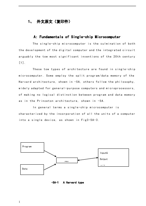
1、外文原文(复印件)A: Fundamentals of Single-chip MicrocomputerTh e si ng le-ch i p mi cr oc om pu ter is t he c ul mi nat i on o f bo th t h e d ev el op me nt o f th e d ig it al com p ut er an d t he int e gr at ed ci rc ui ta r gu ab ly th e t ow m os t s i gn if ic ant i nv en ti on s o f t h e 20t h c en tu ry[1].Th es e to w typ e s of a rc hi te ctu r e ar e fo un d i n s in gl e-ch ip m i cr oc om pu te r. So m e em pl oy t he sp l it p ro gr am/d ata me mo ry o f th e H a rv ar d ar ch it ect u re, sh ow n i n -5A, ot he rs fo ll ow th e ph i lo so ph y, w i de ly a da pt ed fo r g en er al-p ur pos e c om pu te rs an d m i cr op ro ce ss or s, o f m a ki ng no lo gi c al di st in ct io n b e tw ee n p ro gr am a n d da t a m em ory a s i n th e Pr in cet o n ar ch it ec tu re,sh ow n in-5A.In g en er al te r ms a s in gl e-chi p m ic ro co mp ut er i sc h ar ac te ri zed b y the i nc or po ra tio n of al l t he uni t s o f a co mp ut er i n to a s in gl e dev i ce, as s ho wn in Fi g3-5A-3.-5A-1 A Harvard type-5A. A conventional Princeton computerFig3-5A-3. Principal features of a microcomputerRead only memory (ROM).R OM i s u su al ly f or th e p er ma ne nt, n o n-vo la ti le s tor a ge o f an a pp lic a ti on s pr og ra m .M an ym i cr oc om pu te rs an d mi cr oc on tr ol le r s a re in t en de d fo r h ig h-v ol ume a p pl ic at io ns a nd h en ce t he e co nom i ca l ma nu fa ct ure of t he d ev ic es r e qu ir es t ha t the co nt en ts o f the pr og ra m me mo ry b e co mm it te dp e rm an en tl y d ur in g th e m an uf ac tu re o f c hi ps . Cl ear l y, th is im pl ie sa ri g or ou s a pp roa c h t o R OM co de d e ve lo pm en t s in ce c ha ng es ca nn otb e m ad e af te r man u fa ct ur e .T hi s d e ve lo pm en t pr oce s s ma y in vo lv e e m ul at io n us in g a s op hi st ic at ed deve lo pm en t sy st em w i th a ha rd wa re e m ul at io n ca pa bil i ty a s we ll a s th e u se of po we rf ul so ft wa re t oo ls.So me m an uf act u re rs p ro vi de ad d it io na l RO M opt i on s byi n cl ud in g i n th ei r ra ng e de vi ce s wi th (or i nt en de d fo r us e wi th) u s er pr og ra mm ab le m em or y. Th e s im p le st of th es e i s us ua ll y d ev ice w h ic h ca n op er ate in a m ic ro pr oce s so r mo de b y usi n g so me o f th e i n pu t/ou tp ut li ne s as a n ad dr es s an d da ta b us f or acc e ss in g e xt er na l m e mo ry. T hi s t ype o f d ev ic e c an b e ha ve fu nc ti on al l y a s t he si ng le c h ip mi cr oc om pu te r fr om wh ic h i t i s de ri ve d a lb eit w it h r es tr ic ted I/O an d a mo di fie d e xt er na l ci rcu i t. T he u se o f t h es e RO Ml es sd e vi ce s is c om mo n e ve n in p ro du ct io n c ir cu it s wh er e t he v ol um e do es n o t ju st if y th e d e ve lo pm en t co sts of c us to m on-ch i p RO M[2];t he re c a n st il l b e a si g ni fi ca nt s a vi ng in I/O a nd ot he r c hi ps co mp ar ed t o a c on ve nt io nal mi cr op ro ce ss or b as ed c ir cu it. M o re e xa ctr e pl ac em en t fo r RO M d ev ic es c an b e o bt ai ne d in t he f o rm o f va ri an ts w i th 'pi gg y-ba ck'EP RO M(Er as ab le p ro gr am ma bl e ROM)s oc ke ts o rd e vi ce s w it h EP ROM i ns te ad o f R OM 。
动画专业外语文献

动画专业外语文献关于动画专业的外语文献有很多,以下是一些例子:1. "The Art of Animation: The Evolution of the American Feature Film" by John Lasseter (Disney Editions, 2001)2. "The Art of Storyboard: The Complete Guide for Filmmakers and Storyboard Artists" by David B. Levy (Focal Press, 2014)3. "The Animator's Survival Kit: A Manual for Drawing and Thinking" by Richard Williams (Faber and Faber, 2001)4. "The Encyclopedia of Animated Cartoons" by John Cawelti (Facts on File, 1993)5. "The World Encyclopedia of Cartoons" by Gary Groth and Michael Vollmer (Facts on File, 1993)6. "The Animator's Handbook: A Complete Guide to Creating and Developing the Art of Animation" by Don L. Harris (Focal Press, 2003)7. "The Art of SpongeBob SquarePants: The Complete Collection" by The SpongeBob SquarePants Writers' Room (Chronicle Books, 2007)8. "The Art of the Simpsons: The Complete History of the Iconic Characters, Writers, Animators, and Producers Behind the Longest-Running Animated Series" by John Ortved (Hachettespeakersbureau, 2015)9. "The Animator's Eye: A Handbook for Visual Development" by John Lasseter (Focal Press, 1985)10. "The Illusion of Life: Disney Animation" by Ollie Johnston and Frank Thomas (Disney Editions, 1981)这些书籍涵盖了动画的历史、技术和理论等方面,对于深入了解动画专业非常有帮助。
fpga英文文献翻译
Field-programmable gate array(现场可编程门阵列)1、History ——历史FPGA业界的可编程只读存储器(PROM)和可编程逻辑器件(PLD)萌芽。
可编程只读存储器(PROM)和可编程逻辑器件(PLD)都可以分批在工厂或在现场(现场可编程)编程,然而,可编程逻辑被硬线连接在逻辑门之间。
在80年代末期,为海军水面作战部提供经费的的史蒂夫·卡斯尔曼提出要开发将实现60万可再编程门计算机实验。
卡斯尔曼是成功的,并且与系统有关的专利是在1992年发行的。
1985年,大卫·W·佩奇和卢文R.彼得森获得专利,一些行业的基本概念和可编程逻辑阵列,门,逻辑块技术公司开始成立。
同年,Xilinx共同创始人,Ross Freeman和Bernard Vonderschmitt发明了第一个商业上可行的现场可编程门阵列——XC2064。
该XC2064可实现可编程门与其它门之间可编程互连,是一个新的技术和市场的开端。
XC2064有一个64位可配置逻辑块(CLB),有两个三输入查找表(LUT)。
20多年后,Ross Freeman 进入全国发明家名人堂,名人堂对他的发明赞誉不绝。
Xilinx继续受到挑战,并从1985年到90年代中期迅速增长,当竞争对手如雨后春笋般成立,削弱了显著的市场份额。
到1993年,Actel大约占市场的18%。
上世纪90年代是FPGA的爆炸性时期,无论是在复杂性和生产量。
在90年代初期,FPGA的电信和网络进行了初步应用。
到这个十年结束时,FPGA行业领袖们以他们的方式进入消费电子,汽车和工业应用。
1997年,一个在苏塞克斯大学工作的研究员阿德里安·汤普森,合并遗传算法技术和FPGA来创建一个声音识别装置,使得FPGA的名气可见一斑。
汤姆逊的算法配置10×10的细胞在Xilinx的FPGA芯片阵列,以两个音区分,利用数字芯片的模拟功能。
单片机交通灯中英文对照外文翻译文献
中英文对照外文翻译原文DESIGN OF TRAFFIC LIGHT BASED ON MCUBecause of the rapid development of our economy resulting in the car number of large and medium-sized cities surged and the urban traffic, is facing serious test, leading to the traffic problem increasingly serious, its basically are behaved as follows: traffic accident frequency, to the human life safety enormous threat, Traffic congestion, resulting in serious travel time increases, energy consumption increase; Air pollution and noise pollution degree of deepening, etc. Daily traffic jams become people commonplace and had to endure. In this context, in combination with the actual situation of urban road traffic, develop truly suitable for our own characteristics of intelligent signal control system has become the main task.PrefaceIn practical application at home and abroad, according to the actual traffic signal control application inspection, planar independent intersection signal control basic using set cycle, much time set cycle, half induction, whole sensor etc in several ways. The former two control mode is completely based on planar intersection always traffic flow data of statistical investigation, due to traffic flow the existence of variable sex and randomicity, the two methods have traffic efficiency is low, the scheme, the defects of aging and half inductive and all the inductive the two methods are in the former two ways based on increased vehicle detector and according to the information provided to adjust cycle is long and green letter of vehicle, it than random arrived adaptability bigger, can make vehicles in the parking cord before as few parking, achieve traffic flowing effectIn modern industrial production,current,voltage,temperature, pressure, and flow rate, velocity, and switch quantity are common mainly controlled parameter. For example: in metallurgical industry, chemical production, power engineering, the papermaking industry, machinery and food processing and so on many domains, people need to transport the orderlycontrol. By single chip microcomputer to control of traffic, not only has the convenient control, configuration simple and flexible wait for an advantage, but also can greatly improve the technical index by control quantity, thus greatly improve product quality and quantity. Therefore, the monolithic integrated circuit to the traffic light control problem is an industrial production we often encounter problems.In the course of industrial production, there are many industries have lots of traffic equipment, in the current system, most of the traffic control signal is accomplished by relays, but relays response time is long, sensitivity low, long-term after use, fault opportunity increases greatly, and adopts single-chip microcomputer control, the accuracy of far greater than relays, short response time, software reliability, not because working time reduced its performance sake, compared with, this solution has the high feasibility.About AT89C511.function characteristics description:AT89C51 is a low power consumption, high performance CMOS8 bit micro-controller, has the 8K in system programmable Flash memory. Use high-density Atmel company the beltpassword nonvolatile storage technology and manufacturing, and industrial 80S51 product instructions and pin fully compatible. Chip Flash allow program memory in system programmable, also suitable for conventional programmer. In a single chip, have dexterous 8 bits CPU and in system programmable Flash, make AT89C51 for many embedded control application system provides the high flexible, super efficient solution. AT89C51 has the following standard function: 8k bytes Flash, 256 bytes RAM, 32-bit I/O mouth line, the watchdog timer, two data pointer, three 16 timer/counter, a 6 vector level 2 interrupt structure, full-duplex serial port, piece inside crystals timely clock circuit. In addition, AT89C51 can drop to 0Hz static logic operation, support two software can choose power saving mode. Idle mode, the CPU to stop working, allowing the RAM, timer/counter, serial ports, interruption continue to work. Power lost protection mode, RAM content being saved, has been frozen, microcontroller all work stop, until the next interruption or hardware reset so far. As shown in figure 1 for the AT89C51 pins allotment.Figure 1 the AT89C51 pins allotment2.interrupt introductionAT89C51 has six interrupt sources: two external interruption, (and), three timer interrupt (timer 0, 1, 2) and a serial interrupts. Each interrupt source can be passed buy bits or remove IE the relevant special register interrupt allow control bit respectively make effective or invalid interrupt source. IE also includes an interrupt allow total control bit EA, it can be a ban all interrupts. IE. Six is not available. For AT89C51, IE. 5 bits are also not be used. User software should not give these bits write 1. They AT89 series for new product reserved. Timer 2 can be TF2 and the T2CON registers EXF2 or logical triggered. Program into an interrupt service, the sign bit can be improved by hardware qing 0. In fact, the interrupt service routine must determine whether TF2 or EXF2 activation disruption, the sign bit must also by software qing 0. Timer 0 and 1 mark a timer TF0 and TF1 has been presented in the cycle count overflow S5P2 074 bits. Their value until the next cycle was circuit capture down. However, the timer 2 marks a TF2 in count overflow of the cycle of S2P2 074 bits, in the same cycle was circuit capture down3.external clock driving characteristicsTable 14.leisure and power lost pattern external pins stateTable 2About 8255 chip1.8255 features:(1)A parallel input/output LSI chips, efficacy of I/O devices, but as CPU bus and peripheral interface.(2)It has 24 programmable Settings of I/O mouth, even three groups of 8 bits I/O mouth to mouth, PB mouth and PA PC mouth. They are divided into two groups 12 I/O mouth, A group including port A and C mouth (high four, PC4 ~ PC7), including group B and C port B mouth (low four, PC0 ~ PC3). A group can be set to give basic I/O mouth, flash control (STROBE) I/O flash controlled, two-way I/O3 modes, Group B can only set to basic I/O or flash controlled the I/O, and these two modes of operation mode entirely by controlling registers control word decision.2. 8255 pins efficacy:(1). RESET: RESET input lines, when the input outside at high levels, all internal registers (including control registers) were removed, all I/O ports are denoting input methods.(2). CS: chip choose a standard lamp line 1, when the input pins for low levels, namely/CS = 0, said chip is selected, allow 8255 and CPU for communications, / CS = 1, 8255 cannot with CPU do data transmission.(3). RD: read a standard lamp line 1, when the input pins for low levels, namely/RD = 0 and/CS = 0, allow 8255 through the data bus to the CPU to send data or state information, namely the CPU 8255 read from the information or data.(4). The WR: write a standard lights, when the input pins for low levels, namely/WR = 0 and/CS = 0, allows the CPU will data or control word write 8255.(5). D7: three states D0 ~ two-way data bus, 8255 and CPU data transmission channel, when the CPU execution input/output instruction, through its realization 8 bits of data read/write operation, control characters and status information transmitted through the data bus.(6). PA0 ~ PA7: port A input and output lines, A 8 bits of data output latches/buffers, an 8 bits of data input latches.(7). PB0 ~ PB7: port B input and output lines, a 8 bits of I/O latches, an 8 bits of input and output buffer.(8). PC0 ~ PC7: port C input and output lines, a 8 bits of data output latches/buffers, an 8 bits of data input buffer. Port C can through the way of working setting into two four ports, every 4 digit port contains A 4 digit latches, respectively with the port A and port B cooperate to use, can be used as control standard lights output or state standard lights input ports.(9). A0, A1: address selection line, used to select the PA 8255 mouth, PB mouth, PC mouth and controlling registers.When A0=0, A1= 0, PA mouth be chosen;When A0=0, A1 = 1, PB mouth be chosen;When A0=0, A1 = 1, PC mouth be chosen;When A0=1, A1= 1, control register is selected.Concerning seven section LED display introductionThrough light emitting diode chip appropriate link (including series and parallel) andappropriate optical structure. May constitute a luminous display light-emitting segments or shine points. By these luminous segments or shine point can be composed digital tube, symbols tube, m word pipe, tube, multilevel matrix display tube etc. Usually the digital tube, symbols tube, m word tube were called stroke display, but the stroke displays and matrix tube collectively referred to as character displays.1. The LED display classification(1) by word high marks: stroke monitors word high least 1mm (monolithic integrated type more digital tube word high in commonly 2 ~ 3mm). Other types of stroke display tiptop1.27 mm (0.5 inch) even up to hundreds of mm.(2) color-coded score red, orange, yellow, green and several kinds.(3) according to the structure points, reflecting cover type, a single point-elastic and monolithic integrated type.(4) from the luminous section electrode connection mode of points of anode and cathode two kinds.2. LED display parametersDue to the LED display is LED based, so its light, and the electrical characteristics and ultimate meaning of the parameters with most of the same light emitting diode. But because the LED monitor containing multiple light emitting diode, it must has the following specific parameters:(1) the luminous intensity ratioDue to the digital tube paragraphs in the same driving voltage, each are not identical, so positive current each different. The luminous intensity All segments of the luminous intensity values the ratio of the maximum and minimum values for the luminous intensity ratio. The ratio between 2.3 in 1.5 ~, the maximum cannot exceed 2.5.(2) pulse positive currentIF each segment of typical strokes displays for positive dc working current IF, then the pulse, positive current can be far outweigh.someotherwordpeopledontthinkoffirst. Pulse 390v smaller, pulse positive current can be bigger.Traffic signal control typeThe purpose of the traffic signal control are three: first,in time and space space intersection traffic in different directions,control traffic operation order; Second, make onplanar cross the road network on the people and objects of transport at the highest efficiency, Third, as the road users to provide necessary information, and help them to effectively use the traffic facilities. Road traffic signal control of basic types have many points method.According to the control geometry characteristic is divided into: single intersection control - point control, the traffic trunk lines of coordinated control - wire, traffic network coordination control surface controlling; -- According to the control principle differentiates: timing control, induced control and adaptive control.About watch-dog circuitBy single-chip computers.the micro computer system, because of single chip work often can be affected by external electromagnetic interference, causing program run fly while into dead circulation, the program's normal operation be interrupted by single chip microcomputer control system was unable to work, can cause the whole system of come to a standstill, happen unpredictable consequences, so out of microcontroller running status real-time.according consideration, they generate a specially used for monitoring microcontroller program running state of the chip, commonly known as "watchdog" (watchdog).MAX692 was slightly system monitoring circuit chip, have back-up battery switching, power lost discriminant functions monitoring, the watchdog. The encapsulation and pin instructions as figure2shows.Figure 2 MAX692 encapsulation and pinsWatch-dog circuit application, make SCM can in no condition to achieve continuous work, its working principle is: the watchdog chip and MCU an I/O pins are linked together, the I/O pins through program control it regularly to the watchdog of the pins on into high level (or the low level), this program statement is scattered on SCM other control statements,once among single-chip due to the interference makes application run into a fly after the procedures section into dead circulation state, write the watchdog pins program cannot be executed, this time, the watch-dog circuit will be without microcontroller sent signals, then at it and MCU reset pin connected pin reset signal give out a a, make SCM reposition occurs, namely the program from program memory splittext started, so we realized the MCU automatic reset.Infrared detection circuitThe infrared radiation photon in semiconductor materials stimutes the non-equilibrium carriers (electronic or holes), cause electrical properties change. Because carrier does not escape in vitro, so called within the photoelectric effect. Quantum photoelectric effect high sensitivity, response speed heat detectors much faster, is optional detectors. In order to achieve the best performance, generally need worked in low temperature. Photoelectric detector can be divided into:(1) optical type: also called photoconductive resistance. The incident photon stimulate the valence band uniform semiconductor electronic across forbidden band into the conduction band and left in valence band, cause cavitation increases, for electric conductance eigen light conductivity. From the band gaps of impurity level also can stimulate light into the conduction band or born carriers valence band, and for impurities light conductivity. The cutoff wavelength by impurity ionization energy (ie) decision. Quantum efficiencies below eigen optical and require lower working temperature.(2) photovoltaic type: mainly p - n knot of light born volts effect. Energy more than the width of infrared photonic band gaps in "area and its nearby of electrons cavitation. Existing "electric field make hole into p area, electronic into n area, two parts appear potentials. Deoxidization device have voltage or current signal. Compared with optical detectors, pv detector detect rate more than forty percent of figure limit, Don't require additional bias electric field and load resistance, no power consumption, having a high impedance. These characteristics of preparation and use of the focal plane array bring great benefits.(3) light emitting - Schottky potential barrier detector: metal and semiconductor contact, typically include PtSi/Si structure and form was Schott potential barrier, infrared photon through Si layer for PtSi absorption, electronic Fermi level, obtain energy leap over left cavitation potential barrier into the Si substrate, PtSi layer of electronic was collected,complete infrared detection. Make full use of Si integration technology, facilitate production, with lower cost and good uniformity wait for an advantage, but make it mass (1024 x 1024 even greater) focal plane array to make up for the defect of quantum low efficiency. Have strict low temperature requirements. With this kind of detector, both at home and abroad has already produced as qualitative good thermography. Pt Si/Si structure made of FPA is the earliest IRFPA.Timing counting and traffic calculationUsing MCS - 51 internal timer/counter for timing, cooperate software delay realizes the timer. This method hardware cost saving, cut allows the reader in timer/counter use, disruptions and programming get exercise and improve. Computation formula is as follows: TC = M - CType in, M for counter touch value, the value and the counter working way concerned.For a traffic intersection, it can in the shortest possible time to achieve maximum traffic, even reached the best performance, we call in unit of time to achieve the maximum flow multi-energy for cars.Use the equation: (traffic = traffic/time) to represent.译文:基于单片机的交通灯设计我国经济快速发展,汽车数量猛增,大中型城市的城市交通正面临着严峻的考验,交通问题日益严重,其主要表现如下:交通事故频发,对人类生命安全造成极大威胁;交通拥堵严重,导致出行时间增加,能源消耗加大;空气污染和噪声污染程度日益加深等。
基于flash型单片机二进制模数转换器的温度计解码器外文文献翻译、中英文翻译

Thermometer-to-Binary Decoders for FlashAnalog-to-Digital ConvertersAbstract:Decoders for low power, high-speed flash ADCs are investigated. The sensitivity to bubble errors of the ROM decoder with error correction, ones-counter, 4-level folded Wallace-tree, and multiplexer-based decoder are simulated. The ones-counter and multiplexer-based decoder,corresponding to the error insensitive and hardware efficient cases, are implemented in a 130 nm CMOS SOI technology. Measurements yield an ENOB of about 4.1 bit for both, and energy consumption of 80 pJ and 60 pJ, for the respective decoders. Hence we conclude that the MUX-based decoder seems to be a good choice with respect to area, efficiency, and speed.Key words: Thermometer-to-Binary flash ADCs ConvertersI. INTRODUCTIONApplications like ultra-wideband radio and the read channel in hard disk drives generally require high-speed analog-to-digital conversion with resolution four to six bits. These requirements are commonly satisfied by the flash analog-to-digital converter (ADC) architecture [1] that converts the analog input to a binary outputN parallel comparators, where N is the number of bits in with a single stage of 12the output, followed by a digital decoder. The comparators compare the input with the quantization levels from a set of reference voltages generated by a resistive ladder and produce a logical output depending on the outcome of the comparison. The output pattern from this stage corresponds to thermometer code and is subsequently translated to binary code by the digital decoder, i.e. the thermometer-to-binary decoder. For a low speed converter the input to the decoder is indeed a perfect thermometer code, but for high speed there may be some erroneous bits in the thermometer code, so called bubbles [2]. The bubbles are due to a number of sources [3], e.g., metastability, offset, crosstalk, and bandwidth limitations of the comparators, uncertainty in the effective sampling instant, etc. Hence the decoder must be able to perform well even in the presence of the bubble errors in a high-speed converter.Including requirements on power consumption and throughput, we see that the decoder must be paid significant consideration and trade-off in the design of a high-speed converter. In this work we focus on the design of decoders for low-power, high-speed six-bit ADCs. The work is a part of a larger project where the overall aim is to develop design techniques for implementation of high-performance analog circuits in CMOS silicon-on-insulator technology. We have investigated four types of thermometer-to-binarydecoders presented in Sec. II, through behavioral level simulations of the sensitivity to bubble errors presented in Sec. III, from which we have chosen two decoders that have been implemented in a 130 nm CMOS SOI technology. The measurement results are presented in Sec. IV and the conclusions are given in Sec. V.II. DECODERSFour different types of thermometer-to-binary decoders are presented. Two of them, the ROM and folded Wallace tree decoder,are only studied on behavioral level. The ones-counter decoder and the MUX-based decoder have also been implemented in two flash ADCs in a CMOS silicon-on-insulator technology. The corresponding results are thereby based on transistor level simulation results and measurements.A. ROMA common and straightforward approach to encode the thermometer code is to use a gray or binary-encoded ROM. The appropriate row m in the gray encoded ROM is selected by using a row decoder that has the output of comparator m and the inverse of comparator m + 1 as inputs. The output m of the row decoder, connected to memory row m, is high if the output of comparator m is high and the output of comparator m + 1 is low. The row decoder can be realized by, e.g., a number of 2-input NAND gates, where one input to each NAND gate is inverted. This type of row decoder selects multiple rows if a bubble error occurs, which introduces large errors in the output of the decoder [3], [4]. Considering single bubble errors only, these errors can be corrected by using 3-input NAND gates, as shown in Fig. 1. The 3-input NAND gates remove all bubble errors if they are separated by at least three bits in the thermometer scale. The main advantage of the ROM decoder approach isits regular structure that is straightforward to design. A disadvantage is that more bubble errors are introduced as the conversion speed increases and a more advanced bubble error correction scheme is required. As the complexity of the bubble error correction circuit increases, its propagation delay does in general also increase. The longer propagation delay reduces the maximum sampling rate of the overall decoder if not pipelining is applied. The increased complexity of the circuit consumes more chip area and will likely consume more power [5], [6].Figure 1Another bubble error suppression technique is the butterfly sorting technique presented in [7]. Applying this technique the bubbles are propagated upwards in the thermometer scale until the thermometer code is free from bubbles. Then the ROM decoder is used to encode the bubble-free thermometer code to binary code. In [7] the butterfly sorter only has eight levels. Bubbles further away from the transition level than eight positions cannot be removed. To guarantee that no bubbles will be present in the thermometer output code the depth of the butterfly sorter must be equal to the number of comparators, i.e.,12 N .B. Ones-CounterThe output of a thermometer-to-binary decoder is the number of ones on the input represented in, e.g., gray or binary code. Hence a circuit counting the number of ones in the thermometer code, i.e., a ones-counter, can be used as the decoder [8].The use of a ones-counter gives global bubble error suppression [3], [6], [8]. Another benefit of the approach is that a suitable ones-counter topology may be selected by trading speed for power. From this tradeoff the Wallace tree topology [9], illustrated in Fig. 2, is a good candidate as a decoder for high-speed converters [3], [6], [10].Figure 2In this work we use a tree of full adders (FAs) that reduce the 63 inputs to 10 outputs, as illustrated by Fig. 3. The different signal paths through the decoder are matched, i.e., each signal passes through the same number of full adders, where each input has approximately the same propagation delay to the output. The propagation delay of the signals through the decoder should thereby be approximately the same for all signals. The decoding of the 10 outputs to the binary value is done using MATLAB. The depth of the tree is thereby limited to six levels in the hardware implementation presented in the next section, which enables the ADC to operate at higher speed. In an improved design the complete decoding to a binary output can be accomplishedonchip by introducing pipelining in the decoder. Further optimization of the sizing of each FA can also improve the performance to some degree.C. Folded Wallace TreeFigure 3In a folded flash ADC, the idea is to reduce the amount of hardware by using the same comparator for different reference voltages [11]. This is the idea of the folded Wallace tree decoder shown in Fig. 4 [6]. The size of the Wallace tree and the delay depend on the number of bits that are added, i.e. the width of the base of the tree. The idea is to split the output of the comparators into different intervals. They are multiplexed to a reduced Wallace tree decoder, which is smaller compared with the full one [3]. A full adder may be realized from three 2:1 multiplexers with two multiplexers in the critical path.D. MUX-BasedThe multiplexer-based decoder consists entirely of multiplexers, as illustrated in Fig. 5, where N = 4 bit. It requires less hardware and has a shorter critical path than a ones-counter decoder [3], [5]. In addition it gives bubble error suppression, although the suppression is slightly lower than for a ones-counter decoder [5]. Another advantage of the multiplexer-based decoder is the more regular structure than, e.g., the ones-counter decoder. This is a major benefit in the layout of the circuit. Themultiplexers used in this work are based on transmission gates. An inverter is used as a buffer in each transmission gate multiplexer.Figure 4III. B EHA VIORAL LEVEL SIMULATIONThe effect of the chosen decoder topology on the ADC performance was evaluated by behavioral level simulations for the four different architectures. The timing difference ∆t between the clock signal and the input signal to each compar ator was modeled by a Gaussian distribution, according to ),0(~t N t σ∆。
单片机设计外文文献翻译(含中英文)

附录A 外文翻译——AT89S52/AT89S51技术手册AT89S52译文主要性能与MCS-51单片机产品兼容8K字节在系统可编程Flash存储器1000次擦写周期全静态操作:0Hz~33Hz三级加密程序存储器32个可编程I/O口线三个16位定时器/计数器八个中断源全双工UART串行通道低功耗空闲和掉电模式掉电后中断可唤醒看门狗定时器双数据指针掉电标识符功能特性描述AT89S52是一种低功耗、高性能CMOS8位微控制器,具有8K在系统可编程Flash 存储器。
使用Atmel公司高密度非易失性存储器技术制造,与工业80C51产品指令和引脚完全兼容。
片上Flash 允许程序存储器在系统可编程,亦适于常规编程器。
在单芯片上,拥有灵巧的8位CPU和在系统可编程Flash,使得AT89S52为众多嵌入式控制应用系统提供高灵活、超有效的解决方案。
AT89S52具有以下标准功能:8k字节Flash,256字节RAM,32位I/O口线,看门狗定时器,2个数据指针,三个16位定时器/计数器,一个6向量2级中断结构,全双工串行口,片内晶振及时钟电路。
另外,AT89S52可降至0Hz静态逻辑操作,支持2种软件可选择节电模式。
空闲模式下,CPU停止工作,允许RAM、定时器/计数器、串口、中断继续工作。
掉电保护方式下,RAM内容被保存,振荡器被冻结,单片机一切工作停止,直到下一个中断或硬件复位为止。
引脚结构方框图VCC : 电源GND :地P0口:P0口是一个8位漏极开路的双向I/O口。
作为输出口,每位能驱动8个TTL逻辑电平。
对P0端口写“1”时,引脚用作高阻抗输入。
当访问外部程序和数据存储器时,P0口也被作为低8位地址/数据复用。
在这种模式下,P0具有内部上拉电阻。
在flash编程时,P0口也用来接收指令字节;在程序校验时,输出指令字节。
程序校验时,需要外部上拉电阻。
P1口:P1 口是一个具有内部上拉电阻的8位双向I/O 口,p1 输出缓冲器能驱动4个TTL 逻辑电平。
- 1、下载文档前请自行甄别文档内容的完整性,平台不提供额外的编辑、内容补充、找答案等附加服务。
- 2、"仅部分预览"的文档,不可在线预览部分如存在完整性等问题,可反馈申请退款(可完整预览的文档不适用该条件!)。
- 3、如文档侵犯您的权益,请联系客服反馈,我们会尽快为您处理(人工客服工作时间:9:00-18:30)。
ActionScript 3.0 样本 下面先进的 Hello World 程序目前需要在 Flex 2.0 公开 Alpha 测试版整合环境中编 译。
package {
import flash.display.TextField;
import flash.display.MovieClip;
import flash.filters.DropShadowFilter;
txt.selectable = false;
txt.text
=
"Hello
World!
["+Math.round(txt.x)+","+Math.round(txt.y)+"]";
addChild(txt);
Hale Waihona Puke }}}英文原文:
ActionScript
ActionScript is a scripting language based on ECMAScript. ActionScript is used primarily for the development of websites and software using the Adobe Flash Player platform (in the form of SWF files embedded into Web pages), but is also used in some database applications (such as Alpha Five), and in basic robotics, as with the Make Controller Kit. Originally developed by Macromedia, the language is now owned by Adobe (which acquired Macromedia in 2005). ActionScript was initially designed for controlling simple 2D vector animations made in Adobe Flash (formerly Macromedia Flash). Later versions added functionality allowing for the creation of Web-based games and rich Internet applications with streaming media (such as video and audio).
var txt:TextField = new TextField();
txt.textColor = 0xFFFFFF;
txt.filters = [shad];
txt.width = 120;
txt.x = Math.random()*300;
txt.y = Math.random()*300;
public class HelloWorld extends MovieClip {
public function HelloWorld() {
var shad:DropShadowFilter = new DropShadowFilter(2, 45, 0x000000,
25, 3, 3, 2, 2);
评论 编程人员们说 Macromedia ActionScript 2.0 编译器有点慢,常常花好几分钟才编译 100 个类,然而开放源码编译器 MTASC 可以利用;它快多了。 ActionScript 非常宽大的语法常常让编程人员们皱眉,因为它常常让不干净代码难 以阅读。在 Flash 里使用许多向量可能拖慢执行许多应用程序的机器的效能,因为 Flash 每帧每帧重画每个向量。Flash 8 引进了 cacheAsBitmap 变量,它暂时把向量 转换到位图,这种做法帮助降低了延滞。 Flash 的 ActionScript VM 倾向在触发内部的暂停处理前就非常快达到它的运算极 限,特别在麦金塔版的 Flash 播放器上更严重。例如,简单从 1 算到 5000 会威胁某 些用户 Flash 播放器的能力。 在 Flash 8 里许多人不喜欢引入(import)某些类直到要用到那些类前最后一刻。不 幸的是,ActionScript 3.0 相当倚赖引入类,没有导入撰写脚本(scripting)实际 上不太可能。 .swf 档案格式挺容易反组译,使它非常难以保持源代码机密。
onMouseMove = function () { trace("X: "+_root._xmouse); trace("Y: "+_root._ymouse);
}; 这个较先进的范例创造一个包括数字与字串的阵列,并利用原形函式(prototype function)与函式递归给变量名 num 指定一个数,给变量 str 指定一个字串。然后, 利用 MovieClip 应用程序接口,文字区域被显示在屏幕上,文字区域里头写入了变量 值。
var my_Array:Array = new Array("Hello", "ActionScript", 3, 7, 11, "Flash"); Array.prototype.pickNumber = function():Number {
var rand:Number = random(this.length);
Flash Player 5:第一个拥有真正意义上的 ActionScript 的版本。依据 ECMAScript 并采用基于原型编程,并允许完全的 过程式编程和面向对象编程。 Flash Player 6:增加了事件处理模型,并且支持 switch。 Flash Player 7: Flash Player 7 提供一些新特性如支持 CSS 显示文本和增强显示 效果。 Macromedia Flash 编译器和 Flash Player 7 同时支持基于 ECMAScript 4 Netscape Proposal 的类编程语言 ActionScript 2.0。不过 ActionScript 2.0 能交 叉编译成 ActionScript 1.0 的字节码,因此它能运行于 Flash Player 6。 Flash Player 8:增加用于运行时图象数据控制和文件上传的新类库及 APIs, ActionScript 2.0 功能更为完善。 Flash Player 8.5(计划于 2006 春发布 release 版本,currently in public beta): 增加 ActionScript 3.0 和一个称为 AVM2(ActionScript Virtual Machine 2)新的虚 拟机,它可以与前版本 AVM1 共存以便支持旧内容。增强性能是该版本的主要目标。 Flash Player 9 2007 发表,这是 adobe 收购 Macromedia 后的第一个版本,并且也 是 Mac OS X 上第一个 Universal 版本的 Flash Player。[1]
return (typeof (this[rand]) == "number") ? this[rand] : this.pickNumber(); }; Array.prototype.pickString = function():String {
var rand:Number = random(this.length); return (typeof (this[rand]) == "string") ? this[rand] : this.pickString(); }; var num:Number = my_Array.pickNumber(); var str:String = my_Array.pickString(); _root.createTextField("txt", 1, 10, 10, 530, 390); txt.text = "Array = "+my_Array+"\nRandom Number = "+num+"\nRandom String = "+str;
时间表 Flash Player 2 : 第 一 个 支 持 脚 本 的 版 本 , 包 括 控 制 时 间 轴 的 gotoAndPlay, gotoAndStop, nextFrame 和 nextScene 等动作。 Flash Player 3:增强了载入外部 SWF 文件的基本脚本支持(loadMovie)。 Flash Player 4:第一个完全实现脚本功能(称为动作)的播放器。这些脚本拥有简 练的语法和对循环,条件,变量和其它基本语言结构的支持。
语言
语法 在 ActionScript 2.0 类、与函式馆物件(如影片片段)可与类联系在一起。类总写 在外在文件档案内,并且这些文件必须有.as 后缀。类是增设部分──对 ActionScrip 语言来说,可让程式员自行开发,虽然有许多内建类譬如 MovieClip 类──可被用来 动态地在屏幕上画出向量──已经满足需求了。类档案可用来使您编程更加容易,并 且类档案如果需要的话可在许多专案间转移。 Flash ActionScript 实现的特点如下,JavaScript 程式员也许感兴趣: 一切设计是异步的;callback 是普遍存在的,但事件对象不存在。 XML 的实现从 Flash 5 便存在了。Flash 可送和收 XML,该项功能可用来透过网络服 务器创造网上多玩者游戏。 ActionScript 代码常常直接写在 Flash 开发环境。该环境提供参考、代码提示和句 法强调。原代码常常与电影一起存在.fla 档案里。自外部文件档透过#include 语法 导入 ActionScript 代码也相当常见。在这种情况下,外部档案也许被 Flash 集成开 发环境内建编译器,或 Motion Twin ActionScript2 编译器(MTASC)编译。参见外 部链接。