瑞士莱姆高精度电流传感器ITZ Ultrastab family
维克拉莫尔单晶晶体管电流传感器产品说明书

4N E x t G E N E R a t i O NB U S B A R m O d u L E!VSPL/ENG/SC/106-Rev00Dimensions in mmsales @ THIS DATASHEET IS APPLICABLE FOR: elDora VSP.60.aaa.03 (aaa=250-270)CautiON: READ SAFETY AND INSTALLATION MANUAL BEFORE USING THE PRODUCT.Specifications included in this datasheet are subject to change without notice. Electrical data without guarantee. Please confirm your exact requirement with the company representative while placing your order.Performance WarrantyIV CurvesDS-60-P-4BB-E-R0135,3992956.44-7.5 × 7.5 / 2DRAIN HOLEJUNCTION BOX LABEL1000+–2–4⦰GROUNDINGHOLE8-6.5 × 10¹⁶-8 × 3.5VENT HOLEINSTALLINGHOLESIDE VIEWBACK VIEWSECTIONAL VIEW OF AL-PROFILE35.325.411.4164013608601000 W/m 2700 W/m 2400 W/m 2200 W/m 2100 W/m 2987654321C u r r e n t (A )VoltAge (V)0 5 10 15 20 25 30 35 40100%90%80%70%60%1 YEAR27 YEARS1 year: 97.5%27 years: 80.1%Electrical Data 1 All data refers to STC (AM 1.5, 1000 W/m 2, 25 °C)Peak Power P max (Wp)250252.5255257.5260262.5265267.5270maximum Voltage V mpp (V)30.4930.5430.6230.7330.8430.8930.9230.9831.03maximum current I mpp (a)8.208.278.338.388.438.508.578.648.704open circuit Voltage V oc (V)37.4437.5137.5937.7737.9537.9038.1238.238.28Short circuit current I sc (a)8.758.808.848.888.938.989.039.099.15module efficiency (%)15.3715.5215.6715.8315.9816.1416.2916.4416.601) STC: 1000 W/m 2 irradiance, 25°C cell temperature, AM 1.5g spectrum according to EN 60904-3.Average relative efficiency reduction of 5% at 200 W/m 2 according to EN 60904-1.Electrical Parameters at NOCT 2Power (W)185.62187.25188.88191.65192.79193.49194.69196.02197.77V @P max (V)27.6527.6927.7227.7727.8227.8627.9027.9528.01I @P max (a) 6.72 6.77 6.82 6.87 6.93 6.96 6.987.027.06V oc (V)35.1635.2535.3535.3635.3635.4235.4835.5335.59I sc (a)7.067.117.167.207.247.317.377.437.492) NOCT irradiance 800 W/m 2, ambient temperature 20°C, wind speed 1 m/secTemperature Coefficients (Tc) permissible operating conditionsTc of open circuit Voltage (β)-0.31%/°CTc of Short circuit current (α)0.058%/°C Tc of Power (γ)-0.41%/°C maximum System Voltage 1000 V nocT45°C ± 2°C Temperature range-40°C to + 85°CMechanical Datalength × Width × Height 1640 × mm × 992 mm × 36 mm Weight 18 kgJunction Box IP67, 3 bypass diodescable & connectors 1000 mm length cables,SOLARLOK PV4 connectors (MC4 compatible)application class Class A (Safety class II)Superstrate High transmission low iron tempered glass, AR coated cells60 polycrystalline solar cells, 4 bus bars cell encapsulant EVA (Ethylene Vinyl Acetate)Back Sheet Composite filmframeAnodized aluminium frame with twin wall profile mechanical load Test 5400 Pa maximum Series fuse rating15 AWarranty and CertificationsProduct Warranty**10 yearsPerformance Warranty**Linear power warranty for 27 years with 2.5% for 1st year degradation and 0.67% from year 2 to year 27approvals and certificatesIEC 61215 Ed2*, IEC 61730*, IEC 61701*, IEC 62716*, CE*, MCS*, PV Cycle, IEC 62804*, CEC (Australia)*Packaging InformationQuantity /Pallet28Pallets/container (40'Hc)28Quantity/container (40'Hc)784* All (*) certifications under progress.** Refer to Vikram Solar’s warranty document for terms and conditions.TECHNICAL DATAELDORA PRIME SERIES。
IT 60-S ULTRASTAB
5.4 1) 200 2) 300 3) 9.9 600 1000
kV VDC VDC kV V V
11 11 600
mm mm V
If isolated cable is used for the primary circuit, the voltage category could be improved with the following table (for single isolation) (IEC 61010-1 standard): Cable isolated (primary)
Vd
Vw Vb
dCp dCI CTI
Impulse withstand voltage 1.2/50 μs Rated isolation voltage rms, reinforced isolation Rated isolation voltage rms, single isolation with EN 50178 standards and following conditions - Over voltage category III - Pollution degree 2 Creepage distance Clearance Comparative Tracking Index (Group I)
20 < 250 < 2.5 < 2.5 < 2.5
ppm ppm ppm/month ppm/K ppm/% of VC = ± 15 V
General data
TA TS RS m Ambient operating temperature Humidity (non condensing) Ambient storage temperature Humidity (non condensing) Secondary coil resistance @ TA = 25°C Mass 10 .. + 50 20 - 80 % - 20 .. + 85 20 - 80 % 28 0.3 °C RH °C RH kg
莱姆电流互感器的电路

----------专业最好文档,专业为你服务,急你所急,供你所需-------------莱姆(LEM )电流互感器的电路1、LEM 电流互感器的原理解析在智能化较高的电子设备上,应用最多的是电子式电流互感器,其突出优点在于把普通电流传感器与霍尔元件、电子电路有机地结合起来,既沿袭了普通传感器测量范围宽的长处,又发挥了电子电路反应速度快的优势。
而且大拓展了其应用范围,可用于交流、直流及脉动电流进行测量。
该类电子式传感器,有些为非标产品,系变频器生产厂家自行制作的,通用性较差。
近年来也有一些厂家专门生产通用性较好的电子式电流传感器,本机例所采用的是莱姆电流传感器(由瑞士LEM 公司推出的产品)。
其外型、内部电路板和原理框图如图1所示。
a )LEM 电流互感器外型b )LEM 电流互感器内部结构c )LEM 电流互感器内部原理框图图1 LEM 电流互感器外型、内部结构和原理框图LEM 有源电流互感器(以下简称LEM 电流互感器)为中间有透孔,三引线端的方形塑封器件,中间透孔供穿过变频器的输出电流引线,作为电流互感器的原边,穿绕匝数一般为1匝;三引线端,其中两引线为供电电源引入,一引脚为电流检测信号输出。
其内部结构含带空隙铁心(空隙处供放置霍尔元件)、副边线圈、电子电路板。
输出电流信号在外置负载电阻上,可以转化为表征着输出电流大小的线性电压信号。
LEM (LA108-P 型)电流互感器测绘电路,如图9-4所示。
注:为便于原理分析,图中元件序号为作者所添加。
图2 LEM (LA108-P 型)电流互感器测绘电路图LEM 电流互感器的工作原理(参见图9-3c )电路与图9-4电路):LEM 电流互感器的原理是磁场平衡式的,由闭环控制完成零磁通检测的任务。
即主电流回路所产生的磁场,通过一个次线线圈L1(1000匝,直流电阻99Ω)的电流所产生的磁场进行了补偿,使霍尔器件U1始终处于检测零磁通的工作状态。
当主回路有一大电流Ip流过时,在导体周围产生相应的电磁场Hp,穿过磁场的磁力线被聚集环聚集,并作用于霍尔器件,霍尔器件U1产生电流信号输出;此电流信号经信号放大器U2(差分放大器)放大,输入至功率放大电路(由VT1、VT2构成的互补放大器),从而产生一个流经L1的补偿电流Is。
Millimar P1300 感应探头使用说明书

家庭ごみと区別して処分してくとができます。
とができます。
当社は、電子機器法に従って環境にやさ将使用过的电气和电子设备,包括电缆、配件和电池,与家庭垃圾分开处理。
2006 年 3 月 23 日后从我公司购买的电子设备可以退还给我们。
我们将根据相应的欧盟指令 WEEE(报废电子电气设备指令)和德国国家 - 电子电气设备法案 ElektroG 以环境友好的方式处
関連製品のページの/products からダウンロードできます。
に指定されている標準規格と技術デー当製品の確認に使用した測定機器が、国の基準に基づ我们声明该产品是符合标准和我们的销售文件(操作说明书,传单,目录等)上提供的技术数据。
我们保证对该产品用测量设备进行了检验,并得到我们品质部门的保证,此件产品是符合国际标准
特に技術的改善その他の開発を予告なしに実施する権利を保有しています。
(cN) 700 600。
莱姆电子(中国)有限公司:IN2000-S高精度电流传感器
圈
safePXV 和 safePGV 是 基 丁新 一 代 的 定 位 技 术 , 町 以 满 足 SIL 3/PL e标 准 要 求 , 同 时 减 少 传 统 安 全 系 统 的 成 本 和 复 杂 性 。
受醚 鹾 噬 隘 巨 醛
0C
点 误 差 (低 于 1Oppm )。 IN 2000一S提 供 r 一 个 200匝 的 测 试 绕 组 , 可 用
其 他 同 等 测 量 水 平 的高 精 度 传 感 器 通 常 由 两 部 分 构 成 : 测 量 探 头 和 电 子 处 理 电 婚 , 而 1N 2000一S则 将 二:者 集 成 为 一 个 整 体 , 设 计 紧 凑 , 采 用 蕊 式 安 装 ( 装 或 垂 直 ) 。
该 传感 器 通 过 了 CE认 .享 受 莱 姆 n 质 保 服 务 。
莱 姆 的 专 利 技 术 是 此 款 高 精 度 传 感 器 的 核 心 。 数 宁 电路 中最 人 化 信 号处 理 特 性 ,采 用 新 的磁 通 1'7结 构 , 以消 除 磁 通 门 驱 动 频 率 产 牛 的 纹 波 。 与 前 一 代 产 棚 比 , 新 一 代 的 传 感 器 结 构 更 加 紧 凑 , 保 证 r更 宽 温 度 范 围 内 的 高精 度 , 且 降 低 J 噪 声 输 出 。
PINOS L02流 量 传 感 器 测 量 量 程 :Om/s~3.0m/s (公 称 压 力 75bar),无 需确 定 方 向 ,360。简 单安 装 ; 模 拟 量 输 出 4mA~20mA 或 带 关 晕 输 m :输 出 带 温 度 补 偿 。 传 感 器 通 过 汁算机 USB 界面 , 可 以 简 单进 行 操 作 , 防 护 等 级 为 IP65/IP67且 长 久 耐 用 。
LEM 蓄电池传感器与罗氏线圈传感器介绍

•
•
3
17 April 2010
全球生产及销售网络
4
1. LEM at a Glance - Markets served LEM传感器的市场划分
传统市场
• 驱动 – 各领域可靠地电流测量 – 电机驱动, 电流转化 AC/DC, 供电, UPS, 电焊机, 医学扫描仪, 新能源, 漏 电流测量, 测试与测量 铁路 – 机车上的应用 , 变流器 – 道旁应用及能量测量
6 6
17 April 2010
莱姆中国
• 莱姆中国是1989年成立的莱姆集团在中国的全资公司,占地10000平方米的 全新生产中心及办公环境, 是北京第一批引入外资进入的企业之一。服务于 中国市场,在上海、西安、合肥、深圳设置有办事处。
7
17 April 2010
认证标准 所有LEM的传感器均提供五年质保。
蓄电池造成的故障统计
• 大约50%的数据丢失来自于电力故障
(数据来自于Contingency Planning Research)
• 80%的电力故障来自于企业或组织本身的电力设施而不是电网 • 75%的UPS故障来自于电池 Battery
37%
Others* 63%
结论:及时、准确地发现并剔除故障蓄电池、防止 事故的发生,最终用户是最大的受益者。
新兴市场
• 新能源 光伏发电,风力发电 汽车 – 蓄电池管理 ( 所有类型的汽车) – 马达驱动控制 (混合动力汽车) 能源解决方案 – 过程控制 – 蓄电池监控, — 电量测量
•
•
•
5 5
17 April 2010
1. LEM at a Glance - Markets served LEM电测量解决方案
Thruline高精度RF功率计说明书

Phone: 440-248-1200 • Fax:440-248-5426LABORATORYGRADE INSTRUMENTSTHRULINE ®High-Accuracy RF Power MeterOur Model 4421 power meter is an excellent choice for demanding calibration,process control and scientific applications. It directly measures power with anaccuracy of ±3% of reading without calibration charts, couplers, attenuators, or other external equipment which can degrade accuracy.The backlit 31⁄2-digit LCD displays forward and reflected power in either wattsor dBm, VSWR, return loss in dBm and Minimum or Maximum values. Ranging is selectable manual or autoranging. An optional GPIB or RS-232 computer interface can be used with the Model 4421 during AC operation.Smart Power Sensors (see below) are required for operation. Each covers an extended frequency and power range. The microprocessor based sensors contain nonvolatile memory to store calibration data, and can easily be recalibrated in the field.Power Range: 100 mW to 10 kW FS Frequency Range: 100 kHz to 2.5 GHz VSWR Range: 1.0 – 199.9Functions: Forward and reflected power in W or dBm, VSWR, return loss in dB and min/max values Ranging: Selectable manual or autoranging. Power sensor dependent.Overrange Indication: Audible warning when RF power input exceeds 120% of sensor’s maximum power range.Display: 31⁄2digit-liquid crystal display with annunciator for mode, measurement units, battery condition, programming status, and trend arrows. Switchable backlight.Operating Power: AC mains or batteries. 115/230 Vac, 50/60 Hz or 8 nickel cadmium 1.2 V C cells (NEDA type 10014).Nominal Size: 129⁄32" L ×125⁄32" W ×41⁄4" H (312 mm x 309 mm ×108 mm) with handle extended 157⁄16"L (392 mm)Weight: 11 lbs. (5 kg.)Interconnects: 1 meter latch-n-lok coiled cable.Interfaces: Optional field-installable IEEE-488 (PN: 4421-488) or RS-232 serial interface (PN: 4421-232). Dimensions: 41⁄2" ×61⁄2" (114 ×165 mm)Required Product: Order a Smart RF Power Sensor below Recommended Accessories: Case (page 7)Circuitry: Microprocessor-based measurement and conversion.Frequency/Power Coverage: Single power sensor covers specified power and frequency range.Bi-directional Operation: Pick up of RF power in precision 50-ohm line.Accuracy: ±3% of reading from rated maximum range down to 30% of full scale on the most sensitive range.Signal Purity: For rated accuracy, no more than 1% AM; harmonics –50 dB or less.Calibration T echnique: Calibration vs frequency curve stored in nonvolatile memory withineach sensor. Sensor output corrected at fre-quency of measurement within rated stage.Sampling Rate: Approximately 2 readings/second.Ambient T emperature Range: Temperature compensated for rated accuracy from 0˚C to 50˚C (32˚F to 122˚F).Connectors: QC-type. Female N normally supplied; Other coaxial-type connectors available on page 60.Nominal Size: (includes connectors) 57⁄32" L ×21⁄2" W ×31⁄4" H (132.5 mm ×64 mm ×83 mm).Weight: 1 lb. 11 oz. (0.76 kg).。
Metrix Vibration ST5484E 振动传感器数据手册说明书

ST5484E Seismic Velocity 4-20 mA TransmitterDatasheet2-Pin MIL Connector(Option D=4)The ST5484E is a self-contained seismic velocity transmitter that incorporates a piezoelectric accelerometer, signal integrator, RMS peak detector, and a 4-20 mA signal conditioner into a single package. It can be mounted directly on a machine case or bearing housing without intervening signal conditioning equipment. The amplitude of the integrated acceleration (velocity) signal is con -verted to a proportional 4-20 mA signal compatible with industrial process control instrumentation such as PLCs, DCSs, and SCADA systems that can provide trending and/or alarming capabilities for a simplified vibration monitoring strategy.When the flying lead or terminal block connector options are chosen, the transmitter does not need a separate environmental housing and can directly accept conduit. To reduce installed cost, it can be used with barriers for intrinsically safe installations, or wired directly to explosion-proof conduit fittings for explosion- proof installations.Need A Local Display?When continuous, local indication of vibra -tion levels is required at the transmitter, the Metrix ST5491E provides these capabilities.Its sensing and transmitter elements are similar to the ST5484E, but it includes a convenient 2½ digit LCD display in an integral conduit elbow and is rated for use in temperatures from -10o C to +70o C. Refer to Metrix datasheet 1004598 for ordering information and de -tailed specifications.A vibration transmitter may be appropriate in applications where a stand-alone monitoring system may not be warranted.The ST5484E handles general-purpose vibration measurements on a wide range of rotating and reciprocating machinery with ro -tative speeds between 120- and 6,000-rpm. Seismic measure -ments are suitable for machines with rolling-element bearings because shaft vibration in such machines is usually transmitted directly through the bearing to the bearing housing without sub -stantial damping or attenuation. Seismic transducers can also measure vibration that does not originate at the shaft, such as bearing-related wear and defects, footing/foundation problems, piping resonances that are coupled to the machine, etc.Why Measure Velocity?Acceleration and displacement levels are heavily influenced by the frequencies at which the vibration is occurring, while velocity levels are much less influenced. Thus, although acceleration,velocity, and displacement measurements are inter-related math -ematically, seismic velocity measurements tend to be more con -sistent over a wide range of frequencies than either displacement or acceleration. Consequently, broadband (sometimes called “overall” or “unfiltered”) velocity measurements are appropriate for monitoring many machines as a reliable indicator of damag -ing vibratory energy, with the notable exception of machines with fluid-film bearings, which are usually better addressed by shaft-observing proximity probes.Casing displacement is not a practical measurement to make directly and is typically just an integrated seismic velocity mea -surement. As such, the primary decision when selecting a seis -mic sensor will usually be whether to measure casing velocity or casing acceleration. As noted above, casing velocity will often be more appropriate because it tends to be a more reliable indicator of damaging vibratory energy over a broad frequency spectrum for low- to medium-speed machinery.Flying Leads(Option D=0, 1, 5, or 6) (2-wire shown; 4-wire also available)2-Pin Terminal Block(Option D=2)4-Pin Terminal Block(Option D=3)1180OVERVIEWAPPLICATIONSNote: Units sold with an explosion proof rating will in -clude a conduit elbow:8200-000 IEC for ATEX/IECEx/INMETRO/KOSHA/EAC8200-000 for CSAExplosion Proof Versionswith Option D≠4ST5484E Seismic Velocity 4-20 mA TransmitterDatasheetNOTE: For machines with fluid-film bearings, shaft- observing proximity probes will provide more effective vibration measurements than seismic transducers due to the rotor dynamics of the machine and the attenuation of vibratory energy through a fluid-film boundary. Accord -ingly, Metrix recommends and provides proximity probes and associated 4-20 mA transmitters or monitoring systems for such applications.For machines with rolling element bearings and running above 6,000 rpm, and/or where impulsive casing vibration occurs, acceleration may be a better measurement. In such situations, it is recommended that you consult witha Metrix sales professional who can review your application and assist with selection of the proper transducer type and associated transmitter or monitoring system.• RFI/EMI Immunity – Enhanced circuit design and installa -tion techniques aggressively filter out noise from common sources such as handheld radios•Excellent Moisture Resistance – The 2-pin MIL connec -tor version is hermetically sealed to provide an IP67-rated enclosure. Flying lead and terminal block versions are fully potted and rated to IP66 when installed with optional IEC conduit elbow• Hazardous Area Approvals – North American (CSA), Brazil -ian (INMETRO), and European (ATEX & IEC) approvals avail -able•Dynamic Signal Availability – 2-wire versions provide a 4-20 mA velocity- proportional signal for easy connection to PLCs, DCSs, and other plant control systems. Optional 4-wire ver -sions 1 also provide the raw acceleration signal (100 mV/g) for use with vibration data collectors and analyzers • Variety of Connection Options – Flying leads, terminal block, and MIL-type connectors available• Conduit-Ready 2 – Terminal block and flying lead options have conduit threads on top of sensor. No special housings are required for connection of conduit•Rugged, Industrial Design – Robust construction offers out -standing durability; built-in base and housing strain protec -tion helps ensure that over-torqueing sensor-to- machine and sensor-to-conduit connections won’t damage internals or body•High- and Low-Pass Filter Options – The ST5484E can be ordered with a wide variety of low- and high-pass filter options to precisely tailor the band over which vibration is measured•Polarity-Independent Wiring – Metrix patented IPT® tech -nology allows loop power to be connected without regard to voltage polarity, reducing field wiring errors and ensuring that the raw acceleration output 1 is not phase inverted • Multiple Mounting Options – Integral and removablemounting stud options available in both metric and English thread sizes; flat base mounting adapters are also available • Loop-Powered – Runs on nominal 24 V DC power supplied by the 4-20 mA current loop•Wide Supply Voltage Range – Accepts loop power voltages from 11 to 29.6 V DC (intrinsically safe) or 30.0 V DC (explosion proof & non-incendive)• RMS Amplitude Detection – Measures Root Mean Square (RMS) vibration amplitude. Options available for True RMS or scaled RMS (RMS x √2) for “derived peak”•Numerous Full Scale Ranges – The full scale ranges provid -ed in option AAA reflect frequently-ordered ranges; how -ever, many others (too numerous to list) are also available. Consult factory for applications requiring other full scale rangesNotes:1. Dynamic raw acceleration signal available with 4-wire versions only(ordering options D= 1 and D=3).2. Metrix recommends flexible (rather than solid) conduit when pos -sible. Solid conduit can introduce preload forces on the sensor andalter of the vibration response of the sensor.All specifications are at +25°C (+77°F) and +24 V DC supply voltage unless otherwise noted.FEATURESSPECIFICATIONSST5484E Seismic Velocity 4-20 mA TransmitterDatasheetST5484E Seismic Velocity 4-20 mA TransmitterDatasheetA A AB BCD -ST5484E- - -FE ORDERING INFORMATIONST5484E Seismic Velocity 4-20 mA TransmitterDatasheetNOTES:1. Smaller-diameter mounting studs are not able to withstand sus -tained ambient vibration levels above2.0 in/sec. Consult Table 2 for allowable combinations of A and B options.2. The ST5484E uses an RMS amplitude detection circuit. Full scaleranges in peak units use scaled RMS (i.e., RMS x √2). The “derived peak” measurements will equal true peak only under the special case of a pure sinusoid, not complex vibration signals.3. Hazardous Area Certifications are not compatible with all connec -tion types. Consult Table 3 for allowable combinations of C & D options.4. Some approvals require intrinsic safety barriers, others requireExplosion-Proof wiring practices. Refer to Table 4.5. Refer to the Accessories section of this document. Units sold withan explosion proof rating will include an 8200-000 IEC or 8200-000 explosion proof elbow that will be affixed at the factory.6. High- and Low-Pass filter corners for standard filters must beseparated by at least one octave (low-pass frequency must be at least twice the high-pass frequency). All combinations are allowed except E = 6 and F = 4, 5, or 6. Custom filters with closer separa -tion and/or different roll-offs may be available in some instances.Consult the factory if custom filters are required.Conduit elbows are used with flying leads and terminal block versions of the ST5484E transmitter. They are not compatible with MIL-connector versions of the transmitter. A variety of available configurations accommodate English and metric conduit thread sizes, hazardous area approvals, materials of construction, and IP ratings. Note that not all configurations are available with hazardous area approvals or IP ratings. Consult the ordering information below. For ST5484E’s that need an explosion proof (Ex d) rating, that are utiliz -ing flying leads, Option D=0, 1, 5, & 6, will have an attached 8200 conduit elbow and must be used with a certified junction box or other certified connection location. For ST5484E’s that need an explosion proof (Ex d) rating, utilizing integral terminal block, Option D=2 & 3, no junction box is necessary. Table 4 in the datasheet relates what hazardous area (Option C) is allowed per ST5484E Connection (Op -tion D). ST5484E sold with an explosion proof rating (Ex d) will include a 8200 explosion proof elbow and will be affixed at the factory.Copper-free aluminum elbows (all models except AAA=005)Elbow made from 6061-T6 aluminium which is considered a marine grade aluminium and powder coated in epoxy.Stainless steel elbows (models AAA=005)A A A -B 8200- NOTES:1. CSA approved through manufacturer (not Metrix) for the following areas:Class I, Div. 1 (Grps C & D) Class II, Div. 1 (Grps E, F & G) Class III2. B=IEC is only available for AAA=001, 003, and 008 at this time3. ATEX approved through manufacturer (not Metrix), (B=IEC)ITS09ATEX16417UEx II2G, Ex d IIC CML 16ATEX1325X Ex II2GD, Ex db IIB Gb, Ex tb IIIC Db IP65 minimum 4. IECEx approved through manufacturer (not Metrix)IECExITS09.0024UEx d IIC IECEx QPS 16.0012X Ex db IIB Gb, Ex tb IIIC IP665. Elbow 8200-AAA-IEC is required for ST5484E installations meetingATEX/IECEx/INMETRO/KOSHA/EAC Ex d (flameproof) hazardous area certificationsUL approved through manufacturer (not Metrix) for the following areas: Class I; Div. 1 (Grps. B, C, D)Class II; Div. 1 (Grps. E, F, G)NOTE: Dielectric grease must be applied on the rubber boot connector to prevent moisture ingression.NOTE: Dielectric grease must be applied on the rubber boot connectorST5484E Seismic Velocity 4-20 mA TransmitterDatasheet7084-001Flange Mount AdapterAdapts ½” NPT mounting stud on ST5484E to 3-hole flat-base pattern. Hole pattern is three equally spaced 0.26” diameter holes on 1.5” diameter circle. Adapter is 2” diameter x 0.75” thick. Material: 303 stainless steel 7084-002Flange Mount AdapterSame as 7084-001 except center hole adapts ¼” NPT stud on the 5484E.7084-005Flange Mount AdapterSame as 7084-001 except center hole adapts ⅜ x 24 UNF stud on the 5484E.8253-002½” NPT to ¼” NPT Reducer BushingAdapts ¼” NPT stud on ST5484E (B=0) to ½” NPT mounting hole.Material: 303 stainless steel93818-004Cable Grip Strain Relief FittingUsed primarily with 8978 cable assemblies where cable enters junction box. ¾” NPT male thread to cable grip. Fits cable diameters from 0.156” to 0.25”. Complete with sealing ring and locknut. Hot dip / mechanically galvanized fin -ish. Suitable for NEMA 4 junction boxes.93818-018Cable Grip Strain Relief FittingSimilar to 93818-004, but fits larger cable diameters from 0.4”to 0.5”, such as customer-supplied cables used with terminal block versions of ST5484E (D = 2 or 3).OUTLINE DIAGRAMSFigure 1: Outline dimensions of the ST5484E (all versions except MIL-Style Connector). Dimensions in mm [inches]. Optional* 8200-001 conduit elbow shown installed.* NOTE: 8200-000-IEC elbow is mandatory for ATEX/IECEx/INMETRO/KOSHA/EAC Ex d (flameproof) approved installations. The 8200-000 elbow is mandatory for CSA Ex d (flameproof) approved installations.Figure 2: Outline dimensions of theST5484E-XXX-XX4-XX (MIL-Style Connec -tor). Dimensions in mm [inches].ST5484E Seismic Velocity 4-20 mA TransmitterDatasheetWIRING CONNECTIONS+ AND – SYMBOLSARE NOT ON LABELFigure 3: Typical installation for a single ST5484E seismic vibration transmitter.Figure 4: Typical installation for multiple ST5484E seismic vibration transmitters.ADDITIONAL DOCUMENTATIONTrademarks used herein are the property of their respective owners.Data and specifications subject to change without notice.© 2014 Metrix Instrument Co., L.P .。
莱姆推出新品IN 1000-S,拓宽了高精度传感器的量程

莱姆推出新品IN 1000-S,拓宽了高精度传感器的量程
1000A的DC、AC或脉冲电流
-40 ~ +85ºC)
极低的零漂(全温度范围内达19.5ppm)
优异的线性度(全温度范围内达3ppm)
极低噪声与高精度(全温度范围),得益于莱姆专利磁通门技术
莱姆拓宽高精度传感器的量程,推出新品IN 1000-S,无插入损耗,可隔离测量1000A的直流、交流以及脉冲电流。
莱姆完善磁通门技术,去年已推出此系列的第一个产品2000A。
传统1000A高精度传感器温度范围通常+10到+40或+50°C,IN 1000-S拓宽其温度范围至-40到+85°C,使其可用于更宽的应用领域,而不仅限于实验室,这些应用包括:传统工业应用测试仪、医疗设备(例如,MRI、质子疗法等)、高精度电机控制器以及计量设备。
莱姆采用专利创新技术于此新型传感器上,在数字领域中处理最大信号,新型磁通门技术架构消除磁通门驱动频率纹波,从而得到结构紧凑、宽温度范围内保持高精度以及相比上一代更低噪声水平的传感器。
在数字领域中处理信号可以完全免除模拟转数字处理之后的温度效应、干扰以及供电电压变化所产生的影响,改善了零点与零漂。
通过使用DSP数字信号处理器降低了固定频率下磁通门驱动信号中的干扰或纹波,同时降低了高频谐波。
剩余的干扰可通过纹波补偿线圈消除,此线圈的幅度与相位可以通过各个传感器的校准调节。
校准之后,全温度范围-40 OC到85 OC内,全量程范围内的传感器输出,其剩余纹波峰峰值低于34ppm。
这些创新使得IN 1000-S在拓宽的温度范围内具有优异的性能表现:全温度范围内极高的精度,优于3ppm的线性度以及19.5ppm的低零漂。
MAX4172:高品质的高侧电流感应器说明书

General DescriptionThe MAX4172 is a low-cost, precision, high-side current-sense amplifier for portable PCs, telephones, and other systems where battery/DC power-line monitoring is critical. High-side power-line monitoring is especially useful in battery-powered systems, since it does not interfere with the battery charger’s ground path. Wide bandwidth and ground-sensing capability make the device suitable for closed-loop battery-charger and general-purpose current-source applications. The 0 to 32V input common-mode range is independent of the supply voltage, which ensures that current-sense feedback remains viable, even when connected to a battery in deep discharge.T o provide a high level of flexibility, the MAX4172 functions with an external sense resistor to set the range of load current to be monitored. It has a current output that can be converted to a ground-referred voltage with a single resistor, accommodating a wide range of battery voltages and currents.An open-collector power-good output (PG ) indicates when the supply voltage reaches an adequate level to guarantee proper operation of the current-sense amplifier. The MAX4172 operates with a 3.0V to 32V supply voltage, and is available in a space-saving, 8-pin μMAX ® or SO package.Applications●Portable PCs: Notebooks/Subnotebooks/Palmtops ●Battery-Powered/Portable Equipment●Closed-Loop Battery Chargers/Current Sources ●Smart-Battery Packs ●Portable/Cellular Phones●Portable Test/Measurement Systems●Energy Management SystemsBenefits and Features●Ideal for High-Side Monitoring• 3V to 32V Supply Operation• ±0.5% Typical Full-Scale Accuracy Over T emperature • High Accuracy +2V to +32V Common-Mode Range, Functional Down to 0V, Independent of Supply Voltage• 800kHz Bandwidth [V SENSE = 100mV (1C)]• 200kHz Bandwidth [V SENSE = 6.25mV (C/16)] ●Minimizes Board Space Requirements• μMAX and SO Packages19-1184; Rev 5; 12/20μMAX is a registered trademark of Maxim Integrated Products, Inc.Click here to ask about the production status of specific part numbers.+Denotes a lead(Pb)-free/RoHS-compliant package.Ordering InformationTypical Operating CircuitPin ConfigurationPART TEMP RANGE PIN-PACKAGE MAX4172ESA+-40°C to +85°C 8 SO MAX4172EUA+-40°C to +85°C 8 μMAX MAX4172GUA+-40°C to +105°C8 µMAXMAX4172Low-Cost, Precision, High-SideCurrent-Sense AmplifierV+, RS+, RS-, PG .................................................-0.3V to +36V OUT .............................................................-0.3V to (V+ + 0.3V)Differential Input Voltage, V RS+ - V RS- ..........................±700mV Current into Any Pin .........................................................±50mA Continuous Power Dissipation (T A = +70°C)SO (derate 5.88mW/°C above +70°C) ........................471mW μMAX (derate 4.10mW/°C above +70°C) ...................330mWOperating Temperature RangeMAX4172E_A .................................................-40°C to +85°C MAX4172G_A ...............................................-40°C to +105°C Storage Temperature Range ............................-65°C to +150°C Lead Temperature (soldering, 10s) .................................+300°C Soldering Temperature (reflow) .......................................+260°C(V+ = +3V to +32V; V RS+, V RS- = 0 to 32V; T A = T MIN to T MAX ; unless otherwise noted. Typical values are at V+ = +12V, V RS+ = 12V, T A = +25°C.)Absolute Maximum RatingsStresses beyond those listed under “Absolute Maximum Ratings” may cause permanent damage to the device. These are stress ratings only, and functional operation of the device at these or any other conditions beyond those indicated in the operational sections of the specifications is not implied. Exposure to absolute maximum rating conditions for extended periods may affect device reliability.Electrical CharacteristicsPARAMETER SYMBOLCONDITIONSMIN TYPMAX UNITS Operating Voltage Range V+332V Input Voltage Range V RS-0032V Supply Current I V+I OUT = 0mA0.8 1.6mAInput Offset VoltageV OS V+ = 12V, V RS+ = 12V MAX4172ESA ±0.1±0.75mV MAX4172EUA±0.2±1.6V RS+ ≤ 2.0V4Positive Input Bias Current I RS+V RS+ > 2.0V, I OUT = 0mA 02742.5µA V RS+ ≤ 2.0V, I OUT = 0mA -325+42.5Negative Input Bias CurrentI RS-V RS+ > 2.0V 05085µA V RS+ ≤ 2.0V-65085Maximum V SENSE Voltage 150175mV Low-Level Current ErrorV SENSE = 6.25mV, V+ = 12V,V RS+ = 12V (Note 1)MAX4172ESA ±8.0µAMAX4172EUA ±15Output Current ErrorV SENSE = 100mV, V+ = 12V,V RS+ = 12VMAX4172ESA, T A = -40°C to 0°C±20µAMAX4172EUA,T A = -40°C to 0°C ±50MAX4172ESA,T A = 0°C to +105°C ±10MAX4172EUA,T A = 0°C to +105°C±15OUT Power-Supply Rejection Ratio ΔI OUT /ΔV+3V ≤ V+ ≤ 32V, V RS+ > 2.0V0.2μA/V OUT Common-Mode Rejection RatioΔI OUT /ΔV RS+ 2.0V < V RS+ < 32V0.03μA/VCurrent-Sense Amplifier(V+ = +3V to +32V; V RS+, V RS- = 0 to 32V; T A = T MIN to T MAX ; unless otherwise noted. Typical values are at V+ = +12V, V RS+ = 12V, T A = +25°C.)Note 1: 6.25mV = 1/16 of typical full-scale sense voltage (C/16).Note 2: Valid operation of the MAX4172 is guaranteed by design when PG is low.(V+ = +12V, V RS+ = 12V, R OUT = 1kΩ, T A = +25°C, unless otherwise noted.)Electrical Characteristics (continued)Typical Operating Characteristics1.00.9010OUTPUT ERROR vs. SUPPLY VOLTAGE0.30.40.20.10.80.7V+ (V)E R R O R (%)20300.60.54086-610C/16 LOAD OUTPUT ERROR vs. SUPPLY VOLTAGE-4-242V+ (V)E R R O R (%)2030040105095045010SUPPLY CURRENT vs. SUPPLY VOLTAGE650550850V+ (V)Q U I E S C E N T S U P P L Y C U R R E N T (μA )203075040PARAMETER SYMBOLCONDITIONSMINTYPMAX UNITS Maximum Output Voltage (OUT)I OUT ≤ 1.5mA V+ - 1.2V BandwidthV SENSE = 100mV800kHz V SENSE = 6.25mV (Note 1)200Maximum Output Current I OUT 1.5 1.75mA Transconductance G mG m = I OUT /(V RS+ - V RS-),V SENSE = 100mV , V RS+ > 2.0V T A = 0°C to +105°C 9.81010.2mA/V T A = -40°C to 0°C 9.71010.3V+ Threshold for PG Output Low (Note 2)V+ rising 2.77V V+ falling2.67PG Output Low Voltage V OL I SINK = 1.2mA, V+ = 2.9V, T A = +25°C 0.4V Leakage Current into PG V+ = 2.5V, T A = +25°C 1µA Power-Off Input Leakage Current (RS+, RS-)V+ = 0V, V RS+ = V RS- = 32V 0.11µA OUT Rise Time V SENSE = 0 to 100mV, 10% to 90%400ns OUT Fall TimeV SENSE = 100mV to 0mV, 90% to 10%800ns OUT Settling Time to 1%V SENSE = 5mV to 100mV Rising 1.3µs Falling6OUT Output ResistanceV SENSE = 150mV20MΩCurrent-Sense Amplifier(V+ = +12V, V RS+ = 12V, R OUT = 1kΩ, T A = +25°C, unless otherwise noted.)Typical Operating Characteristics (continued)40-50.1m10m 100m1m1ERROR vs. SENSE VOLTAGE0M A X 4172-04V SENSE (V)E R R O R (%)1051520253035350.010.11101001000POWER-SUPPLY REJECTION RATIOvs. FREQUENCY5POWER-SUPPLY FREQUENCY (kHz)E R R O R (%)151********.00.6-1.80842832OUTPUT ERRORvs. COMMON MODE VOLTAGE-1.4-1.00.2-0.2V+ (V)O U T P U T E R R O R (%)121620-0.6242.982.882.38-50-250125V+ THRESHOLD FOR PG OUTPUT LOWvs. TEMPERATURE2.782.682.582.48M A X 4172-07TEMPERATURE (°C)V + T R I P T H R E S H O L D (V )25507510010µs/div0 to 10mV V SENSE TRANSIENT RESPONSEGNDV SENSE 5mV/divV OUT 50mV/divGNDMAX4172-0810µs/div0 to 100mV V SENSE TRANSIENT RESPONSEGNDV SENSE 50mV/divV OUT 500mV/divGNDMAX4172-09Current-Sense Amplifier(V+ = +12V, V RS+ = 12V, R OUT = 1kΩ, T A = +25°C, unless otherwise noted.)Detailed DescriptionThe MAX4172 is a unidirectional, high-side current-sense amplifier with an input common-mode range that is independent of supply voltage. This feature not only allows the monitoring of current flow into a battery in deep discharge, but also enables high-side current sensing at voltages far in excess of the supply voltage (V+).The MAX4172 current-sense amplifier’s unique topology simplifies current monitoring and control. The MAX4172’s amplifier operates as shown in Figure 1. The battery/load current flows through the external sense resistor(R SENSE ), from the RS+ node to the RSnode. Current flows through R G1 and Q1, and into the current mirror, where it is multiplied by a factor of 50 before appearing at OUT.To analyze the circuit of Figure 1, assume that current flows from RS+ to RS-, and that OUT is connected to GND through a resistor. Since A1’s inverting input is high impedance, no current flows though R G2 (neglecting the input bias current), so A1’s negative input is equal to V SOURCE - (I LOAD x R SENSE ). A1’s open-loop gain forces its positive input to essentially the same voltage level as the negative input. Therefore, the drop across R G1 equalsPin DescriptionTypical Operating Characteristics (continued)5µs/divSTARTUP DELAYGNDV OUT 500mV/divV+2V/divGNDV SENSE = 100mVMAX4172-1010ms/divV+ to PG POWER-UP DELAYGNDPG 2V/divV+2V/divGND100kW PULLUP RESISTOR FROM PG TO +4VMAX4172-11PIN NAME FUNCTION1RS+Power connection to the external sense resistor. The “+” indicates the direction of current flow.2RS-Load-side connection for the external sense resistor. The “-” indicates the direction of current flow.3, 4N.C.No Connect. No internal connection. Leave open or connect to GND.5GND Ground6OUT Current Output. OUT is proportional to the magnitude of the sense voltage (V RS+ - V RS-). A 1kΩresistor from OUT to ground will result in a voltage equal to 10V/V of sense voltage.7PG Power Good Open-Collector Logic Output. A low level indicates that V+ is sufficient to power the MAX4172, and adequate time has passed for power-on transients to settle out.8V+Supply Voltage Input for the MAX4172Current-Sense AmplifierI LOAD x R SENSE. Then, since I RG1 flows through R G1, I RG1 x R G1 = I LOAD x R SENSE. The internal current mirror multiplies I RG1 by a factor of 50 to give I OUT = 50 x I RG1. Substituting I OUT/50 for I RG1, (I OUT/50) x R G1 = I LOAD x R SENSE, or:I OUT = 50 x I LOAD x (R SENSE/R G1)The internal current gain of 50 and the factory-trimmed resistor R G1 combine to result in the device’s transcon-ductance (G m) of 10mA/V. G m is defined as being equal to I OUT/(V RS+ - V RS-). Since (V RS+ - V RS-) = I LOAD x R SENSE, the output current (I OUT) can be calculated with the following formula:I OUT = G m x (V RS+ - V RS-) =(10mA/V) x (I LOAD x R SENSE)Current OutputThe output voltage equation for the MAX4172 is given below:V OUT = (G m) x (R SENSE x R OUT x I LOAD)where V OUT = the desired full-scale output voltage, I LOAD equals the full-scale current being sensed, R SENSE equals the current-sense resistor, R OUT equals the voltage-setting resistor, and G m equals the device’s transconductance (10mA/V).The full-scale output voltage range can be set by changing the R OUT resistor value, but the output voltage must be no greater than V+ - 1.2V. The above equation can be modified to determine the R OUT required for a particular full-scale range:R OUT = (V OUT)/(I LOAD x R SENSE x G m)OUT is a high-impedance current source that can be integrated by connecting it to a capacitive load.PG OutputThe PG output is an open-collector logic output that indicates the status of the MAX4172’s V+ power supply. A logic low on the PG output indicates that V+ is sufficient to power the MAX4172. This level is temperature dependent (see Typical Operating Characteristics graphs), and is typically 2.7V at room temperature. The internal PG comparator has a 100mV (typ) hysteresis to prevent possible oscillations caused by repeated toggling of the PG output, making the device ideal for power-management systems lacking soft-start capability. An internal delay (15μs, typ) in the PG comparator allows adequate time for power-on transients to settle out. The PG status indicator greatly simplifies the design of closed-loop systems by ensuring that the components in the control loop have sufficient voltage to operate correctly. Applications InformationSuggested Component Valuesfor Various ApplicationsThe Typical Operating Circuit is useful in a wide variety of applications. Table 1 shows suggested component values and indicates the resulting scale factors for various applications required to sense currents from 100mA to 10A.Adjust the R SENSE value to monitor higher/lower current levels. Select R SENSE using the guidelines and formulas in the following section.Figure 1. Functional DiagramCurrent-Sense AmplifierSense Resistor, R SENSEChoose R SENSE based on the following criteria:● Voltage Loss: A high R SENSE value causes the power-source voltage to degrade through IR loss. For minimal voltage loss, use the lowest R SENSE value.● Accuracy: A high R SENSE value allows lower currents to be measured more accurately. This is because offsets become less significant when the sense voltage is larger. For best performance, select R SENSE to provide approximately 100mV of sense voltage for the full-scale current in each application.● Efficiency and Power Dissipation: At high current levels, the I 2R losses in R SENSE can be significant. Take this into consideration when choosing the resistor value and its power dissipation (wattage) rating. Also, the sense resistor’s value might drift if it is allowed to heat up excessively.● Inductance: Keep inductance low if I SENSE has a large high-frequency component. Wire-wound resis-tors have the highest inductance, while metal film is somewhat better. Low-inductance metal-film resistors are also available. Instead of being spiral wrapped around a core, as in metal-film or wirewound resistors, they are a straight band of metal and are available in values under 1Ω.● Cost: If the cost of R SENSE is an issue, you might want to use an alternative solution, as shown in Figure 2. This solution uses the PCB traces to create a sense resistor. Because of the inaccuracies of the copper resistor, the full-scale current value must be adjusted with a potentiometer. Also, copper’s resistance temperature coefficient is fairly high (approximately 0.4%/°C).In Figure 2, assume that the load current to be measured is 10A, and that you have determined a 0.3-inchwide, 2-ounce copper to be appropriate. The resistivity of 0.1-inch-wide, 2-ounce (70μm thickness) copper is 30mΩ/ft. For 10A, you might want R SENSE = 5mΩ for a 50mV drop at full scale. This resistor requires about 2 inches of 0.1-inch-wide copper trace.Current-Sense Adjustment(Resistor Range, Output Adjust)Choose R OUT after selecting R SENSE . Choose R OUT to obtain the full-scale voltage you require, given the full-scale I OUT determined by R SENSE . OUT’s high impedance permits using R OUT values up to 200kΩ with minimal error. OUT’s load impedance (e.g., the input of an op amp or ADC) must be much greater than R OUT (e.g., 100 x R OUT ) to avoid degrading measurement accuracy.High-Current MeasurementThe MAX4172 can achieve high-current measurements by using low-value sense resistors, which can be paralleled to further increase the current-sense limit. As an alternative, PCB traces can be adjusted over a wide range.Figure 2. MAX4172 Connections Showing Use of PC BoardTable 1. Suggested Component ValuesFULL-SCALE LOAD CURRENT(A)CURRENT-SENSERESISTOR,RSENSE (mΩ)OUTPUTRESISTOR, ROUT(kΩ)FULL-SCALE OUTPUTVOLTAGE, V OUT (V)SCALE FACTOR,V OUT /ISENSE (V/A)0.11000 3.48 3.4834.81100 3.48 3.48 3.48520 3.48 3.480.69610103.483.48.348Current-Sense AmplifierPower-Supply Bypassing and GroundingIn most applications, grounding the MAX4172 requires no special precautions. However, in high-current systems, large voltage drops can develop across the ground plane, which can add to or subtract from V OUT. Use a single-point star ground for the highest currentmeasurement accuracy. The MAX4172 requires no special bypassing and responds quickly to transient changes in line current. If the noise at OUT caused by these transients is a problem, you can place a 1μF capacitor at the OUT pin to ground. You can also place a large capacitor at the RS terminal (or load side of the MAX4172) to decouple the load, reducing the current transients. These capacitors are not required for MAX4172 operation or stability. The RS+ and RS- inputs can be filtered by placing a capacitor (e.g., 1μF) between them to average the sensed current.Chip Information SUBSTRATE CONNECTED TO GNDPackage InformationFor the latest package outline information and land patterns (footprints), go to /packages. Note that a “+”, “#”, or “-” in the package code indicates RoHS status only. Package drawings may show a different suffix character, but the drawing pertains to the package regardless of RoHS status.PACKAGE TYPE PACKAGE CODE OUTLINE ND PATTERN NO.SO S8+421-004190-0096μMAX U8+121-003690-0092Current-Sense AmplifierRevision HistoryREVISION NUMBER REVISION DATEDESCRIPTIONPAGES CHANGED012/96Initial release—16/10Clarified 0 to 2V is not a high-accuracy range for the device, removed futureproduct reference, added lead-free options and soldering temperature 1, 2210/12Revised the Package Information 835/15Revised Benefits and Features section146/16Added G-temp grade for 105°C operation and updated Typical Operating Characteristics section1–4512/20Updated the Package Information table8Maxim Integrated cannot assume responsibility for use of any circuitry other than circuitry entirely embodied in a Maxim Integrated product. No circuit patent licenses are implied. Maxim Integrated reserves the right to change the circuitry and specifications without notice at any time. The parametric values (min and max limits) shown in the Electrical Characteristics table are guaranteed. Other parametric values quoted in this data sheet are provided for guidance.Current-Sense AmplifierFor pricing, delivery, and ordering information, please visit Maxim Integrated’s online storefront at https:///en/storefront/storefront.html.。
Alstom全光纤电流互感器介绍

NXCT 全光纤电流互感器绿色、低炭、环保、节能 智能化电网的重要基石! 智能化电网的重要基石!TechnologyGRID阿海珐输配电 ITR 拥有丰富的技术资源支 持RPV Italy RMM Mexico ITR+Capacitors Bushing RMW USA ITR RMG Brazil ITR+Coil阿海珐输配电 AREVA T&D 互感器集团 ITR LINENxtPhase O/E ITRITR+Bushing+Capacitors+Air Core Coil阿海珐输配电互感器(上海)有限公司RMC China ITR+Bushing +CapacitorRMK India RML Germany ITRRMT Finland Nokian CapacitorsITR+Coil+BushingPresentation title - 01/01/2010 - P 2© ALSTOM 2010. All rights reserved. Information contained in this document is provided without liability for information purposes only and is subject to change without notice. No representation or warranty is given or to be implied as to the completeness of information or fitness for any particular purpose. Reproduction, use or disclosure to third parties, without express written authority, is strictly prohibited.电流互感器分类电磁式电流互感器 (材料耗用大,绝缘复杂)混合型光电互感器 (有源式光电互感器 ) 电 流 互 感 器 在高压侧采用Rogwski线圈, 将被测电流转换成电压信号 ,再将电压信号转换成光信号传输。
莱姆电子发布全新低成本电流传感器
流箱 、太 阳能逆 变器 中的最 大功率 点
跟踪 ( MP P T ) 。 莱姆 的 HL S R系列传感 器使 用开 环 霍 尔原 理 电 流测 量 技 术测 量 交 流、 直 流 或 脉 冲 电 流 ,额 定 值 1 0,2 0,
莱姆产 品的设计 者将其应用于产 品中, 使得 HL S R系列 精度在 + 2 5 。 C 时可
该 项 目是 A P C 英 飞 集 成 系 统 解 决 方 案
更是 由于双 方在提 高能效 、促进环保 等理念 的高 度契合 。新数据 中心 的建
成 ,不 仅 能 够 实 现 降 低 维 护 成 本 。提
供 、安 防系统搭 建和数 据 中心机柜 选
配 等方 面都有 苛刻 的要 求。施耐德 电 气 基 于 其业 界 领 先 的英飞 解 决 方 案 , 为七 匹狼量身 打造 智能 、节 能且具 有
前 瞻 性 的 数 据 中心 物 理 基 础 设 施 ,并
高企 业运 营效率 ,还 将成 为七 匹狼 未
来 3至 5年 的业务 驱动 力量 ,并对 集
团规 划 中 的 大 型 物 流 园项 目 、灾 备 中
在售后服务 和巡检 方面给 予定 期支持。
在 厦 门新 建 数 据 中心 也 是 七 匹 狼
种 电源例 如焊 接单 元、空 调、家 用 电
器 ,以及新 能源 系统 ,例如太 阳能 汇
连接到 原边 导体 及信 号 、电源 。产 品 重量仅 5 . 5 g ,高度低于 1 2 mm。原边
和测量 电路高 度隔离保 证 了测 量的安 全 ,具 有长 爬 电距离及 电器 问隙 ( 标 准型 号 8 mm,可 根 据 客 户 要 求调 整 到1 4 mm) CT l 6 0 O HL S R通过 CE认证 , 遵循 工业应 用要 求的 E N 5 0 1 7 8标 准 ,
Extech MA3110 600A 3000A AC True RMS 灵活电流计说明书
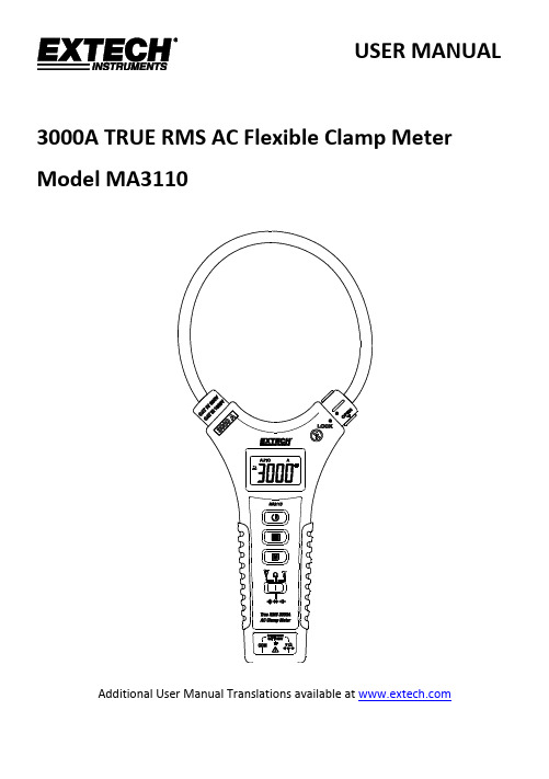
USER MANUAL3000A TRUE RMS AC Flexible Clamp Meter Model MA3110Additional User Manual Translations available at IntroductionThank you for choosing the Extech Model MA3110 Flexible AC Clamp meter with automatic ranging, data hold, and auto power OFF. The MA3110 is a professional CAT III 1000V instrument that measures up to 3000A AC RMS. The MA3110 also measures DC and AC Voltage, Resistance, Capacitance, Diode, and Continuity (beeper). This device is shipped fully tested and calibrated and, with proper use, will provide years of reliable service. Please visit our website() to check for the latest version of this User Guide, Product Updates, Product Registration, and Customer Support.Features∙600A and 3000A AC True RMS Current Measurement ranges∙AC (True RMS) and DC Voltage Measurements∙Automatic ranging∙Meets IEC61010-1, 3rd Edition (2010) CAT III 1000V Safety requirements.∙Resistance, Capacitance, Diode, and Continuity Beeper∙Data Hold feature freezes displayed reading∙6000 count large scale LCD display∙Convenient Flexible Clamp with locking mechanism∙8mm (0.3”) coil diameter for measuring in tight spaces∙Coil length 300mm (11.8“)∙Auto Power OFF after 15 minutes of inactivity∙Overload Protection for most ranges∙Durable, long-lasting components, enclosed in strong, lightweight ABS-plastic housing.Safety InformationTo ensure the safe operation and service of the meter, follow these instructions closely. Failure to observe warnings can result in severe injury.Precautions and Preparations for Measurements∙Ensure that the batteries are connected in the correct polarity and placed in the battery compartment (rear) correctly.∙Place the red and black test leads into the proper input terminals before making measurements.∙Remove the test leads from the circuit under test when changing the measurement ranges. ∙Do not exceed the maximum rated voltage and current on the meter input terminals.∙Remove the battery if the meter is to be stored for long periods∙Replace the test leads only with ones rated for CAT III 1000V or better.∙The meter has an automatic power OFF (APO) utility that switches the meter OFF after 15 minutes of inactivity. Press any key to wake the meter. To disable this feature, press andhold the M (mode) button while switching the meter ON.WarningsWarnings identify hazardous conditions and actions that could cause BODILY HARM or DEATH. ∙Individual protective equipment should be used if HAZARDOUS LIVE parts in the installation where measurements are to be carried out could be accessible.∙If the equipment is used in a manner not specified by the manufacturer, the protection provided by the equipment may be impaired.∙To reduce the risk of fire or electric shock, do not expose this product to rain or moisture.∙Verify the meter operation by measuring a known current. If in doubt, have the meter serviced.∙Do not apply more than the rated voltage/current as marked on the meter.∙To avoid false readings that can lead to electric shock and injury, replace battery as soon as the low battery indicator appears.∙Do not use the meter in or around explosive gas or vapor.∙Do not use a flexible current sensor if the inner copper wire of the flexible cord is visible.∙De-energize the installation under test or wear suitable protective clothing when placing or removing the flexible current probe from a test setup.∙Do not apply/remove the flexible current probe to/from UNINSULATED HAZARDOUS LIVE conductors that may cause electric shock, electric burn, or arc flash.CAUTIONSCAUTIONS identify conditions and actions that could cause DAMAGE to the meter or equipment under test. Do not expose the meter to extremes in temperature or high humidity.Safety Symbols that are typically marked on meters and instructionsCaution: Do not apply voltage or current to the input terminals or clamp thatexceeds the specified rangesCaution: Risk of electric shock!Equipment protected by double or reinforced insulationConforms to EU directivesDo not discard this product in household trash.AC measurementEarth groundPER IEC1010 OVERVOLTAGE INSTALLATION CATEGORYOVERVOLTAGE CATEGORY IEquipment of OVERVOLTAGE CATEGORY I is equipment for connection to circuits in which measures are taken to limit the transient over-voltages to an appropriate low level.Note – Examples include protected electronic circuits.OVERVOLTAGE CATEGORY IIEquipment of OVERVOLTAGE CATEGORY II is energy-consuming equipment to be supplied from the fixed installation.Note – Examples include household, office, and laboratory appliances.OVERVOLTAGE CATEGORY IIIEquipment of OVERVOLTAGE CATEGORY III is equipment in fixed installations.Note – Examples include switches in the fixed installation and some equipment for industrial use with permanent connection to the fixed installation.OVERVOLTAGE CATEGORY IVEquipment of OVERVOLTAGE CATEGORY IV is for use at the origin of the installation.Note – Examples include electricity meters and primary over-current protection equipment.Meter Description1.Flexible Current Clamp2.Clamp Lock Mechanism3.6000-count LCD Display4.Power button5.Data Hold Button6.MODE (M) Button7.Function Switch (-) test lead input terminal9.Positive (+) test lead terminalDisplay IconsH Data HoldAUTO Automatic Range modeAC Alternating CurrentDC Direct CurrentLow battery icon (flashing when measurements cannot be expected to be in-specification)Continuity alert (beeper)V Unit for Voltage measurementsA Unit for Current measurementsΩ, KΩ, MΩUnits for Resistance measurementsnF, uF Units for Capacitance measurementsDiode measurementsOL ‘Overload’ for over range measurements (voltage, current and resistance) - Minus symbol (negative) when the measurement value is negativeMeter PowerThe meter is powered by two (2) 1.5V ‘AALow battery indicationalthough in-specification measurements can still be made temporarily. When the low battery icon begins blinking, in-specification measurements are no longer supported and batteries must be replaced before further measurements can be made. Refer to the battery replacement procedure in the maintenance section.Automatic Power OFFThe meter switches OFF automatically after a 15-minute period of inactivity. To disable the Auto Power OFF feature:∙With the meter power OFF, press and hold the Mode (M) button while powering the meter ON.∙The APO feature is now disabled and the meter will not shut off automatically.∙Note that the next time the meter is powered up, the Auto Power OFF function will be enabled again and the user will have to repeat the Auto Power OFF disable instructionsto disable this function when desired.Data HoldPress the H (HOLD) button with the meter ON to freeze the displayed reading. The H icon will appear along with the held reading. Press the H (HOLD) button again to release the HOLD feature. The H icon will switch OFF and the meter will show real time readings.DC and AC Voltage Measurements1.Connect the black test lead into the COM terminal.2.Connect the red test lead into the ‘V’ terminal.3.4.Put the function switch to the ‘V’ position.5.The display will show the ‘AUTO’ icon (Auto Range mode).6.Press the M (MODE) button to select AC or DC voltage.7.Press the test leads across the circuit under test and read the voltage on the display.8.In the Auto Range mode, the meter will automatically select the optimal range. AC voltagemeasurements are True RMS readings.1.Switch the meter OFF and switch OFF power to the device under test.2.Switch the meter ON and select ‘A’ with the function switch. The display will show theautomatic range icon (AUTO).3.Turn the knurled clamp lock mechanism counter-clockwise to release the flexible clamp.4.Fully enclose only one conductor of the device undertest with the flexible clamp probe (see accompanyingdiagrams). Do not attempt to measure current higherthan the specified current limit.5.Re-lock the clamp turning the clamp lock clockwise.6.Switch power to the device under test ON. Never move fingers above the LCD whenrunning a test.7.Read the current value in the display. The meter will automatically select the appropriaterange (600.0A and 3000A).1.Connect the black test lead into the COM terminal.2.Connect the red t est lead into the ‘Ω’ terminal.3.4.Put the function switch to the ‘Ω’ position.5.The display will show the ‘AUTO’ icon (Auto Range mode).6.Press the M (Mode) button to select resistance Ω mode.7.Press the test leads across the circuit under test and read the resistance on the display.8.In the Auto Range mode, the meter will automatically select the optimal range.CAUTION: Disconnect power to the circuit or device under test when making continuity measurements1.Connect the black test lead into the COM terminal.2.Connect the red test lead into the ‘ohms’ terminal.3.Power the meter using the power button .4.Put the function switch to the ‘ohms’ position.5.The display will show the ‘AUTO’ ico n (Auto Range mode).6.Press the M (Mode) button to select continuity mode.7.The display will show “MANU” icon (Manual Range mode).8.Press the test leads across the circuit under test. The meter will beep and the display willshow the continuity symbol when the resistance is < 20 ohms.Diode MeasurementsCAUTION: Disconnect power to the circuit or device under test when making diode measurements1.Connect the black test lead into the COM terminal.2.Connect the red test lead into the ‘Ω’ terminal.3.Power the meter using the power button .4.Put the function switch to the ‘Ω’ position.5.The display will show the ‘AUTO’ icon (Auto Range mode).6.Press the M (Mode) button to select diode mode. The display will show the manualmode symbol (MANU).7.When connected as shown in test position 1 a forward current flow is established andthe approximate diode forward voltage (VF) value is displayed. If the diode under test isdefective ‘0.000’ (short circuit) or ‘OL’ (open circuit) will display.8.When connected as shown in test position 2 a reverse polarity check is made. If the diodeunder test is good, ‘OL’ will be displayed. If the diode is defective ‘0.000’ or other valueswill be displayed. Proper diode testing should include both polarity measurements.Capacitance MeasurementsCAUTION: Discharge the capacitor under test before taking any capacitance measurements1.Connect the black test lead into the COM terminal.2.Connect the red test lead in to the ‘Ω’ terminal.3.Power the meter using the power button .4.Put the function switch to the ‘Ω’ position.5.The display will show the ‘AUTO’ icon (Auto Range mode).6.Press the M (Mode) button to select the capacitance mo de.7.Press the test leads across the circuit under test and read the capacitance on the display.8.In the Auto Range mode, the meter will automatically select the optimal range.MaintenanceCleaning and StoragePeriodically wipe the case with a damp cloth and mild detergent; do not use abrasives orsolvents. If the meter is not to be used for 60 days or more, remove the batteries and store them separately.Battery Replacement1. Remove the screw that secures the rear battery compartment.2. Remove the battery compartment cover.3. Replace the 2 ‘AAA ’ 1.5V batteries observing correct polarity.4. Re-attach the battery compartment cover.5. Secure the battery compartment with the screw.Never dispose of used batteries or rechargeable batteries in household waste. As consumers, users are legally required to take used batteries to appropriate collection sites, the retail store where the batteries were purchased, or wherever batteries are sold.Disposal: Do not dispose of this instrument in household waste. The user is obligated to take end-of-life devices to a designated collection point for the disposal of electrical and electronic equipment.SpecificationsSpecifications tested under environmental conditions of RF field strength < 3V/M and frequency < 30MHzGENERAL SPECIFICATIONSClamp Flexible type with locking mechanism8mm (0.3”) coil diameter300mm (11.8”) flexible cable lengthDisplay 6000 count LCD with multi-function indicators33.5 x 18.7mm (1.3 x 0.7”) display sizeAuto range 600.0A and 3000A ACSampling rate0.5 to 1 secondLow Battery indication Low voltage display alertsOver-range indication‘OL’ di splayAC bandwidth 50/60Hz (sine wave)AC response True RMSOperating Temperature and Humidity0~50︒C (32~122︒F); 80%RH maximumBattery Two “AA A” 1.5V batteriesBattery consumption 21.1mA approximatelyAuto power OFF After approx. 15 minutes of inactivityDimensions (W x H x D)290 x 135 x 27.8 mm (11.4 x 5.3 x 1.09”)Weight 208g (0.46 lbs.) without batterySafety Standards IEC61010-1, 3rd Edition (2010); Pollution degree 2; Altitude 2000m(6562’) maximum; Indoor use onlyVoltage/Category Rating 1000V CAT III, 600V CAT IVCurrent Rating3000AProbes Listed IEC61010-031 Probes OnlyCopyright © 2016 FLIR Systems, Inc.All rights reserved including the right of reproduction in whole or in part in any formISO-9001 Certified。
瑞士莱姆高精度电流传感器ITZ Ultrastab family
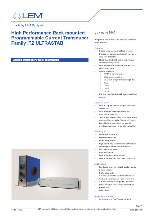
High Performance Rack mounted Programmable Current Transducer Family ITZ ULTRASTABI PM = up to 24kAProgrammable turns ratio optional for some head versionsFeatures · Closed loop (compensated) currenttransducer using an extremely accurate zero flux detector · Electrostatic shield between primaryand secondary circuit · Made up of one measuring head + 19”electronics rack · Heads available:o 600A programmable o 2kA programmableo 2kA non-programmable high BW o 5kA o 10kA o 16kA o 24kA · Custom head configuration available onrequestSpecial features · D-Sub 15 pole female output interfaceconnector · D-Sub 9-pole male status outputinterface connector · Secondary (current) output available onstandard 4mm safety (“banana”) plugs · Full LED indicator panel for status,overload, nominal range etc. indicationAdvantages · Ultrahigh accuracy · Excellent linearity · Wide bandwidth · High immunity to external electrostaticand magnetic fields interference · No insertion losses · High resolution · Low noise on output signal · Low noise feedback to main conductorApplications · Feedback element in high performancepower supplies · Calibration unit · Absolute current standard reference · Test and calibration of current sources · Current extender for power analyzer · Differential current measurement onpower line · MetrologyApplication domain · Industrial and Test/MeasurementGeneric Transducer Family specificationPage 1/2M o d e l U C L E MI n p u t O u t p u t O u t p u t T u r n s R a t i o L i n e a r i t y O f f s e t T c B a n d w i d t h B u s b a r A p e r t u r e +/- A (p k )+/- m A (p k )+/- V (p k )p p m p p m p p m (D C -100H z ) p p m (D C -50k H z )p p m /K+/-3d B / k H z Ø m mN o t e 1)N o t e 2)I T Z 600-S P R T B A 600600600<1<2T B D T B D <0.1>30025.4I T Z 600-S B P R T B A 60010600<3<2T B D T B D <0.6>30025.4I T Z 2000-S P R T B A 200020002000<2<2T B D T B D <0.1>5050I T Z 2000-S B P R T B A 2000102000<4<2T B D T B D <0.6>5050I T Z 2000-S /S P 1T B A 200020001000<2<2T B D T B D <0.1>30050I T Z 2000-S B /S P 1T B A 2000101000<4<2T B D T B D <0.6>30050I T Z 5000-S T B A 500050002500<3<2T B D T B D <0.1>50140I T Z 5000-S B T B A 5000102500<5<2T B D T B D <0.6>50140I T Z 10000-S T B A 10000100005000<5<2T B D T B D <0.1T B D 100I T Z 10000-S B T B A 10000105000<7<2T B D T B D <0.6T B D 100I T Z 16000-S T B A 16000160008000<6<2T B D T B D <0.1T B D 150I T Z 16000-S B T B A 16000108000<8<2T B D T B D <0.6T B D 150I T Z 24000-S T B A 24000240008000<6<2T B D T B D <0.1T B D 150I T Z 24000-S B T B A 24000108000<10<2T B D T B D <0.6T B D 150N o t e s :1) L i n e a r i t y m e a s u r e d a t D C 2) B a n d w i d t h i s m e a s u r e d u n d e r s m a l l s i g n a l c o n d i t i o n s - a m p l i t u d e o f 0.5% I P NN o i se Current Transducer Family ITZ ULTRASTABPage 1/2。
莱姆电子适用于太阳能系统的CTSR系列电流传感器
c om/ ogr Pr amabe Co tol s M ir 80 l— n r l / c o 0 er
Mir 8 0 为M ir 机 器 控 制 系 统 co 0 作 co
功 能 , 既可 作为 P 总 线触 发控 制 器来 完 XI 成P I X 总线 机 箱 内同步 、P I X 总线 多机 箱 同步 ,也 可作 为 频率 源 应用 于P I X 系统 和 ・ P 一3 内 置 高精 度 铷 原 子 钟 作 S3 0
t P 系 统 中 的远程 时 间 同步 、授 时 、频 l Xl  ̄
பைடு நூலகம்
・
P .3 全 面 支 持P 总 线 2 星 S30 XI 槽
的 核 心 部 分 ,结 合 一 体 化 编 程 组 态 软 件
C W ,可 以 同时 对P 4 列变 频 器 ,K3 C F系 / K3 0 服 驱 动 器 和P 人 机 界 面等 元 器 0伺 VC 件进 行编 程组 态 。安装 便利 、维 护方 便 。 结合 中 国 中小 型 机器 市 场 现状 ,
点数 据通 讯 。 作 为Mi o 0 L 不 可 或 缺 的重 要 c 8 0P C r 组 成部 分 ,一 体 化 编程 组 态 软 件C W 遵 C 从I C 6 1 1 程标 准 。易 于获 取 , 安装 E .13 编 简便 。其 标准 版将 免 费提 供 。客 户可 以在 这 个软件 平 台上编 程组 态Mio 0 L S c 80 C n r P 其 他诸 如P 4 列变 频器 和 P C 机 界面 F系 V 人 产 品 ,使用方 便 ,节 约成本 。 基 于罗 克韦 尔 自动 化 和微 软 的V sa i l u Su i 术 , 客 户可 使用C W软件 对P C t o d技 C L
TURCK BIM-IKM-AP6X2-H1141 S34 W KLI3 磁场传感器说明书
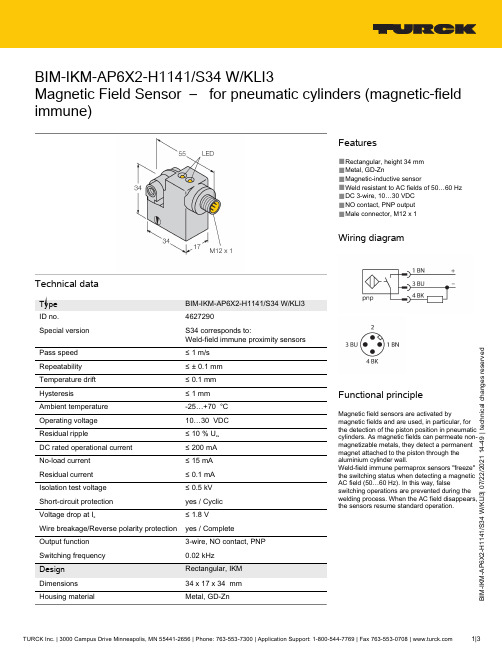
TURCK Inc. | 3000 Campus Drive Minneapolis, MN 55441-2656 | Phone: 763-553-7300 | Application Support: 1-800-544-7769 | Fax 763-553-0708 | 1|3B I M -I K M -A P 6X 2-H 1141/S 34 W /K L I 3 | 07/22/2021 14-49 | t e c h n i c a l c h a n g e s r e s e r v e dBIM-IKM-AP6X2-H1141/S34 W/KLI3Magnetic Field Sensor – for pneumatic cylinders (magnetic-fieldimmune)Technical dataBIM-IKM-AP6X2-H1141/S34 W/KLI34627290S34 corresponds to:Weld-field immune proximity sensors≤ 1 m/s ≤ ± 0.1 mm ≤ 0.1 mm ≤ 1 mm -25…+70 °C 10…30 VDC ≤ 10 % U ss DC rated operational current ≤ 200 mA ≤ 15 mA ≤ 0.1 mA ≤ 0.5 kV yes / Cyclic ≤ 1.8 V Wire breakage/Reverse polarity protection yes / Complete3-wire, NO contact, PNP 0.02 kHz Rectangular, IKM 34 x 17 x 34 mm Metal, GD-ZnFeatures■Rectangular, height 34 mm ■Metal, GD-Zn■Magnetic-inductive sensor■Weld resistant to AC fields of 50…60 Hz ■DC 3-wire, 10…30 VDC ■NO contact, PNP output ■Male connector, M12 x 1Wiring diagramFunctional principleMagnetic field sensors are activated bymagnetic fields and are used, in particular, for the detection of the piston position in pneumatic cylinders. As magnetic fields can permeate non-magnetizable metals, they detect a permanent magnet attached to the piston through the aluminium cylinder wall.Weld-field immune permaprox sensors "freeze"the switching status when detecting a magnetic AC field (50…60 Hz). In this way, falseswitching operations are prevented during the welding process. When the AC field disappears,the sensors resume standard operation.TURCK Inc. | 3000 Campus Drive Minneapolis, MN 55441-2656 | Phone: 763-553-7300 | Application Support: 1-800-544-7769 | Fax 763-553-0708 | 2|3B I M -I K M -A P 6X 2-H 1141/S 34 W /K L I 3 | 07/22/2021 14-49 | t e c h n i c a l c h a n g e s r e s e r v e dTechnical dataMounting instructionsMounting instructions/DescriptionAccessoriesKLI169710Mounting bracket for mounting magnetic field sensors on tie-rodcylinders; cylinder diameter: 32…100mm; material: Die-cast ZincKLI369712Mounting bracket for mounting magnetic field sensors on tie-rodcylinders; cylinder diameter: 63…160mm; material: Die-cast ZincKLI56971802Mounting bracket for mounting magnetic field sensors on profile cylinders; cylinder diameter: 32…50mm; material: AluminumKLI66971805Mounting bracket for mounting magnetic field sensors on profilecylinders; cylinder diameter: 50…100mm; material: AluminumTURCK Inc. | 3000 Campus Drive Minneapolis, MN 55441-2656 | Phone: 763-553-7300 | Application Support: 1-800-544-7769 | Fax 763-553-0708 | 3|3B I M -I K M -A P 6X 2-H 1141/S 34 W /K L I 3 | 07/22/2021 14-49 | t e c h n i c a l c h a n g e s r e s e r v e dKLI76971810Mounting bracket for mounting magnetic field sensors on profilecylinders with external dovetail guide;cylinder diameter: 32…200 mm;material: AluminumKLI5Z 6971803Mounting bracket for mounting magnetic field sensors on tie-rod cylinders; cylinder diameter: 32…63mm; material: AluminumKLI6Z 6971806Mounting bracket for mounting magnetic field sensors on tie-rodcylinders; cylinder diameter: 50…125mm; material: Aluminum。
Silicon Laboratories TS1103系列高侧电流感应器特性、应用和描述说明书

TS1103-200EG6TS1103-25EG6TS1103-50EG6TS1103-100EG6TS1103© 2014 Silicon Laboratories, Inc. All rights reserved.FEATURES♦ Ultra-Low Supply Current: 1μA♦ Wide Input Common Mode Range: +2V to +25V ♦ Low Input Offset Voltage: 200μV (max) ♦ Low Gain Error: 0.6% (max) ♦ Voltage Output♦ Four Gain Options Available:TS1103-25: Gain = 25V/V TS1103-50: Gain = 50V/V TS1103-100: Gain = 100V/V TS1103-200: Gain = 200V/V ♦ 6-Lead SOT23 PackagingAPPLICATIONSNotebook ComputersPower Management SystemsPortable/Battery-Powered Systems Smart Chargers Smart PhonesDESCRIPTIONThe TS1103 is the latest addition to the TS1101 family of bi-directional current-sense amplifiers. Consuming a very low 1μA supply current, the TS1103 high-side current-sense amplifiers combine a 200-µV (max) V OS and a 0.6% (max) gain error for cost-sensitive applications. For all high-side bidirectional current-sensing applications, the TS1103s are self-powered and feature a wide input common-mode voltage range from 2V to 25V. A SIGN comparator digital output is also provided that indicates the direction of current flow depending on the external connections to the TS1103’s RS+ and RS- input terminals.The SOT23 package makes the TS1103 an ideal choice for pcb-area-critical, supply-current-conscious, high-accuracy current-sense applications in all battery-powered and portable instruments.All TS1103s are specified for operation over the -40°C to +105°C extended temperature range.A 1µA, 200µV OS Bidirectional Precision Current-Sense AmplifierTYPICAL APPLICATION CIRCUITSIGN Comparator’s Symmetric I LOAD CrossoverTS1103Page 2TS1103 Rev. 1.0ABSOLUTE MAXIMUM RATINGSRS+, RS- to GND .............................................. -0.3V to +27V V DD , OUT, SIGN to GND ....................................... -0.3V to +6 RS+ to RS- ..................................................................... ±27V Short-Circuit Duration: OUT to GND .................... Continuous Continuous Input Current (Any Pin) ............................ ±20mA Continuous Power Dissipation (T A = +70°C)6-Lead SOT23 (Derate at 4.5mW/°C above +70°C)............................................................................... 360mWOperating Temperature Range .................... -40°C to +105°C Junction Temperature ................................................ +150°C Storage Temperature Range ....................... -65°C to +150°C Lead Temperature (Soldering, 10s) ........................... +300°C Soldering Temperature (Reflow) ............................ +260°CElectrical and thermal stresses beyond those listed under “Absolute Maximum Ratings” may cause permanent damage to the device. These are stress ratings only and functional operation of the device at these or any other condition beyond those indicated in the operational sections of the specifications is not implied. Exposure to any absolute maximum rating conditions for extended periods may affect device reliability and lifetime.PACKAGE/ORDERING INFORMATIONLead-free Program: Silicon Labs supplies only lead-free packaging.Consult Silicon Labs for products specified with wider operating temperature ranges.TS1103TS1103 Rev. 1.0 Page 3ELECTRICAL CHARACTERISTICSV RS+ = 3.6V; V SENSE = (V RS+ - V RS-) = 0V; C OUT = 47nF; V DD = 1.8V; T A = -40°C to +105°C, unless otherwise noted. Typical values are at T A = +25°C. See Note 1.Note 1: All devices are 100% production tested at T A = +25°C. All temperature limits are guaranteed by productcharacterization.Note 2: Extrapolated to V OUT = 0. I CC is the total current into the RS+ and the RS- pins.Note 3: Input offset voltage V OS is extrapolated from a V OUT+ measurement with V SENSE set to +1mV and a V OUT- measurementwith V SENSE set to -1mV; vis-a-viz,Average V OS =(V OUT-) - (V OUT+)2 x GAINNote 4: Amplitude of V SENSE lower or higher than V OS required to cause the comparator to switch output states.Note 5: Gain error applies to current flow in either direction and is calculated by applying two values for V SENSE and thencalculating the error of the actual slope vs. the ideal transfer characteristic: For GAIN = 25, the applied V SENSE is 20mV and 120mV. For GAIN = 50, the applied V SENSE is 10mV and 60mV. For GAIN = 100, the applied V SENSE is 5mV and 30mV. For GAIN = 200, the applied V SENSE is 2.5mV and 15mV.Note 6: The device is stable for any capacitive load at V OUT .Note 7: V OH is the voltage from V RS- to V OUT with V SENSE = 3.6V/GAIN.TS1103Page 4TS1103 Rev. 1.0Input Offset Voltage vs Common-Mode VoltageSupply Current vs Common-Mode Voltage Input Offset Voltage vs TemperatureSupply Current vs TemperatureP E R C E N T O F U N I T S - %INPUT OFFSET VOLTAGE - µV P E R C E N T O F U N I T S - %GAIN ERROR - %I N P U T O F F S E T V O L T A G E - µVTEMPERATURE - °CTEMPERATURE - °CS U P P L Y C U R E N T - µASUPPLY VOLTAGE - Volt5 15 20 20 15 10 01030-10 402V25V3.6VI N P U T O F F S E T V O L T A G E - µVSUPPLY VOLTAGE - VoltS U P P L Y C U R R E N T - µATYPICAL PERFORMANCE CHARACTERISTICSV RS+ = V RS- = 3.6V; T A = +25°C, unless otherwise noted.-40-1510601108551015302510 2050.2 0.6 0.8 0 0.4 1 40 253035-20 0 40 80 -4020 60 -0.4 0.2 -0.6 0.620Input Offset Voltage HistogramGain Error Histogram6030 25 35 30 25 3520510153025200.2 0.6 0.8 00.4 1 -40-151060110853550-0.20.435TS1103TS1103 Rev. 1.0Page 5Gain Error vs Common-Mode Voltage SUPPLY VOLTAGE - Volt Gain Error vs. TemperatureSmall-Signal Gain vs FrequencyS M A L L -S I G N A L G A I N -d BV SENSE - mVC O M M O N -M ODE R E J E C T I O N - d B0.20.30.001 0.111010005-5 -15 -35-25 102030G A I N E R R O R - %G = 100G = 25G = 50G = 100G = 50G = 25V OUT vs V SENSE @ Supply = 3.6VV O U T - VG = 25G = 100G = 50G =25G = 50, 100FREQUENCY - kHz Common-Mode Rejection vs Frequency0.1-0.3-0.20.1 0.2 0.3 -0.1 0 1551501005010060201 2.5 3 3.5 4 1.52 00.20.8 1.0 2 0.4 0.6 0 -10 -20 -30100 0-20 -60-140-80 -40 -100 -120TYPICAL PERFORMANCE CHARACTERISTICSV RS+ = V RS- = 3.6V; T A = +25°C, unless otherwise noted.-40-1535608510TEMPERATURE - °C G A I N E R R O R - %V SENSE - mVV O U T - VV OUT vs V SENSE @ Supply = 2VFREQUENCY - kHz40801.2 1.8 1.4 1.60.5 251100.01 0.001 0.11101000100 0.01 0.4TS1103Page 6TS1103 Rev. 1.0200µs/DIV200µs/DIVSmall-Signal Pulse Response, Gain = 100V S E N S EV O U TV S E N S EV O U TTYPICAL PERFORMANCE CHARACTERISTICSV RS+ = V RS- = 3.6V; C OUT = 0pF; T A = +25°C, unless otherwise noted.200µs/DIV200µs/DIVSmall-Signal Pulse Response, Gain = 50V S E N S EV O U TV S E N S EV O U TLarge-Signal Pulse Response, Gain = 50200µs/DIV200µs/DIVSmall-Signal Pulse Response, Gain = 25V S E N S EV O U TV S E N S E V O U TLarge-Signal Pulse Response, Gain = 25Large-Signal Pulse Response, Gain = 100TS1103TS1103 Rev. 1.0Page 7PIN FUNCTIONSBLOCK DIAGRAMDESCRIPTION OF OPERATIONThe internal configuration of the TS1103 – a bidirectional high-side, current-sense amplifier – is a variation of the TS1100 uni-directional current-sense amplifier. In the design of the TS1103, the input amplifier was reconfiguredfor fully differential input/output operation and a second low-threshold p-channel FET (M2) was added where the drain terminal of M2 is also connected to ROUT. Therefore, the behavior of the TS1103 for when V RS- > V RS+ is identical for when V RS+ > V RS-.Referring to the typical application circuit on Page 1, the inputs of the TS1103’s differential input/output amplifier are connected across an external RSENSE resistor that is used to measure current. At the non-inverting input of the TS1103 (the RS- terminal), the applied voltage is I LOAD x RSENSE. Since the RS- terminal is the non-inverting input of the internal op amp, op amp feedback action forces the inverting input of the internal op amp to the same potential (I LOAD x RSENSE). Therefore, the voltage drop across RSENSE (V SENSE = V RS+ - V RS-) and the voltage drop across RGAINA (at the RS+ terminal) are equal. Necessary for gain ratio match, both RGAINA and RGAINB are the same value.Since p-channel M1’s source is connected to the inverting input of the internal op amp and since the voltage drop across RGAINA is the same as theTS1103 Page 8TS1103 Rev. 1.0external V SENSE, op amp feedback action drives the gate of M1 such that M1’s drain-source current is equal to:I DS(M1)=V SENSE RGAINAorI DS(M1)=I LOAD x R SENSERGAINASince M1’s drain terminal is connected to ROUT, the output voltage of the TS1103 at the OUT terminal is, therefore;V OUT=I LOAD x R SENSE xR OUT RGAINAWhen the voltage at the RS- terminal is greater than the voltage at the RS+ terminal, the external VSENSE voltage drop is impressed upon RGAINB. The voltage drop across RGAINB is then converted into a current by M2 that then produces an output voltage across ROUT. In this design, when M1 is conducting current (V RS+> V RS-), the TS1103’s internal amplifier holds M2 OFF. When M2 is conducting current (V RS-> V RS+), the internal amplifier holds M1 OFF. In either case, the disabled FET does not contribute to the resultant output voltage.The current-sense amplifier’s gain accuracy is therefore the ratio match of ROUT to RGAIN[A/B]. For each of the four gain options available, Table 1 lists the values for ROUT and RGAIN[A/B]. The TS1103’s output stage is protected against input overdrive by use of an output current-limiting circuit of 3mA(typical) and a 7V internal clamp protection circuit.Table 1: Internal Gain Setting Resistors (Typical Values)The SIGN Comparator OutputAs shown in the TS1103’s block diagram, the design of the TS1103 incorporated one additional feature – an analog comparator the inputs of which monitor the internal amplifier’s differential output voltage. While the voltage at the TS1103’s OUT terminal indicates the magnitude of the load current, the TS1103’s SIGN output indicates the load current’s direction. The SIGN output is a logic high when M1 is conducting current (V RS+> V RS-). Alternatively, the SIGN output is a logic low when M2 is conducting current (V RS+< V RS-). The SIGN comparator’s transfer characteristic is illustrated in Figure 1. Unlike other current-sense amplifiers that implement a OUT/SIGN arrangement, the TS1103 exhibits no “dead zone” at I LOAD switchover.Figure 1: TS1103's SIGN Comparator TransferCharacteristic.SIGNPropagationDelay-msFigure 2: SIGN Comparator Propagation Delay vs V SENSE.1000.1101V SENSE (│V RS+ - V RS-│) - mV0.1 1 10 100TS1103TS1103 Rev. 1.0 Page 9The other attribute of the SIGN comparator’s behavior is its propagation delay as a function of applied V SENSE [(V RS+ - V RS-) or (V RS- - V RS+)]. As shown in Figure 2, the SIGN comparator’spropagation delay behavior is symmetric regardless of current-flow direction and is inversely proportional to V SENSE .APPLICATIONS INFORMATIONChoosing the Sense ResistorSelecting the optimal value for the external RSENSE is based on the following criteria and for each commentary follows:1) RSENSE Voltage Loss2) V OUT Swing vs. Applied Input Voltage at V RS+and Desired V SENSE 3) Total I LOAD Accuracy4) Circuit Efficiency and Power Dissipation 5) RSENSE Kelvin Connections1) RSENSE Voltage LossFor lowest IR power dissipation in RSENSE, the smallest usable resistor value for RSENSE should be selected.2) V OUT Swing vs. Applied Input Voltage at V RS+ and Desired V SENSEAs there is no separate power supply pin for the TS1103, the circuit draws its power from the voltage at its RS+ and RS- terminals. Therefore, the signal voltage at the OUT terminal is bounded by the minimum voltage applied at the RS+ terminal.Therefore,V OUT(max) = V RS+(min) - V SENSE(max) – V OH(max) andR SENSE < V OUT (max )GAIN × I LOAD (max )where the full-scale V SENSE should be less than V OUT(MAX)/GAIN at the application’s minimum RS+ terminal voltage. For best performance with a 3.6V power supply, RSENSE should be chosen to generate a V SENSE of: a) 120mV (for the 25V/V GAIN option), b) 60mV (for the 50V/V GAIN option), c) 30mV (for the 100V/V GAIN option), or d) 15mV (for the 200V/V GAIN option) at the full-scale I LOAD current in each application. For the case where the minimum power supply voltage is higher than 3.6V, each of the four full-scale V SENSE s above can be increased.3) Total Load Current Accuracy In the TS1103’s linear region where V OUT < V OUT(max), there are two specifications related to the circuit’s accuracy: a) the TS1103’s input offset voltage (V OS(max) = 200μV) and b) its gain error (GE(max) = 0.6%). An expression for the TS1103’s total error is given by:V OUT = [GAIN x (1 ± GE) x V SENSE ] ± (GAIN x V OS )A large value for RSENSE permits the use of smaller load currents to be measured more accurately because the effects of offset voltages are less significant when compared to larger VSENSE voltages. Due care though should be exercised as previously mentioned with large values of RSENSE.4) Circuit Efficiency and Power DissipationIR losses in RSENSE can be large especially at high load currents. It is important to select the smallest, usable RSENSE value to minimize power dissipation and to keep the physical size of RSENSE small. If the external RSENSE is allowed to dissipate significant power, then its inherent temperature coefficient may alter its design center value, thereby reducing load current measurement accuracy. Precisely because the TS1103’s input stage was designed to exhibit a very low input offset voltage, small RSENSE values can be used to reduce power dissipation and minimize local hot spots on the pcb.5) RSENSE Kelvin ConnectionsFor optimal V SENSE accuracy in the presence of large load currents, parasitic pcb track resistance should be minimized. Kelvin-sense pcb connections between RSENSE and the TS1103’s RS+ and RS- terminals are strongly recommended. The drawing in Figure 3 illustrates the connections between theTS1103Page 10TS1103 Rev. 1.0current-sense amplifier and the current-sense resistor. The pcb layout should be balanced and symmetrical to minimize wiring-induced errors. In addition, the pcb layout for RSENSE should include good thermal management techniques for optimal RSENSE power dissipation.6) RSENSE CompositionCurrent-shunt resistors are available in metal film, metal strip, and wire-wound constructions. Wire-wound current-shunt resistors are constructed with wire spirally wound onto a core. As a result, these types of current shunt resistors exhibit the largest self inductance. In applications where the load current contains high-frequency transients, metal film or metal strip current sense resistors are recommended.Internal Noise FilterIn power management and motor control applications, current-sense amplifiers are required to measure load currents accurately in the presence of both externally-generated differential and common-mode noise. An example of differential-mode noise that can appear at the inputs of a current-sense amplifier is high-frequency ripple. High-frequency ripple – whether injected into the circuit inductively or capacitively - can produce a differential-mode voltage drop across the external current-shunt resistor (RSENSE). An example of externally-generated, common-mode noise is the high-frequency output ripple of a switching regulator that can result in common-mode noise injection into both inputs of a current-sense amplifier.Even though the load current signal bandwidth is DC, the input stage of any current-sense amplifier can rectify unwanted, out-of-band noise that can result in an apparent error voltage at its output. This rectification of noise signals occurs because all amplifier input stages are constructed with transistors that can behave as high-frequency signal detectors in the same way pn-junction diodes were used as RF envelope detectors in early radio designs. Against common-mode injected noise, the amplifier’s internal common-mode rejection is usually sufficient.To counter the effects of externally-injected noise, it has always been good engineering practice to add external low-pass filters in series with the inputs of a current-sense amplifier. In the design of discrete current-sense amplifiers, resistors used in the external low-pass filters were incorporated into the circuit’s overall design so errors because of any input-bias current-generated offset voltage errors and gain errors were compensated.With the advent of monolithic current-sense amplifiers, like the TS1103, the addition of external low-pass filters in series with the current-sense amplifier’s inputs only introduces additional offset voltage and gain errors. To minimize or eliminate altogether the need for external low-pass filters and to maintain low input offset voltage and gain errors, the TS1103 incorporates a 50-kHz (typ), 2nd -order differential low-pass filter as shown in the TS1103’s Block Diagram.Output Filter CapacitorIf the TS1103 is part of a signal acquisition system where its OUT terminal is connected to the input of an ADC with an internal, switched-capacitor track-and-hold circuit, the internal track-and-hold’s sampling capacitor can cause voltage droop at V OUT . A 22nF to 100nF good-quality ceramic capacitor from the OUT terminal to GND forms a low-pass filter with the TS1103’s R OUT and should be used to minimize voltage droop (holding V OUT constant during the sample interval. Using a capacitor on the OUT terminal will also reduce the TS1103’s small-signal bandwidth as well as band-limiting amplifier noise.PC Board Layout and Power-Supply Bypassing For optimal circuit performance, the TS1103 should be in very close proximity to the external current-sense resistor and the pcb tracks from RSENSE to the RS+ and the RS- input terminals of the TS1103 should be short and symmetric. Also recommended are a ground plane and surface mount resistors and capacitors.Figure 3: Making PCB Connections to RSENSE.TS1103400 West Cesar Chavez, Austin, TX 78701TS1103 Rev. 1.0+1 (512) 416-8500 ▪ PACKAGE OUTLINE DRAWING6-Pin SOT23 Package Outline Drawing(N.B., Drawings are not to scale)Note:Dimension are exclusive of mold flash and gate burr.2. Dimension are exclusive of solder plating.2.80 -3.00TS1103-200EG6TS1103-25EG6TS1103-50EG6TS1103-100EG6。
纳芯微-NSM2012 高精度霍尔电流传感器 数据手册说明书

NSM2012 基于霍尔原理,高精度,具有共模磁场抑制,可达3000V隔离的电流传感器Datasheet (CN) 1.0Product OverviewNSM2012是一款集成路径电流传感器,具有1.2mΩ极低的导通电阻,减少了芯片上的热损耗。
纳芯微创新的隔离技术以及信号调理设计能够满足高隔离等级的同时感测流过内部B usbar的电流。
内部采用差分霍尔对,因此对外部杂散磁场有很强的抵御能力。
NSM2012支持比例输出和固定输出模式,固定模式方便客户ADC差分采样Vref以及Vout的电压以减少外部共模干扰(比如温度等)。
对比同样Shunt+隔离运放的电流采样方式,NSM2012省去了原边供电并且Layout简单方便,同时具有极高隔离耐压以及Lifetime稳定性。
在高边电流检测应用中只需用一颗NSM2012即可达到600V pk工作电压,无需加任何保护器件即可耐受6kV浪涌电压。
由于NSM2012内部精确的温度补偿算法以及出厂精度校准,此电流传感器在全温度工作范围都可以保持很好的精度,客户无需做二次编程。
支持3.3V/5V供电电压(不同供电版本)。
Key Features•高带宽以及快速响应时间•400kHz带宽• 1.5us响应时间•高精度电流测量•差分霍尔检测可抵御外界杂散磁场•满足UL标准的高隔离等级•耐受隔离耐压(V ISO):3000Vrms•最大浪涌隔离耐压(V surge):6kV•CMTI > 100V/ns•CTI(I)•爬电距离/电气间距:4mm•纳芯微创新的斩波以及旋转电流激励技术使得零点温漂很小•比例输出或者固定输出•工作温度:-40℃ ~ 125℃•原边导通电阻:1.2mΩ•SOIC8封装•满足UL62368/EN62368安规认证•ROHSApplications•光伏•工业电源•电机控制•OBC/DCDC/PTC Heater•充电桩Device InformationFunctional Block DiagramsFigure 1. NSM2012 Block DiagramINDEX1. PIN CONFIGURATION AND FUNCTIONS (3)2. ABSOLUTE MAXIMUM RATINGS (4)3. ISOLATION CHARACTERISTICS (4)4. SPECIFICATIONS (5)4.1C OMMON C HARACTERISTICS (TA=-40°C TO 125°C,VCC=5V OR 3.3V, UNLESS OTHERWISE SPECIFIED) (5)4.2NSM2012-30B3R-DSPR C HARACTERISTICS (TA=-40°C TO 125°C,VCC=3.3V, UNLESS OTHERWISE SPECIFIED) (6)4.3NSM2012-30B5R-DSPR C HARACTERISTICS (TA=-40°C TO 125°C,VCC=5V, UNLESS OTHERWISE SPECIFIED) (6)4.4NSM2012-10U5R-DSPR C HARACTERISTICS (TA=-40°C TO 125°C,VCC=5V, UNLESS OTHERWISE SPECIFIED) (7)4.5NSM2012-20B5R-DSPR C HARACTERISTICS (TA=-40°C TO 125°C,VCC=5V, UNLESS OTHERWISE SPECIFIED) (8)4.6T YPICAL P ERFORMANCE C HARACTERISTICS (9)NSM2012-30B3R-DSPR[1] (9)NSM2012-30B5R-DSPR[1] (9)NSM2012-10U5R-DSPR[1] (10)NSM2012-20B5R-DSPR[1] (11)5. FUNCTION DESCRIPTION (13)5.1.O VERVIEW (13)5.2.NSM2012R版本(单端比例输出) (13)5.3.NSM2012F版本(固定输出版本) (13)5.4.NSM2012专业术语定义 (13)6. APPLICATION NOTE (16)6.1.典型应用电路 (16)6.2.PCB L AYOUT (16)6.3.热评估实验 (17)7. PACKAGE INFORMATION (18)8. ORDER INFORMATION (19)9. TAPE AND REEL INFORMATION (20)10. REVISION HISTORY (21)1. Pin Configuration and FunctionsR Version F VersionFigure 1.1 NSM2012 PackageTable 1.1 NSM2012 Pin Configuration and Description2.Absolute Maximum Ratings3.Isolation Characteristics4.Specifications[1]: 被设计保证。
莱姆推出新型电流传感器 精确测量高达4000A
莱姆推出新型电流传感器精确测量高达4000A
佚名
【期刊名称】《《可编程控制器与工厂自动化(PLC FA)》》
【年(卷),期】2009(000)006
【摘要】近日,世界领先的电流与电压测量元器件制造商LEM电子在北京推出ITL4000S电流传感器,用于对高达268mm直径导体内高达4000ARMS的电流进行无创伤性测量。
该新型传感器使得在高达50kHz(+/-1dB)频率下交流电流、直流电流和脉冲电流的隔离测量达到峰值测量标称值的三倍。
【总页数】1页(P21)
【正文语种】中文
【中图分类】TP212
【相关文献】
1.莱姆采用新一代磁通门技术推出低噪声、宽温度范围的高精度电流传感器 [J], ;
2.莱姆电子发布全新品牌,推出三类电流传感器 [J], 鲁冰
3.莱姆推出LFxx10系列电流传感器 [J],
4.莱姆推出新型HO6/10/25-P系列电流传感器 [J], 郭超
5.R&S推出业界首款内置衰减器的新型倍频器SMZ,精确调整输出电平,频率高达110GHz [J],
因版权原因,仅展示原文概要,查看原文内容请购买。
- 1、下载文档前请自行甄别文档内容的完整性,平台不提供额外的编辑、内容补充、找答案等附加服务。
- 2、"仅部分预览"的文档,不可在线预览部分如存在完整性等问题,可反馈申请退款(可完整预览的文档不适用该条件!)。
- 3、如文档侵犯您的权益,请联系客服反馈,我们会尽快为您处理(人工客服工作时间:9:00-18:30)。
High Performance Rack mounted Programmable Current Transducer Family ITZ ULTRASTAB
I PM = up to 24kA
Programmable turns ratio optional for some head versions
Features · Closed loop (compensated) current
transducer using an extremely accurate zero flux detector · Electrostatic shield between primary
and secondary circuit · Made up of one measuring head + 19”
electronics rack · Heads available:
o 600A programmable o 2kA programmable
o 2kA non-programmable high BW o 5kA o 10kA o 16kA o 24kA · Custom head configuration available on
request
Special features · D-Sub 15 pole female output interface
connector · D-Sub 9-pole male status output
interface connector · Secondary (current) output available on
standard 4mm safety (“banana”) plugs · Full LED indicator panel for status,
overload, nominal range etc. indication
Advantages · Ultrahigh accuracy · Excellent linearity · Wide bandwidth · High immunity to external electrostatic
and magnetic fields interference · No insertion losses · High resolution · Low noise on output signal · Low noise feedback to main conductor
Applications · Feedback element in high performance
power supplies · Calibration unit · Absolute current standard reference · Test and calibration of current sources · Current extender for power analyzer · Differential current measurement on
power line · Metrology
Application domain · Industrial and Test/Measurement
Generic Transducer Family specification
Page 1/2
M o d e l U C L E M
I n p u t O u t p u t O u t p u t T u r n s R a t i o L i n e a r i t y O f f s e t T c B a n d w i d t h B u s b a r A p e r t u r e +/- A (p k )+/- m A (p k )+/- V (p k )
p p m p p m p p m (D C -100H z ) p p m (D C -50k H z )p p m /K
+/-3d B / k H z Ø m m
N o t e 1)
N o t e 2)
I T Z 600-S P R T B A 600600600<1<2T B D T B D <0.1>30025.4I T Z 600-S B P R T B A 60010
600<3<2T B D T B D <0.6>30025.4I T Z 2000-S P R T B A 20002000
2000<2<2T B D T B D <0.1>5050I T Z 2000-S B P R T B A 200010
2000<4<2T B D T B D <0.6>5050I T Z 2000-S /S P 1T B A 20002000
1000<2<2T B D T B D <0.1>30050I T Z 2000-S B /S P 1T B A 200010
1000<4<2T B D T B D <0.6>30050I T Z 5000-S T B A 50005000
2500<3<2T B D T B D <0.1>50140I T Z 5000-S B T B A 500010
2500<5<2T B D T B D <0.6>50140I T Z 10000-S T B A 1000010000
5000<5<2T B D T B D <0.1T B D 100I T Z 10000-S B T B A 1000010
5000<7<2T B D T B D <0.6T B D 100I T Z 16000-S T B A 1600016000
8000<6<2T B D T B D <0.1T B D 150I T Z 16000-S B T B A 1600010
8000<8<2T B D T B D <0.6T B D 150I T Z 24000-S T B A 2400024000
8000<6<2T B D T B D <0.1T B D 150I T Z 24000-S B T B A 24000
10
8000<10<2T B D T B D <0.6T B D 150
N o t e s :1) L i n e a r i t y m e a s u r e d a t D C 2) B a n d w i d t h i s m e a s u r e d u n d e r s m a l l s i g n a l c o n d i t i o n s - a m p l i t u d e o f 0.5% I P N
N o i s
e Current Transducer Family ITZ ULTRASTAB
Page 1/2。