G104XVN01.0 友达10.4寸全视角宽温工业液晶屏-杭州旭虹科技有限公司
友达5.7寸液晶屏G057VTN01 V0规格书-杭州旭虹科技有限公司

G057VTN01 V0 Color TFT-LCD Module5.7” VGA Landscape LED BacklightWide Temperature Range Mercury-free solution RoHS and Halogen-freeComplianceHigh Shock/Vibration Resistance Outline and Interface are fullycompatible with G057VN01 serials(Preliminary)Size (inch)5.7” ModelG057VN01 V210 Resolution (pixel) 640(RGB) x 480 Active Area (mm) 115.2(H) x 86.4(V)Pixel Pitch (mm) 0.18 x 0.18Mode TNLCD Surface Anti-Glare, Hardness 3HNumber of Colors 262K View Angle (L/R/U/D) 80/80/70/70 (typ.) Brightness(nit) (25℃) 500(min.), 600 (typ.)Contrast Ratio (25℃) 800:1 (typ.) Response Time (ms) 25 (typ.) LED Life (hrs.)50K Power Consumption (W) 3.74W Supply Voltage (V) 3.3V Storage Temp. (℃) -30 ~ 85 Operation Temp. (℃) -30 ~ 85Outline Dimension (mm) 144.0(H) x 104.6(V) x12.3(D) (typ.) Weight (g) 150g (typ.), 165g (max.)InterfaceCMOSTFT- LCD Interface Signal Description:Note 1: “Low” stands for 0V. “High” stands for 3.3V. “NC” stands for ”No Connection”.TFT- LCD Signal (CN1): LCD Connector: ManufacturerStarconnConnector Model Number 089H33-000100-G2-R, compatible withIMSA-9637S-33Y902 & ELCO 08-6210--033-340-800+Pin# Symbol Pin# Symbol Pin# Symbol 1 GND 12 GND 23 B3 2 DOTCLK 13 G0 24 B4 3 NC 14 G1 25 B5 4 NC 15 G2 26 GND 5 GND 16 G3 27 DE 6 R0 17 G4 28 VDD 7 R1 18 G5 29 VDD 8 R2 19 GND 30 R/L 9 R3 20 B0 31 U/D 10 R4 21 B1 32 NC 11 R522B233GNDLED Backlight Unit (CN2): Backlight Connector:ManufacturerJSTConnector Model Number SM06B-SRKS-G-TBcompatible with JST SM06B-SRSS-TB (LS) (SN)Mating Connecter Model Number JST SHR-06V-BKHF-B or compatiblePin # Symbol Pin # Symbol 1 V LED 4 GND 2 V LED 5 PWM DIM 3GND6LED ON/OFFLED Light Bar Input (CN3): Light Bar Connector ManufacturerSTM or compatible Connector Model Number P24021P6 or compatible Mating Connecter Model NumberSM06B-SHLS-TF or compatiblePin # Symbol Pin Description Cable color1 AN1 Channel 1 LED anode Red2 AN2 Channel 2 LED anode Red3 AN3 Channel 3 LED anode Red4 CA1 Channel 1 LED cathode White5 CA2 Channel 2 LED cathode Blue6 CA3Channel 3 LED cathodeBlack工业液晶屏www.hzxuhong.comReliability Test Criteria: ItemsRequired Condition Remark Temperature Humidity Bias40℃/90%,300HrNote 2 High Temperature Operation 85℃,300Hr Note 2 Low Temperature Operation -30℃,300Hr Note 2 High Temperature Storage 85℃,300 hours Note 2 Low Temperature Storage -30℃,300 hoursNote 2 Thermal Shock Test -20℃/30 min ,60℃/30 min ,100cyclesNote 2 Hot Start Test 85℃/1 Hr (min.), power on/off per 5 minutes, repeat 5 times Note 2 Cold Start Test -30℃/1 Hr (min.), power on/off per 5 minutes, repeat 5 times Note 2 Shock Test (Non-Operating) 50G, 20ms,Half-sine wave, (±X, ±Y , ±Z)Note 2Vibration Test (Non-Operating)(1)Random Wave 3.3rms, 0.5hr(X,Y,Z), 5~500hz (2)Sine Wave 6.8G, 10~400hz, 4hr40min (XYZ)Note 2ESDContact Discharge: ±8KV, 150pF(330Ω) 1sec, 8 points, 25times/pointAir Discharge: ±15KV, 150pF(330Ω) 1sec, 8 points, 25 times/pointNote 1,2Attitude TestOperating: 14,000 ft, Ramp: 2000 ft/min, 8hrs Non-operating: 40,000 ft, Ramp: 2000 ft/min, 24hrsNote 2Note1: According to EN61000-4-2 ESD class B criteria, some performance degradation is allowed. TFT-LCD module is self-recoverable, no data lost and no hardware failures after test. Note2:Water condensation is not allowed for each test items.Each test is done by new TFT-LCD module. Don’t use the same TFT-LCD module repeatedly for reliability test.The reliability test is performed only to examine the TFT-LCD module capability.To inspect TFT-LCD module after reliability test, please store it at room temperature and room humidity for 24 hours at least in advance.工业液晶屏www.hzxuhong.comVersion 0.2, Mar 2012Mechanical Characteristics:工业液晶屏www.hzxuhong.com。
C103VAN01.1规格书Product Spec_v02_20160127-杭州旭虹科技有限公司
Model Name:
Planned Lifetime: Phase-out Control: EOL Schedule:
< From
C103VAN01.1
2016/Jan To 2019/Dec From 2019/Apr To 2019/Dec 2019/Apr
工业液晶屏http://www.hzxuhong.com
杭州旭虹科技有限公司
C. Physical Specifications
F. G. H.
Optical specifications (Note 1, 2) ................................................................................ 20 Reliability Test Items (Note 2)...................................................................................... 22 Packing Form................................................................................................................ 23
杭州旭虹科技有限公司
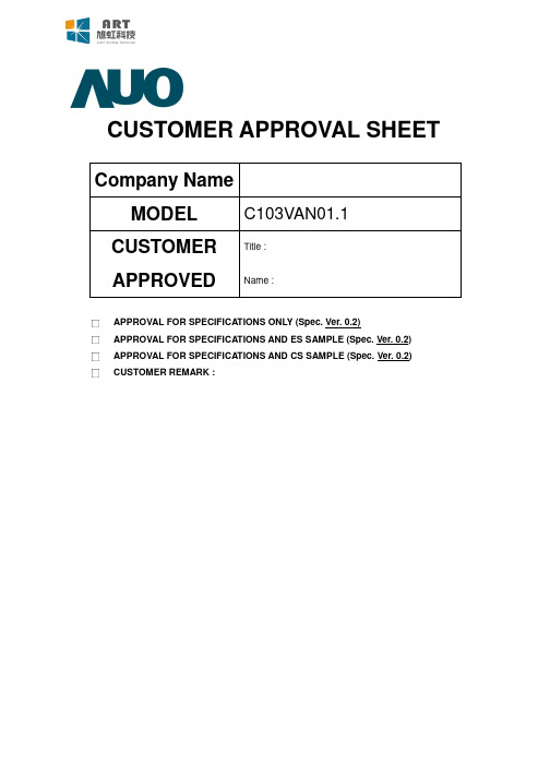
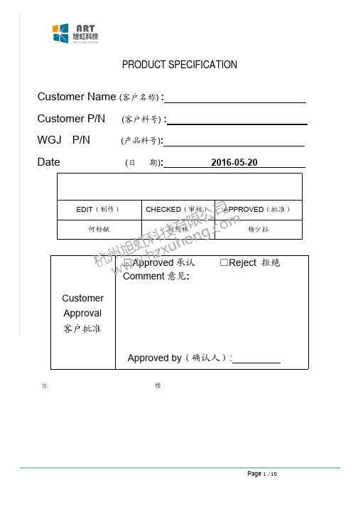
CUSTOMER APPROVAL SHEET
Company Name MODEL CUSTOMER APPROVED
□ □ □ □
C103VAN01.1
Title :
Name :
APPROVAL FOR SPECIFICATIONS ONLY (Spec. Ver. 0.2) APPROVAL FOR SPECIFICATIONS AND ES SAMPLE (Spec. Ver. 0.2) APPROVAL FOR SPECIFICATIONS AND CS SAMPLE (Spec. Ver. 0.2) CUSTOMER REMARK :
京东方10.4寸BA104S01-200规格书-杭州旭虹科技

SpecificationForApproval■Preliminary specification□ Final specificationTitle 10.4SVGA(PS) TFT-LCD (Module)BuyerModelSupplier Cheng Du BOE Optoelectronics Technology CO., LTDModelTITLE/SIGNATURE DATE ITEM SIGNATURE/DATEApprovedReviewedReviewedPreparedPlease return one copy confirmation with signature and your commentsBOE CHENG DU Optoelectronics Technology CO., LTDCONTENT LISTCover ----------------------------------------------------------------------------------------------1 Content List---------------------------------------------------------------------------------------2 Record of Revisions-----------------------------------------------------------------------------31. General Description--------------------------------------------------------------------------42. Electrical Specifications ---------------------------------------------------------------------63. Signal Timing Specification-----------------------------------------------------------------------124. Interface Connection------------------------------------------------------------------------------155. Optical Specifications ----------------------------------------------------------------------176. Mechanical Characteristics ----------------------------------------------------------------207. Reliability Test ------------------------------------------------------------------------------238. Packing Method ----------------------------------------------------------------------------249. Product ID Rule ----------------------------------------------------------------------------2510. Handling & Cautions ---------------------------------------------------------------------2711. Applicable Scope ---------------------------------------------------------------------------------29Record of RevisionsRevision Date Page Description Released by Pre.0 2014.09.09 Initial Released Huangli Pre.1 2014.10.30 Update revision: Revise clerical error Huangli1.0 GENERAL DESCRIPTION1.1 Introduction10.4SVGA is a color active matrix TFT-LCD panel using amorphous silicon TFT's (Thin Film Transistors) as an active switching devices. This model is composed of a TFT-LCD Panel, a driving circuit and a back light system. It is a transmissive type display operating in the normal white. This TFT-LCD has a 10.4 inch diagonally measured active area with SVGA resolutions (800 horizontal by 600 vertical pixel array). Each pixel is divided into Red, Green, Blue dots which are arranged in vertical stripe and this panel can display 16.7M Dithering (RGB 8-Bits) or 262K colors (RGB 6-bits).10.4” SVGA800*RGB*6001.2 Features● 0.5t Glass (Single)● Module Design● Low power consumption● Thin and light weight● High luminance and contrast ratio, low reflection and wide viewing angle● RoHS Compliant1.3 Application● Medical & Industrial application1.4 General Specifications (H: horizontal length, V: vertical length)Parameter Specification Unit Remark Active Area 211.2(H) × 158.4(V) mmNumber of Pixels 800(H) RGB × 600(V) pixelsPixel Pitch 0.264(H) × 0.264(V) mmPixel Arrangement RGB Vertical stripeDisplay Colors 262K /16.7M Dithering color colorsColor Gamut 50%(typ.)Display Mode Normally white, Transmissive modeDimensional Outline 236(H) × 176.9(V) × 5.6(D) mmBacklight Top edge side, 1-LED Lighting BarTypePolarizer surface treatment Haze 25%(CF)/ Clear(TFT)Polarizer compensationWide viewtypeViewing Direction12 o’clock Note 1,2 (Human Eye)D-IC HX8245(Source)+HX8677(Gate)Weight 288g (typ.) gramNote:1.The biggest CR Direction: 6 O’clock, The worst Gray Inversion direction: 6 O’clock.2.The TFT and CF Rubbing DirectionGray Inversion angle3. This product’s compatible IC is HX8245 (Source) + HX8677(Gate), Please contact IC manufacturer and verify it when you choose any one of them. The information we suppose about IC just for reference.2.0 ELECTRICAL SPECIFICATION2.1 Absolute Maximum RatingsThe followings are maximum values which, if exceed, may cause faulty operation or damage to the unit. The operational and non-operational maximum voltage andcurrent values are listed in Table below.Parameter Symbol Min. Typ. Max. Unit Remark Power Supply VoltageV DD 3.0 3.3 3.6 V (LCD Module)Back-light Power SupplyHV DD17.7 20.7 VVoltageBack-light LED Current I LED30 mAOperating Temperature T OP-20 +70 ℃Note Storage Temperature T ST-30 +80 ℃Note:Temperature and relative humidity range are shown in the Figure below.Wet bulb temperature should be 39℃ max. and no condensation of water.2.2 Electrical specificationParameter Symbol Values Unit Note Min. Typ.Max. Power Supply InputVoltage VDD 3.0 3.3 3.6 V Power Supply Current IDD 480 mA Back-light Power Supply Voltage HVDD 20.7 V Back-light Power Supply Current IHVDD 120 mA 4 parallel * 6string Positive-going Input Threshold Voltage VIT+ +100 mV Vcom = 1.2V( typ.) Negative-going Input Threshold Voltage VIT- -100 mV Differential input common mode voltage Vcom 1.2 V VIH=100mV, VIL=-100mV Power ConsumptionPD 1.6 W Note 1 PBL 2.484 W Note 2 PTotal4.084W2.3 Backlight Driving ConditionsNotes:1. Calculator Value for reference I LED ×V LED ×LED Quantity = P LED2. The LED Life-time define as the estimated time to 50% degradation of initial luminous.Parameter SymbolMin Typ Max Unit RemarkLED Forward Voltage VF 17.4 19.2 20.4 V - LED Forward CurrentIF - 30 - mA - LED Power Consumption PLED 2.09 2.31 2.45 W Note 1 LED Life-Time N/A-30,000-HrsIF = 30mA Note 22.4 Block Diagram2.5 INPUT SIGNALS, BASIC DISPLAY COLORS & GRAY SCALE OF COLORS2.6 Power Sequence2.7 FPC Schematic3.0 SIGNAL TIMING SPECIFICATION3.1 The BA104S01-200 is operated by the DE only.DE mode (800 x 600)3.2 LVDS Rx Interface Timing ParameterThe specification of the LVDS Rx interface timing parameter is shown below.ParameterSymbol Min Typ Max Unit DCLK Frequency fclk 32.6 39.6 62.4 MHz Horizontal Display Areathd 800 DCLK HSD Period th 900 1056 1300 DCLK HSD Blanking thb + thfp90 200 500 DCLK Vertical Display Areatvd 600 TH VSD Period tv610 630 800 TH VSD Blankingtvbp + tvfp1030200THParameterSymbol Min Typ Max Unit ConditionClock frequency RXFCLK 20 - 85 MHz -Input data skewmargin TRSKM -600 -+600 pS | VID | =200mV RXVCM =1.2V RXFCLK =65MHzClock high time TLVCH - 4/(7* RXFCLK) - ns - Clock low time TLVCL - 3/(7* RXFCLK)- ns - PLL wake-up timeTemPLL--150μs-LVDS mode AD electrical characteristics3.3 Signal timing waveforms of Interface Signala. Input Clock and Data Timing Diagramb. Source Output Timing DiagramSource output timing diagramOutput load condition4.0 INTERFACE CONNECTION4.1 Electrical Interface ConnectionThe electronics interface connector is STM MSB24013P20 or compatible. The connector interface pin assignments are listed below.Pin Symbol Function1 VDD Logic Power 3.3V (Panel logic)2 VDD Logic Power 3.3V (Panel logic)3 GND Ground4 GND Ground5 IN0- LVDS receiver negative signal channel 06 IN0+ LVDS receiver positive signal channel 07 GND Ground8 IN1- LVDS receiver negative signal channel 19 IN1+ LVDS receiver positive signal channel 110 GND Ground11 IN2- LVDS receiver negative signal channel 212 IN2+ LVDS receiver positive signal channel 213 GND Ground14 CLK- LVDS receiver negative signal clock15 CLK+ LVDS receiver positive signal clock16 GND Ground17 IN3- LVDS receiver negative signal channel 3(NC for 6bit LVDS input)18 IN3+ LVDS receiver positive signal channel 3(NC for 6bit LVDS input)19 GND Ground20 SEL68 6/8bits LVDS data input selection [H:8bit L/NC:6bit]Note 1: High stands for “2.7--3.3V”, Low stands for “0--0.4”.4.2 LVDS Input signal 4.3 Data Input Format5.0 OPTICAL SPECIFICATIONS5.1 OverviewThe test of Optical specifications shall be measured in a dark room (ambient luminance≤ 1 lux and temperature = 25±2℃) with the equipment of Luminance meter system (Topcon SR-UL1R and Westar TRD-100A) and test unit shall be located at an approximate distance 50cm from the LCD surface at a viewing angle of θ and Φ equal to 0°.The center of the measuring spot on the Display surface shall stay fixed.The backlight should be operating for 30 minutes prior to measurement. Optimum viewing angle direction is 12 o’clock. 5.2 Optical SpecificationsNote:1. Viewing angle is the angle at which the contrast ratio is greater than 10. The viewing are determined for the horizontal or 3, 9 o’clock direction and the vertical or 6, 12 o’clock direction with respect to the optical axis which is normal to the LCD surface (see FIG.2).2. Contrast measurements shall be made at viewing angle of Θ= 0 and at the center of the LCD surface. Luminance shall be measured with all pixels in the view field set first to white, then to the dark (black) state. (See FIG. 2) Luminance Contrast Ratio (CR) is defined mathematically.Parameter Symbol Condition Min. Typ. Max. UnitRemark Threshold Voltage Vsat 2.0 2.2 2.4 V Fig.1Vth 1.1 1.3 1.5 V Viewing AngleHorizontal Θ3 CR>10 60 70 ° Note 1 Θ9 60 70 ° VerticalΘ12 50 60 ° Θ6 60 70 °Contrast Ratio CR Θ= 0° 600 800 Note 2 Luminance cd/m2Θ= 0° 250 300 lm Note 3 Uniformity%Θ= 0° 70% 80% Note 4 NTSC% Θ= 0°50%Reproduction Of colorRedRx Θ= 0°TBD Note 5 *ModuleRy TBD Green Gx TBD Gy TBD BlueBx TBD By TBD White Wx Θ= 0° TBD WyTBDResponse Time Tr+TfΘ= 0°30ms Note 6CR = Luminance when displaying a white raster Luminance when displaying a black raster3. Surface luminance is the center point across the LCD surface 50cm from the surface with all pixels displaying white. This measurement shall be taken at the locations shown in FIG. 2.4. Uniformity measurement shall be taken at the locations shown in FIG. 2&3, for a total of the measurements per display, measure surface luminance of these nine points across the LCD surface 50cm from the surface with all pixels displaying white.Uniformity = Min Luminance of 9 points×100% Max Luminance of 9 points5. The color chromaticity coordinates specified in Table1 shall be calculated from The spectral data measured with all pixels first in red, green, blue and white. Measurements shall be made at the center of the Module.6. The electro-optical response time measurements shall be made as FIG.4 by switching the “data” input signal ON and OFF.The times needed for the luminance to change from 10% to 90% is Tr and 90% to 10% is Tf. Figure 1. The definition of Vth & VsatFigure 2. Measurement Set Up(L = 50cm)Figure 3. Uniformity Measurement LocationsFigure 4. Response Time Testing ColumnRow6.0 MECHANICAL CHARACTERISTICS6.1 Dimension RequirementsMechanical outlines for the panel (H: horizontal length, V: vertical length )Note:The size specified is calculated by IC –driver HX8245(Source) + HX8677(Gate), the size maybe changed if customer use other IC.Parameter Specification Unit RemarkPanel size 221.6(H) × 171(V) mm CF size 218.4(H) × 165.4(V) mm Active area 211.2(H) × 158.4(V) mm Number of pixels 800(H)RGB × 600(V) pixels(1 pixel = R + G + B dots) Pixel pitch 0.264(H) × 0.264(V) mm Pixel arrangement RGB Vertical stripePanel ID 10 × 2mm COG pad area 5.6(Source), 3.2(Gate)mm D-IC to FPC distance 0.5(Source) mm Note D-IC width 1.07(Source), 0.67(Gate) mm D-IC to CF edge 2.83(Source), 1.87(Gate)mm FPC to Glass edge 0.3(Source) mmFPC width0.9(Source) mmSeal Area (U/D/L/R) 3.5/3.5/3.6/3.6 mm Dimensional outline 236(H) × 176.9(V) × 5.6(D)mm Display modeNormally whiteFigure 5. LCM Outline Dimension (unit:mm)Figure 6. FPC main structure (unit:mm)FPCA100±20um113±20um20±5u m0.085±0.020.45±0.150.45±0.150.4501.00±0.03pitch:0.20±0.031m m M a xspace:0.10±0.03width:0.10±0.03width:0.15±0.02space:0.15±0.022-R 0.250.80±0.031.10±0.154-0.80±0.030.502-2.814-0.20±0.030.30±0.023.00±0.201.48±0.20FPCB3.00±0.201.48±0.200.30±0.024-0.20±0.032-1.500.504-0.80±0.031.10±0.150.80±0.032-R 0.25space:0.15±0.02width:0.15±0.02width:0.10±0.03space:0.10±0.031m m M a xpitch:0.20±0.031.00±0.030.4500.45±0.150.45±0.150.085±0.0220±5u m113±20um100±20um7.0 RELIABILITY TESTNO. Test Item Test Condition Duration1High temperature, highhumidity operation test(THO)60℃, 90%RH 240hrs2 Low temperature operationtest(LTO)-20 ℃240hrs3 High temperature operationtest(HTO)70 ℃240hrs4 High temperature storagetest(HTS)80℃240hrs5 Low temperature storagetest(LTS)-30℃240hrs6 Thermal shock test (TST) -20 ℃→70 ℃(Per 30min )100hrs7 Altitude test(ALT) 25℃,40000ft 12hrs8 On/Off On 30s / Off 30s 3000times9 PCT 121 ℃,2ATM ,100%RH 12hr10 ESD150pF 330Ω±8KV(Air) /±6KV(Contact)20points11 Vibration 1.5G ,10/500/10,Sine,X/Y/Z DirectionTotal:30min8.0 PACKING METHOD9.0 PRODUCT ID RULE10.0 HANDDLING & CAUTIONS10.1 Mounting Method●The panel of the LCD consists of two thin glasses with polarizer which easily get damaged.So extreme care should be taken when handling the LCD.●Excessive stress or pressure on the glass of the LCD should be avoided. Care must be takento insure that no torsional or compressive forces are applied to the LCD unit when it is mounted.●If the customer's set presses the main parts of the LCD, the LCD may show the abnormaldisplay. But this phenomenon does not mean the malfunction of the LCD and should be pressed by the way of mutual agreement.●To determine the optimum mounting angle, refer to the viewing angle range in thespecification for each model.●Mount a LCD module with the specified mounting parts.10.2 Caution of LCD Handling and Cleaning●Since the LCD is made of glass, do not apply strong mechanical impact or static load onto it.Handling with care since shock, vibration, and careless handling may seriously affect the product.If it falls from a high place or receives a strong shock, the glass maybe broken.●The polarizer on the surface of panel are made from organic substances. Be very carefulfor chemicals not to touch the polarizer or it leads the polarizer to be deteriorated.●If the use of a chemical is unavoidable, use soft cloth with solvent recommended below toclean the LCD's surface with wipe lightly.-IPA (Isopropyl Alcohol), Ethyl Alcohol, Tri-chloro, tri-florothane.●Do not wipe the LCD's surface with dry or hard materials that will damage the polarizer andothers. Do not use the following solvent—Water, acetone, Aromatics.●It is recommended that the LCD be handled with soft gloves during assembly, etc.The polarizer on the LCD's surface are vulnerable to scratch and thus to be damaged by shape particles.●Do not drop water or any chemicals onto the LCD's surface.●A protective film is supplied on the LCD and should be left in place until the LCD is requiredfor operation.●The ITO pad area needs special careful caution because it could be easily corroded. Do notcontact the ITO pad area with HCFC, Soldering flux, Chlorine, Sulfur, saliva or fingerprint. To prevent from the ITO corrosion, customers are recommended that the ITO area would be covered by UV or silicon.●Please handle FPC with care.10.3 Caution Against Static Charge●The LCD modules use C-MOS LSI drivers, so customers are recommended that any unused input terminal would be connected to Vdd or Vss, do not input any signals before power is turn on, and ground you body, work/assembly area, assembly equipments to protect against static electricity.●Remove the protective film slowly, keeping the removing direction approximate 30-degree not vertical from panel surface, if possible, under ESD control device like ion blower, and the humidity of working room should be kept over 50%RH to reduce the risk of static charge.●Avoid the use work clothing made of synthetic fibers. We recommend cotton clothing or other conductivity-treated fibers.●In handling the LCD, wear non-charged material gloves. And the conducting wrist to the earth and the conducting shoes to the earth are necessary.10.4 Caution For Operation●It is indispensable to drive the LCD within the specified voltage limit since the higher voltage than the limit causes the shorter LCD's life. An electro-chemical reaction due to DC causes undesirable deterioration of the LCD so that the use of DC drive should avoid.●Do not connect or disconnect the LCD to or from the system when power is on.●Never use the LCD under abnormal conditions of high temperature and high humidity.●When expose to drastic fluctuation of temperature(hot to cold or cold to hot), the LCD may be affected; specifically, drastic temperature fluctuation from cold to hot, produces dew on the LCD's surface which may affect the operation of the polarizer on the LCD.●Response time will be extremely delayed at lower temperature than the operating temperature range and on the other hand LCD may turn black at temperature above its operational range. However those phenomenon do not mean malfunction or out of order with the LCD. The LCD will revert to normal operation once the temperature returns to the recommended temperature range for normal operation.●Do not display the fixed pattern for a long time because it may develop image sticking due to the LCD structure. If the screen is displayed with fixed pattern, use a screen saver.●Do not disassemble and/or re-assemble LCD module10.5 Packaging●Modules use LCD element, and must be treated as such.-Avoid intense shock and falls from a height.-To prevent modules from degradation, do not operate or store them exposed directly to sunshine or high temperature/humidity for long periods.10.6 Storage●A slight dew depositing on terminals is a cause for electro-chemical reaction resulting interminal open circuit. Relative humidity of the environment should therefore be kept below 60%RH.●Original protective film should be used on LCD’s surface (polarizer). Adhesive type protectivefilm should be avoided, because it may change color and/or properties of the polarizer.●Do not store the LCD near organic solvents or corrosive gasses.●Keep the LCD safe from vibration, shock and pressure.●Black or white air-bubbles may be produced if the LCD is stored for long time in the lowertemperature or mechanical shocks are applied onto the LCD.●In the case of storing for a long period of time for the purpose or replacement use, thefollowing ways are recommended.-Store in a polyethylene bag with sealed so as not to enter fresh air outside in it.-Store in a dark place where neither exposure to direct sunlight nor light is.-Keep temperature in the specified storage temperature range.-Store with no touch on polarizer surface by the anything else. If possible, store the LCD in the packaging situation when it was delivered.10.7 Safety●For the crash damaged or unnecessary LCD, it is recommended to wash off liquid crystal byeither of solvents such as acetone and ethanol an should be burned up later.●In the case of LCD is broken, watch out whether liquid crystal leaks out or not. If your handstouch the liquid crystal, wash your hands cleanly with water and soap as soon as possible.●If you should swallow the liquid crystal, first, wash your mouth thoroughly with water, thendrink a lot of water and induce vomiting, and then, consult a physician.●If the liquid crystal get in your eyes, flush your eyes with running water for at least fifteenminutes.●If the liquid crystal touches your skin or clothes, remove it and wash the affected part ofyour skin or clothes with soap and running water.11.0 Applicable Scope●This product specification only applies to the products manufactured and sold by ourcompany.●Any specification, quality etc. about other parts mentioned in this product spec are no concernof our company.。
友达19寸G190ETN01.0
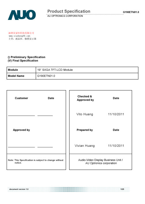
() Preliminary Specification(V) Final SpecificationModule 19” SXGA TFT-LCD Module Model Name G190ETN01.0Customer Date Approved byNote: This Specification is subject to change without notice.Checked &Approved by DateVito Huang11/10/2011 Prepared by Date Vivian Huang 11/10/2011Audio-Video Display Business Unit / AU Optronics corporation深圳市显恒科技有限公司www.xianheng99.com主营:液晶屏,触摸显示器Contents1. Handling Precautions (4)2. General Description (5)2.1 Display Characteristics (5)3. Functional Block Diagram (9)4. Absolute Maximum Ratings (10)4.1 TFT LCD Module (10)4.2 Absolute Ratings of Environment (10)5. Electrical characteristics (11)5.1 TFT LCD Module (11)6. Signal Characteristic (14)6.1 Pixel Format Image (14)6.2 The Input Data Format (14)6.3 Signal Description (15)6.4 Interface Timing (17)6.5 Power ON/OFF Sequence (19)7. Connector & Pin Assignment (20)7.1 TFT LCD Module (20)7.2 Backlight Unit (21)8. Reliability Test (22)9. Label and Packing (23)9.1. Shipping Label (23)9.2 Packing Form (23)9.3 Palletizing sequence (23)10. Outline Drawing (24)Record of RevisionVersion & Date Page Old Description New Description Remark 0.0 2011/09/13 All Frist Draft1.0 2011/11/10 23 Update Label and Packing1. Handling Precautions1) Since front polarizer is easily damaged, please be cautious and not to scratch it.2) Be sure to turn off power supply when inserting or disconnecting from input connector.3) Wipe off water drop immediately. Long contact with water may cause discoloration or spots.4) When the panel surface is soiled, wipe it with absorbent cotton or soft cloth.5) Since the panel is made of glass, it may be broken or cracked if dropped or bumped on hard surface.6) To avoid ESD (Electro Static Discharde) damage, be sure to ground yourself before handling TFT-LCD Module.7) Do not open nor modify the module assembly.8) Do not press the reflector sheet at the back of the module to any direction.9) In case if a module has to be put back into the packing container slot after it was taken out from the container, do not press the center of the LED light bar edge. Instead, press at the far endsof the LED light bar edge softly. Otherwise the TFT Module may be damaged.10) At the insertion or removal of the Signal Interface Connector, be sure not to rotate nor tilt the Interface Connector of the TFT Module.11) TFT-LCD Module is not allowed to be twisted & bent even force is added on module in a very short time. Please design your display product well to avoid external force applying to module by end-user directly.12) Small amount of materials without flammability grade are used in the TFT-LCD module. The TFT-LCD module should be supplied by power complied with requirements of Limited Power Source (IEC60950 or UL1950), or be applied exemption.13) Severe temperature condition may result in different luminance, response time and lamp ignition voltage.14) Continuous operating TFT-LCD display under low temperature environment may accelerate lamp exhaustion and reduce luminance dramatically.15) The data on this specification sheet is applicable when LCD module is placed in landscape position.16) Continuous displaying fixed pattern may induce image sticking. It’s recommended to use screen saver or shuffle content periodically if fixed pattern is displayed on the screen.2. General DescriptionG190ETN01.0 is a Color Active Matrix Liquid Crystal Display composed of a TFT-LCD panel, a driver circuit, and a backlight system. The screen format is intended to support the SXGA (1280(H) x 1024(V)) screen and 16.7M colors (RGB 6-bits + HiFRC data). All input signals are 2-channel LVDS interface.2.1 Display CharacteristicsThe following items are characteristics summary on the table under 25 condition:Items Unit SpecificationsScreen Diagonal [mm] 482.6 (19.0")Active Area [mm] 376.32 (H) x 301.06 (V)Pixels H x V 1280(x3) x 1024Pixel Pitch [mm] 0.294 (per one triad) x 0.294Pixel Arrangement R.G.B. Vertical StripeDisplay Mode Normally WhiteWhite Luminance [cd/m2] 350 (center, Typ) @60.0mAContrast Ratio 1000 : 1 (Typ)Optical ResponseTime [msec] 5 ms(Typ, on/off)Nominal Input Voltage VDD [Volt] +5.0 VPower Consumption [Watt] 14.5 W (Typ) (PDD= 4.7 W, PLED=9.8 W ) Weight [Grams] 1800 (Typ)Physical Size (H x V x D) [mm] 396 (H) x 324 (V) x 11.2(D) (Typ)Electrical Interface Dual channel LVDSSurface Treatment Hard-coating (3H), Non-Glare treatment Support Color 16.7M colors (RGB 6-bit + Hi_FRC)Temperature Range Operating Storage (Non-Operating) [o C][o C]0 to +50-20 to +60RoHS Compliance RoHS Compliance2.2 Optical CharacteristicsThe optical characteristics are measured under stable conditions at 25.ItemUnitConditionsMin. Typ. Max. NoteHorizontal (Right) CR = 10 (Left) 75 75 85 85 -Viewing Angle [degree] Vertical (Up) CR = 10 (Down) 70 70 80 80 - 2Contrast RatioNormal Direction 600 1000 - 3Raising Time (TrR)- 3.6 5.7 Falling Time (TrF) - 1.4 2.3 Optical Response Time[msec] Rising + Falling - 5 8 4 Red x 0.589 0.639 0.689 Red y 0.296 0.346 0.396 Green x0.274 0.324 0.374 Green y 0.577 0.6270.677 Blue x 0.104 0.154 0.204 Blue y 0.004 0.054 0.104 White x 0.263 0.313 0.363 Color / Chromaticity Coordinates (CIE)White y0.279 0.329 0.379 5 Central Luminance[cd/m 2 ] 280 350 - 6 Luminance Uniformity [%] 9 Points7580 -7 NTSC[%]72Optical Equipment: BM-5A, BM-7, PR880, or equivalentNote 1: Definition of viewing angleViewing angle is the measurement of contrast ratio≧10, or ≧5, at the screen center, over a 180° horizontal and 180° vertical range (off-normal viewing angles). The 180° viewing angle range is broken down as follows; 90° (θ) horizontal left and right and 90°(Φ) vertical, high (up) and low (down). The measurement direction is typically perpendicular to the display surface with the screen rotated about its center to develop the desired measurement viewing angle.Note 2: 9 points positionNote 3:Note 4: Measurement methodThe LCD module should be stabilized at given temperature for 30 minutes to avoid abrupt temperature change during measuring. In order to stabilize the luminance, the measurement should be executed after lighting Backlight for 30 minutes in a stable, windless and dark room.Note 5: Definition of response time:The output signals of photo detector are measured when the input signals are changed from “Full Black” to “Full White” (rising time), and from “Full White” to “Full Black” (falling time), respectively. The response time is intervalbetween the 10% and 90% of amplitudes. Please refer to the figure as below.3. Functional Block DiagramThe following diagram shows the functional block of the 19.0 inches wide Color TFT-LCD Module:4. Absolute Maximum RatingsAbsolute maximum ratings of the module are as following:4.1 TFT LCD Module4.2 Absolute Ratings of EnvironmentNote 1: With in Ta (25℃)Note 2: Permanent damage to the device may occur if exceeding maximum values Note 3: Temperature and relative humidity range are shown as the below figure.1. 90% RH Max ( Ta ≦39℃)2. Max wet-bulb temperature at 39℃ or less. ( Ta ≦39℃)3. No condensation Note 4: Function Judged onlyOperating Range Storage RangeItem SymbolMin Max Unit Conditions Logic/LCD DriveVoltageVDD-0.3+6.0[Volt]Note 1,2ItemSymbolMin.Max.UnitConditionsOperating Temperature TOP 0 +50 [o C] Note 3 Glass surface temperature (operation) TGS 0 +65 [o C] Note 3, Note 4Operation Humidity HOP 5 90 [%RH] Storage Temperature TST -20 +60 [o C] Storage HumidityHST590[%RH]Note 35. Electrical characteristics 5.1 TFT LCD Module5.1.1 Power SpecificationInput power specifications are as follows:Note 1: Measurement conditions:The duration of rising time of power input is 470us.Symbol ParameterMin Typ Max Unit ConditionsVDD Logic/LCD DriveVoltage 4.55.0 5.5[Volt] +/-10%IDD Input Current - 0.94 1.1 [A] VDD= 5.0V, All Black Pattern At 60Hz, PDDVDD Power - 4.7 5.5 [Watt] VDD= 5.0V, All Black Pattern At 60Hz IRush Inrush Current - - 3.0 [A]Note 1VDDrpAllowable Logic/LCD Drive Ripple Voltage--100[mV] p-p VDD= 5.0V, All Black Pattern At 75Hz5.1.2 Signal Electrical CharacteristicsInput signals shall be low or Hi-Z state when VDD is off. Please refer to specifications of SN75LVDS82DGG(Texas Instruments) in detail.Each signal characteristics are as follows; Symbol ParameterMin Typ Max Units ConditionV TH Differential Input High Threshold- - +100 [mV] V CM = 1.2V Note 1V TL Differential Input Low Threshold-100 - - [mV] V CM = 1.2V Note 1│V ID │ Input Differential Voltage 100 400 600 [mV] Note 1V TH -V TL = 200mV (max) V CMDifferential Input Common Mode Voltage+1.0+1.2+1.5[V]Note 1Note1: LVDS Signal Waveform5.1.3 Backlight unitParameter guideline for LED driving is under stable conditions at 25℃ (Room Temperature):Symbol Parameter Min. Typ. Max.Unit NoteIR LED LED Operation Current -60 -[mA] Note 1V LB Light Bar Operation Voltage(for reference) - 41 43.2 [Volt] Note 2 P BLU BLU Power consumption (for reference)- 9.8 - [Watt]LT LEDLED life Time (Typical)25,00030,000-[Hour] Note 3Operating with fixed driving currentNote 1 :The specified current is input LED chip 100% duty current.Note 2 : The value showed in the table is one light bar’s operation voltage.Note 3 : Definition of life time : brightness becomes 50% of its original value. The minimum life time of LED unit is on thecondition of IR LED = 60mA and 25±2℃(Room temperature).Note 4: Each LED light bar consists of 48 pcs LED package ( 4 strings x 12 pcs / string ).6. Signal Characteristic 6.1 Pixel Format ImageFollowing figure shows the relationship of the input signals and LCD pixel format.121279 1280 1st Line1024th LineNote1: Normally, DE, VS, HS on EVEN channel are not used. Note2: Please follow PSWG. Note3: 8-bit in6.3 Signal DescriptionThe module using one LVDS receiver SN75LVDS82(Texas Instruments). LVDS is a differential signal technology for LCD interface and high speed data transfer device. LVDS transmitters shall beSN75LVDS83(negative edge sampling). The first LVDS port(RxOxxx) transmits odd pixels while the second LVDS port(RxExxx) transmits even pixels.PIN # SIGNAL NAME DESCRIPTION1 RxOIN0-Negative LVDS differential data input (Odd data)2 RxOIN0+Positive LVDS differential data input (Odd data)3 RxOIN1-Negative LVDS differential data input (Odd data)4 RxOIN1+Positive LVDS differential data input (Odd data)5 RxOIN2-Negative LVDS differential data input (Odd data, DSPTMG)6 RxOIN2+Positive LVDS differential data input (Odd data, DSPTMG)7 GND Power Ground8 RxOCLKIN-Negative LVDS differential clock input (Odd clock)9 RxOCLKIN+Positive LVDS differential clock input (Odd clock)10 RxOIN3-Negative LVDS differential data input (Odd data)11 RxOIN3+Positive LVDS differential data input (Odd data)12 RxEIN0-Negative LVDS differential data input (Even data)13 RxEIN0+Positive LVDS differential data input (Even data)14 GND Power Ground15 RxEIN1-Positive LVDS differential data input (Even data)16 RxEIN1+Negative LVDS differential data input (Even data)17 GND Power Ground18 RxEIN2-Negative LVDS differential data input (Even data)19 RxEIN2+Positive LVDS differential data input (Even data)20 RxECLKIN-Negative LVDS differential clock input (Even clock)21 RxECLKIN+Positive LVDS differential clock input (Even clock)22 RxEIN3-Negative LVDS differential data input (Even data)23 RxEIN3+Positive LVDS differential data input (Even data)24 GND Power Ground25 GND Power Ground26 NC No connection (for AUO test)27 NC No connection (for AUO test)28 POWER Power +5V29 POWER Power +5V30 POWER Power +5VNote1: Start from left sideNote2: Input signals of odd and even clock shall be the same timing.6.4 Interface Timing6.4.1 Timing CharacteristicsSignal ItemSymbol MinTypMaxUnit Period Tv 103210661150Th ActiveTdisp(v) 1024 1024 1024 Th Vertical Section Blanking Tbp(v)+Tfp(v)+PWvs842126ThPeriod Th780 844 2047 Tclk Active Tdisp(h) 640 640640 TclkHorizontal Section Blanking Tbp(h)+Tfp(h)+PWhs140 204 -Tclk PeriodTclk22.2 18.52 14.81 nsClockFrequency Freq. 45 54 67.5 MHz Frame RateFrequency1/Tv506075HzNote: DE mode onlyAU OPTRONICS CORPORATIONProduct SpecificationG190ETN01.06.4.2 Timing DiagramHsyncPixel N1M Invalid DataTdisp(v)10DEDEInvalid Data RGB DataTh2RGB Data (Even)39M-1Invalid Data1N HsyncM-2Invalid Data1165M-3Vsync Invalid DataCLKM-5Invalid DataM-472Tbp(h)Pixel Pixel Pixel Pixel Pixel RGB Data(Odd)12Tbp(v)Tclk Pixel Pixel Pixel Pixel Pixel Pixel Pixel PixelPixelPixel Pixel Pixel 8434TvTdisp(h)LineLineLineLineLineLineTfp(v)Tfp(h)PWvsPWhs6.5 Power ON/OFF SequenceVDD power and lamp on/off sequence are as follows. Interface signals are also shown in the chart. Signals from any system shall be Hi-Z state or low level when VDD is off.Note1: insert a white pattern 360ms Note2: insert a black patternNote3 :insert a white pattern after valid data and last until VDD falls to 10%. Note4 :when AC on/off, timing rule of logo power on/off is the same as above.Power Sequence Timing ValueParameterMin. Typ. Max. UnitsT1 0.5 - 10T2 040 50 T3 500 -- T4 300 -- T5 40 1500 - T6 -- -T71000 --msLVDS SignalBacklight OnPower Supply VDD7. Connector & Pin AssignmentPhysical interface is described as for the connector on module.These connectors are capable of accommodating the following signals and will be following components.7.1 TFT LCD Module7.1.1 ConnectorConnector Name / Designation Interface Connector / Interface card Manufacturer P-TWO / JAEType Part Number 187034-30091 / FI-XB30SSLA-HF15Mating Housing Part Number FI-X30HLFI-X30H (Unlocked Type)7.1.2 Pin AssignmentPin#Signal Name Pin#Signal Name1 RxOIN0-2 RxOIN0+3 RxOIN1-4 RxOIN1+5 RxOIN2-6 RxOIN2+7 GND 8 RxOCLKIN-9 RxOCLKIN+ 10 RxOIN3-11 RxOIN3+ 12 RxEIN0-13 RxEIN0+ 14 GND15 RxEIN1- 16 RxEIN1+17 GND 18 RxEIN2-19 RxEIN2+ 20 RxECLKIN-21 RxECLKIN+ 22 RxEIN3-23 RxEIN3+ 24 GND25 GND 26 NC27 NC 28 POWER29 POWER 30 POWER7.2 Backlight UnitPhysical interface is described as for the connector on module. These connectors are capable of accommodating the following signals and will be following components.7.2.1 ConnectorConnector Name / Designation Light Bar ConnectorManufacturer ENTERY INDUSTRIAL CO., LTDType Part Number 3707K-S06N-01R7.2.2 Pin AssignmentPin no. Signal name1 IRLED (current out)2 IRLED (current out)3 VLED (voltage in)4 VLED (voltage in)5 IRLED (current out)6 IRLED (current out)8. Reliability TestEnvironment test conditions are listed as following table.Items Required Condition Note Temperature Humidity Bias (THB) Ta= 580%RH, 300hoursHigh Temperature Operation (HTO) Ta= 550%RH, 300hoursLow Temperature Operation (LTO) Ta=High Temperature Storage (HTS) Ta=Low Temperature Storage (LTS) Ta= -Vibration Test (Non-operation) Acceleration: 1.5 GWave: Random Frequency: 10 - 200 - 10 Hz Sweep: 30 Minutes each Axis (X, Y, Z)Shock Test (Non-operation) Acceleration: 50 GWave: Half-sineActive Time: 20 msDirection: ±X,±Y,±Z (one time for each Axis)Drop Test Height: 60 cm, package testThermal Shock Test (TST) -30min, 630min, 100 cyclesOn/Off Test On/10sec, Off/10sec, 30,000 cyclesContact Discharge: ± 8KV, 150pF(330Ω ) 1sec,9 points, 25 times/ point.ESD (Electro Static Discharge)Air Discharge: ± 15KV, 150pF(330Ω ) 1sec9 points, 25 times/ point.1Altitude Test Operation:10,000 ftNon-Operation:30,000 ftNote1: According to EN61000-4-2, ESD class B: Some performance degradation allowed. No data lost Self-recoverable. No hardware failures.Note2:Water condensation is not allowed for each test items.Each test is done by new TFT-LCD module. Don’t use the same TFT-LCD module repeatedly for reliability test.The reliability test is performed only to examine the TFT-LCD module capability.To inspect TFT-LCD module after reliability test, please store it at room temperature and room humidity for 24 hours at least in advance.No function failure occurs.9. Label and Packing9.1. Shipping Label9.2 Packing FormMax. capacity: 13 pieces TFT-LCD module per cartonMax. weight: 26.69 kg per cartonOutside dimension of carton: 409(L)mm* 367(W)mm* 475(H)mmPallet : 1140(L)mm*830 (W)mm* 1560(H)mm9.3 Palletizing sequencepcs / box box / layer layer / pallet pcs / pallet Shipping by air 13 6 3 234 Shipping by sea 13 6 3 234A U O P T R O N I C S C O R P O R A T I O NP r o d u c t S p e c i f i c a t i o nd o c u me n t v e r s i o n 1.0 24/25G 190E T N 01.0A U O P T R O N I C S C O R P O R A T I O NP r o d u c t S p e c i f i c a t i o nd o c u me n t v e r s i o n 1.0 25/25G 190E T N 01.0。
友达10.4寸G104STN01.0液晶屏规格书-杭州旭虹科技

( V ) Preliminary Specifications( ) Final SpecificationsModule 10.4 Inch Color TFT-LCD Model Name G104STN01.0Customer Date Checked &Approved by Approved by DateGrace Hung 2013/08/16 Prepared byJohnson Lin 2013/08/16 General Display Business Division / AU Optronics corporationContents1. Operating Precautions (4)2. General Description (5)2.1 Display Characteristics (5)2.2 Optical Characteristics (6)3. Functional Block Diagram (9)4. Absolute Maximum Ratings (10)4.1 Absolute Ratings of TFT LCD Module (10)4.2 Absolute Ratings of Environment (10)5. Electrical Characteristics (11)5.1 TFT LCD Module (11)5.2 Backlight Unit (13)6. Signal Characteristics (14)6.1 Pixel Format Image (14)6.2 Scanning Direction (14)6.3 TFT-LCD Interface Signal Description (15)6.4 The Input Data Format (16)6.5 TFT-LCD Interface Timing (17)6.6 Power ON/OFF Sequence (18)7. Connector & Pin Assignment (19)7.1 TFT-LCD Signal (CN1): LVDS Connector (19)7.2 LED Backlight Unit (CN2): Driver Connector (19)7.3 LED Backlight Unit (CN4): Light bar Connector (19)8. Reliability Test Criteria (20)9. Mechanical Characteristics (21)9.1 LCM Outline Dimension (Front View) (21)9.2 LCM Outline Dimension (Rear View) (22)10. Label and Packaging (23)10.1 Shipping Label (on the rear side of TFT-LCD display) (23)10.2 Carton Package (23)11 Safety (25)11.1 Sharp Edge Requirements (25)11.2 Materials (25)11.3 Capacitors (25)11.4 National Test Lab Requirement (25)Record of RevisionVersion and Date Page Old description New Description1. Operating Precautions1) Since front polarizer is easily damaged, please be cautious and not to scratch it.2) Be sure to turn off power supply when inserting or disconnecting from input connector.3) Wipe off water drop immediately. Long contact with water may cause discoloration orspots.4) When the panel surface is soiled, wipe it with absorbent cotton or soft cloth.5) Since the panel is made of glass, it may be broken or cracked if dropped or bumped onhard surface.6) To avoid ESD (Electro Static Discharde) damage, be sure to ground yourself before handlingTFT-LCD Module.7) Do not open nor modify the module assembly.8) Do not press the reflector sheet at the back of the module to any direction.9) In case if a module has to be put back into the packing container slot after it was takenout from the container, do not press the center of the LED light bar edge. Instead, press at the far ends of the LED light bar edge softly. Otherwise the TFT Module may be damaged.10) At the insertion or removal of the Signal Interface Connector, be sure not to rotate nortilt the Interface Connector of the TFT Module.11) TFT-LCD Module is not allowed to be twisted & bent even force is added on module in a veryshort time. Please design your display product well to avoid external force applying to module by end-user directly.12) Small amount of materials without flammability grade are used in the TFT-LCD module. TheTFT-LCD module should be supplied by power complied with requirements of Limited Power Source (IEC60950 or UL1950), or be applied exemption.13) Severe temperature condition may result in different luminance, response time and lampignition voltage.14) Continuous operating TFT-LCD display under low temperature environment may acceleratelamp exhaustion and reduce luminance dramatically.15) The data on this specification sheet is applicable when LCD module is placed in landscapeposition.16) Continuous displaying fixed pattern may induce image sticking. It’s recommended to usescreen saver or shuffle content periodically if fixed pattern is displayed on the screen.2. General DescriptionThis specification applies to the Color Active Matrix Liquid Crystal Display G104STN01.0composed of a TFT-LCD display, a driver and power supply circuit, and a LED backlight system. The screen format is intended to support SVGA (800(H) x 600(V)) screen and 16.2M (RGB 8-bits) or 262k colors (RGB 6-bits).LED driving board for backlight unit is included in G104STN01.0 and the LED unit is replaceable. All input signals are LVDS interface and compatible with G104SN02 V2.G104STN01.0 designed with wide viewing angle; wide temperature and long life LED backlight is well suited for industial applications. G104STN01.0 is a RoHS product.2.1 Display CharacteristicsThe following items are characteristics summary on the table under 25 ℃ condition: ItemsUnitSpecifications Screen Diagonal [inch] 10.4Active Area [mm] 211.2 (H) x 158.4 (V) Pixels H x V 800 x 3(RGB) x 600 Pixel Pitch [mm] 0.264 x 0.264 Pixel Arrangement R.G.B. Vertical Stripe Display ModeTN, Normally White Nominal Input Voltage VDD [Volt] 3.3 (typ.) Typical Power Consumption [Watt] 2.88WAll black pattern Weight [Grams] 365(Typ.)Physical Size [mm] 243.0(H) x 184.0(V) x 6.5(D)(Typ.) Electrical Interface 1 channel LVDS Surface Treatment Anti-glare, Hardness 3H Support Color16.2M / 262K colors Temperature Range OperatingStorage (Non-Operating) [o C] [o C]-20 to +80 -20 to +80 RoHS ComplianceRoHS Compliance2.2 Optical CharacteristicsThe optical characteristics are measured under stable conditions at 25 (Room Temperature):℃Item Unit Conditions Min. Typ. Max. RemarkWhite Luminance[cd/m2] I F = 50mA/1 LED Line (center point) 300 400 -1 Uniformity % 5 Points 65 75 -2,3 Contrast Ratio500 700 - 4[msec]Rising - 10 20 [msec] Falling- 5 15 Response Time[msec] Raising + Falling - 15 35 5 [degree] [degree] Horizontal (Right) CR = 10 (Left) 70 70 80 80 - - Viewing Angle[degree] [degree]Vertical (Upper) CR = 10 (Lower) 50 60 60 70 - - 6 Red x - TBD - Red y - TBD - Green x- TBD - Green y - TBD - Blue x - TBD - Blue y - TBD - White x 0.28 0.31 0.34 Color / ChromaticityCoordinates (CIE 1931)White y0.30 0.33 0.36 Color Gamut%50-Note 1: Measurement method Equipment Pattern Generator, Power Supply, Digital Voltmeter, Luminance meter (SR_3 or equivalent) Aperture1with 50cm viewing distance ∘Test Point CenterEnvironment < 1 luxModule Driving EquipmentNote 2: Definition of 5 points position (Display active area: 211.2mm (H) x 158.4mm (V))Note 3: The luminance uniformity of 5 points is defined by dividing the minimum luminance values by the maximum test point luminanceNote 4: Definition of contrast ratio (CR):Note 5: Definition of response time:The output signals of photo detector are measured when the input signals are changed from “White” to “Black” (falling time) and from “Black” to “White” (rising time), respectively. The response time interval isNote 6: Definition of viewing angleViewing angle is the measurement of contrast ratio 10, at the screen center, over a 180° horizontal and ≧180° vertical range (off-normal viewing angles). The 180° viewing angle range is broken down as below: 90° (θ) horizontal left and right, and 90° (Φ) vertical high (up) and low (down). The measurement direction is typically perpendicular to the display surface with the screen rotated to its center to develop the desiredMinimum Brightness of five pointsδW9 = Maximum Brightness of five points Contrast ratio (CR)=Brightness on the “White” stateBrightness on the “Black” statemeasurement viewing angle.3. Functional Block DiagramThe following diagram shows the functional block of the 10.4 inch color TFT/LCD module:4. Absolute Maximum Ratings4.1 Absolute Ratings of TFT LCD ModuleItem Symbol Min Max Unit Logic/LCD Drive Voltage Vin -0.3 +4.0 [Volt]4.2 Absolute Ratings of EnvironmentItem Symbol Min Max Unit Operating Temperature TOP -20 +80 [o C] Operation Humidity HOP 5 95 [%RH] Storage Temperature TST -20 +80 [o C] Storage Humidity HST 5 95 [%RH] Note: Maximum Wet-Bulb should be 39℃ and no condensation.5. Electrical Characteristics 5.1 TFT LCD Module5.1.1 Power SpecificationSymbol Parameter Min Typ Max Units RemarkVDD Logic/LCD Input Voltage 3.0 3.3 3.6 [Volt]I VDD LCD Input Current - 320 - [mA]VDD=3.3V at 60 HZ, all Black PatternP VDD LCD Power comsumption - - 1.5 [Watt] VDD=3.3V at 60 HZ, all Black Pattern I rush LCDLCD Inrush Current-1.06-[A] Note 1; VDD=3.3VBlack Pattern, Rising time=470usVDD rpAllowable Logic/LCDDrive Ripple Voltage- -100 [mV] p-pVDD=3.3V at 60 HZ, all Black PatternNote 1: Measurement condition:VDD rising time0V3.3V5.1.2 Signal Electrical CharacteristicsInput signals shall be low or Hi-Z state when VDD is off.Note: LVDS Signal Waveform.Symbol ItemMin. Typ.Max. Unit RemarkVTH Differential Input High Threshold - - 100 [mV] VCM=1.2V VTL Differential Input Low Threshold 100 - - [mV] VCM=1.2V |VID |Input Differential Voltage100 400 600 [mV] VICMDifferential Input Common Mode Voltage1.1251.251.375[V]VTH/VTL=+-100mV5.2 Backlight Unit5.2.1 Parameter guideline for LED backlightFollowing characteristics are measured under a stable condition using a inverter at 25℃. (Room Temperature): Symbol Parameter Min.Typ.Max.Unit RemarkVCC Input Voltage 10.8 12 12.6 [Volt]I VCC Input Current - 0.32 - [A] 100% PWM DutyP VCC Power Consumption - 2.88 - [Watt] 100% PWM DutyF PWM Dimming Frequency 200 - 20K [Hz]Swing Voltage 3 3.3 5.5 [Volt]Dimming duty cycle 5 - 100 %I F LED Forward Current-50 -[mA] Ta = 25o C- 27.2 - [Volt]I F = 50mA, Ta = -30o C V F LED Forward Voltage- 26.4 28.8 [Volt]I F = 50mA, Ta = 25o C- 25.6 - [Volt]I F = 50mA, Ta = 85o C P LED LED Power Consumption- 2.72 - [Watt]Operation Life 50,000 - - Hrs I F=50mA, Ta= 25o CNote 1: Ta means ambient temperature of TFT-LCD module.Note 2: VCC, I VCC, I rush LED, P VCC are defined for LED backlight.(100% duty of PWM dimming)Note 3: I F, V F are defined for one channel LED. There are two LED channel in back light unit.Note 4: If G104STN01.0 module is driven by high current or at high ambient temperature & humidity condition. The operating life will be reduced.Note 5: Operating life means brightness goes down to 50% initial brightness. Minimum operating life time is estimated data.6. Signal Characteristics6.1 Pixel Format ImageFollowing figure shows the relationship between input signal and LCD pixel format.1st2nd799th800th1stLine600thLin6.2 Scanning DirectionThe following figures show the image seen from the front view. The arrow indicates the direction of scan.Fig. 1 Normal scan (Pin4, DPS = Low or NC) Fig. 2 Reverse scan (Pin4, DPS = High)6.3 TFT-LCD Interface Signal DescriptionThe module using a LVDS receiver embaded in AUO’s ASIC. LVDS is a differential signal technology for LCD interface and a high-speed data transfer device.Input Signal Interface Pin No. SymbolDescription 1 VDD Power Supply, 3.3V (typical) 2 VDD Power Supply, 3.3V (typical) 3 GND Ground4 DPS Reverse Scan Function [H: Enable; L/NC: Disable]5 RxIN0-6 RxIN0+ LVDS receiver signal channel 0LVDS Differential Data Input (R0, R1, R2, R3, R4, R5, G0)7 GND Ground8 RxIN1- 9 RxIN1+ LVDS receiver signal channel 1LVDS Differential Data Input (G1, G2, G3, G4, G5, B0, B1) 10 GND Ground11 RxIN2- 12 RxIN2+ LVDS receiver signal channel 2LVDS Differential Data Input (B2, B3, B4, B5, DE)13 GNDGround14 RxCLKIN- 15 RxCLKIN+ LVDS receiver signal clock 16 GND Ground17 RxIN3- 18 RxIN3+ LVDS receiver signal channel 3, pin17=3.3V&pin 18=GND for 6bit LVDS InputLVDS Differential Data Input (R6, R7, G6, G7, B6, B7, RSV)19 RSVReserved for AUO internal test. Please treat it as NC.20SEL68 6/8bits LVDS data input selection [H: 8bits L/NC: 6bit]Note 1: Input Signals shall be in low status when VDD is off.Note 2: High stands for “3.3V”, Low stands for “0V”, NC stands for “No Connection”. Note 3: RSV stands for “Reserved”.6.4 The Input Data Format6.4.1 SEL68SEL68 =“Low” or “NC” for 6 bits LVDS InputSEL68 = “High” for 8 bits LVDS InputNote1: Please follow PSWG.Note2: R/G/B data 7:MSB, R/G/B data 0:LSBSignal Name DescriptionRemarkR7R6R5R4R3R2R1R0Red Data 7 Red Data 6 Red Data 5 Red Data 4 Red Data 3 Red Data 2 Red Data 1 Red Data 0 Red-pixel DataFor 8Bits LVDS input MSB: R7 ; LSB: R0For 6Bits LVDS input MSB: R5 ; LSB: R0G7G6G5G4 G3G2G1 G0Green Data 7 Green Data 6 Green Data 5 Green Data 4Green Data 3 Green Data 2 Green Data 1Green Data 0 Green-pixel DataFor 8Bits LVDS input MSB: G7 ; LSB: G0For 6Bits LVDS input MSB: G5 ; LSB: G0B7 B6 B5 B4 B3 B2 B1 B0 Blue Data 7 Blue Data 6 Blue Data 5 Blue Data 4 Blue Data 3 Blue Data 2 Blue Data 1 Blue Data 0 Blue-pixel DataFor 8Bits LVDS input MSB: B7 ; LSB: B0For 6Bits LVDS input MSB: B5 ; LSB: B0 RxCLKIN LVDS Data ClockDE Data Enable SignalWhen the signal is high, the pixel data shall be valid to be displayed.Note: Output signals from any system shall be low or Hi-Z state when VDD is off.NS-like format6.5 TFT-LCD Interface Timing6.5.1 Timing CharacteristicsSignal Symbol Min. Typ. Max. Unit Clock Frequency 1/ T Clock 30 40 50 MHzPeriod T V 608 628 1024 Active T VD -- 600-- Vertical SectionBlankingT VB 8 28 424 T Line Period T H 960 1056 1060Active T HD -- 800 -- Horizontal SectionBlankingT HB 160 256 260 T ClockFrame RateF 506075Hz Note : DE mode.6.5.2 Input Timing DiagramDOTCLKDEHT HBDET VDInput Timing Definition ( DE Mode)Input Data Invaild Data Invaild Data6.6 Power ON/OFF SequenceVDD power and lamp on/off sequence is as below. Interface signals are also shown in the chart. Signals from any system shall be Hi-Z state or low level when VDD is off.Power ON/OFF sequence timingValue UnitsParameterMin. Typ. Max.T10.5 - 10 [ms]T2 30 40 50 [ms]T3 200 -- -- [ms]T4 0.5 -- 10 [ms]T5 10 - - [ms]T6 10 - - [ms]T7 0 - - [ms]T8 10 - - [ms]T9 -- -- 10 [ms]T10 110 -- -- [ms]T11 0 16 50 [ms]T12 - - 10 [ms]T13 1000 - - [ms]The above on/off sequence should be applied to avoid abnormal function in the display. Please make sure to turn off the power when you plug the cable into the input connector or pull the cable out of the connector.7. Connector & Pin AssignmentPhysical interface is described as for the connector on module. These connectors are capable of accommodating the following signals and will be following components.7.1 TFT-LCD Signal (CN1): LVDS ConnectorConnector Name / Designation Signal ConnectorManufacturer STM or compatibleConnector Model Number MSB24013P20HA or compatibleAdaptable Plug P24013P20 or compatiblePin No. Symbol Pin No. Symbol1 VDD2 VDD3 GND4 DPS5 RxIN0-6 RxIN0+7 GND 8 RxIN1-9 RxIN1+ 10 GND11 RxIN2- 12 RxIN2+13 GND 14 RxCKIN-15 RxCKIN+ 16 GND17 RxIN3- 18 RxIN3+19 RSV 20 SEL687.2 LED Backlight Unit (CN2): Driver ConnectorConnector Name / Designation Lamp ConnectorManufacturer ENTERY or compatibleConnector Model Number 3808K-F05N-12R or compatibleMating Model Number H208K–P05N-02B or compatiblePin No. symbol descriptionPin1 VCC 12V inputPin2 GND GNDPin3 On/OFF 5V-ON,0V-OFFPin4 Dimming PWMPin5 NA7.3 LED Backlight Unit (CN4): Light bar ConnectorConnector Name / Designation Lamp ConnectorManufacturer ENTERY or compatibleConnector Model Number H208K–P03N-02B or compatibleMating Model Number(CN3) 3808K-F03N-12R or compatiblePin No. symbol description ColorPin1 H LED anode RedPin2 L LED cathode WhitePin3 L LED cathode Black8. Reliability Test CriteriaItems Required Condition Note Temperature Humidity Bias 40℃, 90%RH, 300 hoursHigh Temperature Operation 80℃, 300 hoursLow Temperature Operation -20℃, 300 hoursHot Storage 80,℃ 300 hoursCold Storage -20,℃ 300 hoursThermal Shock Test -20/℃ 30 min, 60/℃ 30 min, 100cycles, 40℃minimun ramp rateHot Start Test 80℃/ 1Hr min. power on/off per 5 minutes, 5 timesCold Start Test -20℃/ 1Hr min. power on/off per 5 minutes, 5 timesShock Test (Non-Operating) 50G, 20ms, Half-sine wave, ( ±X, ±Y, ±Z)Vibration Test (Non-Operating) 1.5G, (10~200Hz, Sine wave)30 mins/axis, 3 direction (X, Y, Z)On/off test On/10 sec, Off/10 sec, 30,000 cyclesESD Contact Discharge: ± 8KV, 150pF(330Ω ) 1sec, 8 points, 25 times/ pointAir Discharge: ± 15KV, 150pF(330Ω ) 1sec, 8 points, 25 times/ pointNote 1EMI 30-230 MHz, limit 40 dBu V/m, 230-1000 MHz, limit 47 dBu V/mNote1: According to EN61000-4-2, ESD class B: Some performance degradation allowed. No data lost Self-recoverable. No hardware failures.Note2:Water condensation is not allowed for each test items.Each test is done by new TFT-LCD module. Don’t use the same TFT-LCD module repeatedly for reliability test. The reliability test is performed only to examine the TFT-LCD module capability.To inspect TFT-LCD module after reliability test, please store it at room temperature and room humidity for 24 hours at least in advance.G104STN01.09. Mechanical Characteristics工业液晶屏:www.hzxuhong.com杭州旭虹科技有限公司G104STN01.09.2 LCM Outline Dimension (Rear View)工业液晶屏:www.hzxuhong.com杭州旭虹科技有限公司G104STN01.010. Label and Packaging10.1 Shipping Label (on the rear side of TFT-LCD display)10.2 Carton PackageNote:Max capacity :20 TFT-LCD module per cartonMax weight: 11.5 kg per cartonOutside dimension of carton: 477mm(L)* 290mm(W)*360mm(H)Pallet size : 1180 mm * 980 mm * 135mmBox stackedModule by air :(2 *4) *4 layers ,one pallet put 32 boxes ,total 640pcs module Module by sea :(2 *4) *4 layers + (2 *4) *1 layers , two pallet put 40 boxes ,total 800pcs module Module by sea_HQ :(2 *4) *4 layers+(2 *4) *2 layers, two pallet put 48 boxes, total 960pcs module工业液晶屏:www.hzxuhong.com杭州旭虹科技有限公司杭州旭虹科技有限公司11 Safety11.1 Sharp Edge RequirementsThere will be no sharp edges or comers on the display assembly that could cause injury.11.2 Materials11.2.1 ToxicityThere will be no carcinogenic materials used anywhere in the display module. If toxic materials are used, they will be reviewed and approved by the responsible AUO toxicologist.11.2.2 FlammabilityAll components including electrical components that do not meet the flammability grade UL94-V1 in the module will complete the flammability rating exception approval process.The printed circuit board will be made from material rated 94-V1 or better. The actual UL flammability rating will be printed on the printed circuit board.11.3 CapacitorsIf any polarized capacitors are used in the display assembly, provisions will be made to keep them from being inserted backwards.11.4 National Test Lab RequirementThe display module will satisfy all requirements for compliance to:UL 1950, First EditionU.S.A. Information Technology Equipment杭州旭虹科技有限公司。
G190ETN01.2友达19寸宽温工控液晶屏-杭州旭虹科技有限公司

22
Update 9. Label and Packing
24
Update 10. Outline Drawing
document version 1.0
3/25
Product Specification
AU OPTRONICS CORPORATION
G190ETN01.2
1. Handling Precautions
Product Specification
AU OPTRONICS CORPORATION
G190ETN01.2
() Preliminary Specification (V) Final Specification
Module Model Name
19” SXGA TFT-LCD Module G190ETN01.2
New Description
1.0 2014/04/07 5
Update Power Consumption and Weight
6ห้องสมุดไป่ตู้
Update 2.2 Optical Characteristics
10
Update 4.2 Absolute Ratings of Environment
13
Update 5.1.3 Backlight Unit
Customer
Date
Checked & Approved by
Vito Huang
Date
2014/04/07
Approved by
Prepared by
Date
Vivian Huang
2014/04/04
Note: This Specification is subject to change without notice.
三菱TFT液晶屏型号
※1 PCAP: 投射型电容方式 ※2 ITO: 铟锡氧化物 ※3:除了3.5寸-5.7寸的产品 ※4:同时触摸2点或2点以上进行的操作
多点触控操作
防护玻璃 传感器电路板 LCD液晶模块
触摸屏的简单示意图
检测布线
耐噪声
灵敏度
搭载四线电阻式触摸屏的液晶模块
我们可提供高通用性、对应各种工业设备领域需求的四线 电阻式触摸屏与工业用液晶模块相结合的产品阵容。借助 液晶模块与触摸屏产品组装的一条龙生产实现高可靠性。
以往形式
保护玻璃 空气层 LCD
玻璃粘结型形式
保护玻璃 接合树脂 LCD
由于反射显示效果不佳
反射极少(1/10以下的反射率)
半透半反射型TFT液晶模块
半透半反射型液晶模块兼具透射和反射模式,可 分别利用背光或环境光作为光源。透射模式可在 昏暗环境下提供高可视性,反射模式可在强光环 境下无需利用背光亮度来维持高可视性。因此,半 透半反射型TFT液晶模块可大大节约功耗,可谓 是工业便携设备的最佳选择。三菱电机已经开始 批量生产5.7寸、8.4寸模块,今后还将进一步扩 充产品线。
AA084XD01ADA11 NEW
AA084XD11
XGA
AA084XD11ADA11 NEW
(1024x768) AA084XE01
AA084XE01ADA11 NEW
AA084XE11
AA084XE11ADA11 NEW
AA090ME01
Wide-VGA AA090ME01--T1
(800x480) AA090MH01
三菱电机工业用彩色TFT液晶模块 杭州旭虹科技有限公司
工业液晶屏www.hzxuhong.com
MTFoTdLuCleDs
天马3.5寸工业液晶屏TM035KDH03规格书-杭州旭虹科技有限公司
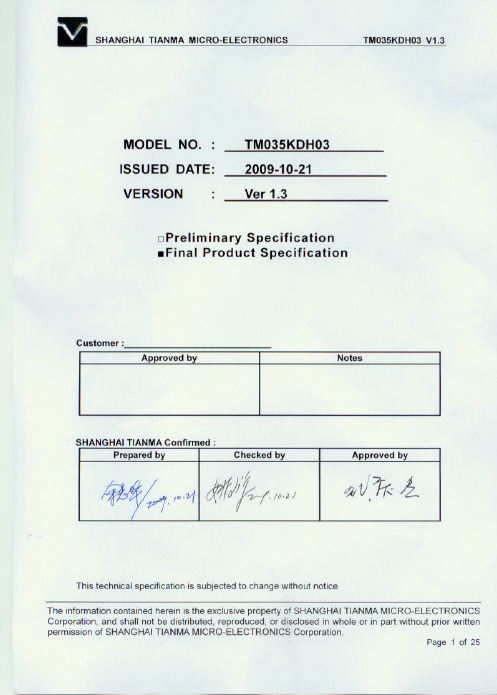
杭州旭虹科技有限公司
SHANGHAI TIANMA MICRO-ELECTRONICS TM035KDH03 V1.3
Table of Contents
Coversheet........................................................................................................................................ 1 Record of Revision............................................................................................................................ 3 1. 2. 3 4 5 6 7 8 9 General Specifications ............................................................................................................... 4 Input/Output Terminals ............................................................................................................... 5 Absolute Maximum Ratings ....................................................................................................... 8 Electrical Characteristics............................................................................................................ 8 Timing Chart............................................................................................................................. 10 Optical Characteristics ............................................................................................................. 17 Environmental / Reliability Tests............................................................................................... 21 Mechanical Drawing................................................................................................................. 22 Packing drawing ...................................................................................................................... 23
XH70745B7寸电容触摸屏规格书-杭州旭虹科技有限公司)
边沿区域漏光宽度≤0.25mm
★
边沿区域漏光宽度>0.25mm
★
ITO表面不允许有不可清洁处理的脏
污、水印
★
无法清洁的脏污按点状不良判定
★
FPC 缺陷
凹痕,针孔 a≤w/3
★
开路/划伤线路/裂开
★
氧化,污染
★
FPC 折伤
FPC 折伤/压伤 ;死折(锐角折痕)不
允许,锐角凸起
★
6. Notice 注意事项
NO PART OF THIS SPECIFICATION MAY BE REPRODUCED OR TRANSMITTED IN ANY FORM OR BY ANY MEANS WITHOUT THE EXPRESSED WRITTEN PERMISSION OF WGJ.
工业液晶屏http://www.hzxuhong.com
80ºC,240hrs -30ºC,240hrs 60ºC/90% RH,240hrs
70ºC,24hrs -20 ºC,24hrs 60ºC/90%RH,24hrs -30 ~ 80℃, 60 Mins/cycle , Total 10
Cycles
4. Touch panel description 触摸屏功能描述
Date 日期 Ver.版
Hangzhou Xu Hong Technology Co.,Ltd
History of Version 变更记录
Description 描述
Page 页 Design by 变更人
2016-02-27
A0 在 XH70745A-GDA-A1 基础上更改盖板
10/10
LLL
2016-03-15
友达B140XW01 V8 PDF

LED Backlight with driving circuit design
Customer
Date
Checked & Approved by
Date
Approved by
www.DataSheet.co.kr
Bonnie Chen
Date
10/28/2009
7. Panel Reliability Test ............................................................ 22
7.1 Vibration Test ....................................................................................................................................22 7.2 Shock Test .....................................................www..DataS.heet.c.o.kr.................................................................................22 7.3 Reliability Test...................................................................................................................................22
3 of 30
友达8.4寸G084SN05 v7规格书-杭州旭虹科技有限公司

工业液晶屏www.hzxuhong.com
(V ) Preliminary Specifications ( ) Final Specifications Module Model Name 8.4 Inch Color TFT-LCD G084SN05 V7
Customer
Date
Approvehiu
2008/1/14
Checked & Approved by
Prepared by
ALEX Cheng
2008/1/14
Note: This Specification is subject to change without notice.
General Display Business Division / AU Optronics corporation
4.1 Absolute Ratings of TFT LCD Module.............................................................................. 10 4.2 Absolute Ratings of Environment..................................................................................... 10
Viewing Angle 70/70/65/55(R/L/U/D)
Lamp Life Typ. 50,000hrs
Viewing Angle 75/75/75/75(R/L/U/D)
Lamp Life Min. 50,000hrs VCFL:430 v PCFL:5.16 w 7.1.1 Connector Illustration
vl-ps-cog-vlbot005-01 10.4寸车载rev.a杭州旭虹科技

Figure 1. Function Diagram 1.2 Features0.5t Glass (Single)Figure 2. The TFT and CF Align Direction 3. LCM weight tolerance: ± 5%友达奇美群创天马液晶屏代理商-杭州旭虹科技工业液晶屏:www.hzxuhong.comVL-PS-COG-VLBOT005-01 REV. A (COG-VLBOT005-01) AUG/2016 PAGE 11 OF 235.3 LVDS Input Signal Format6bit MODE8bit MODE Figure 4. LVDS Input Signal Format工业液晶屏:www.hzxuhong.com友达奇美群创天马液晶屏代理商-杭州旭虹科技工业液晶屏:www.hzxuhong.comVL-PS-COG-VLBOT005-01 REV. A (COG-VLBOT005-01) AUG/2016 PAGE 12 OF 236.0 OPTICAL SPECIFICATION 6.1 OverviewThe test of Optical specifications shall be measured in a dark room(ambient luminance≤ 1 lux and temperature = 25±2℃) with the equipment of Luminance meter system (Topcon SR-UL1R and Westar TRD-100A) and test unit shall be located at an approximate distance 50cm from the LCD surface at a viewing angle of θ and Φ equal to 0°.The center of the measuring spot on the Display surface shall stay fixed. The backlight should be operating for 30 minutes prior to measurement.6.2 Optical Specifications Table 9. Optical SpecificationsParameter Viewing Angle Horizontal Vertical Contrast Ratio Luminance Uniformity NTSC Red Reproduction Of color Green Blue White Response Time Symbol Θ3 Θ9 Θ12 Θ6 CR cd/m2 % % Rx Ry Gx Gy Bx By Wx Wy Tr+Tf Condition Min. 70 70 70 70 500 65 Typ. 85 85 85 85 1100 600 80% 70 TBD Θ= 0° TBD TBD TBD TBD TBD TBD TBD 30 40 ms Note 5 * Module Max. Unit ° ° ° ° nit RemarkCR>10Note 1Θ= 0° Θ= 0° Θ= 0° Θ= 0°Note 2 Note 3 Note 4Θ= 0° Θ= 0°Note 6Note: 1. Viewing angle is the angle at which the contrast ratio is greater than 10. The viewing are determinedfor the horizontal or 3, 9 o’clock direction and the vertical or 6, 12 o’clock direction with respect to the optical axis which is normal to the LCD surface (see FIG.5).2. Contrast measurements shall be made at viewing angle of Θ= 0 and at the center of the LCD工业液晶屏:www.hzxuhong.com友达奇美群创天马液晶屏代理商-杭州旭虹科技工业液晶屏:www.hzxuhong.comVL-PS-COG-VLBOT005-01 REV. A (COG-VLBOT005-01) AUG/2016 PAGE 13 OF 23surface. Luminance shall be measured with all pixels in the view field set first to white, then to the dark (black) state. (See FIG. 2) Luminance Contrast Ratio (CR) is defined mathematically.3. Surface luminance is the center point across the LCD surface 50cm from the surface with all pixels displaying white. This measurement shall be taken at the locations shown in FIG. 6. 4. Uniformity measurement shall be taken at the locations shown in FIG. 6&7, for a total of the measurements per display, measure surface luminance of these nine points across the LCD surface 50cm from the surface with all pixels displaying white.5. The color chromaticity coordinates specified in Table1 shall be calculated from The spectral data measured with all pixels first in red, green, blue and white. Measurements shall be made at the center of the Module. 6. The electro-optical response time measurements shall be made as FIG.8 by switching the “data” input signal ON and OFF. The times needed for the luminance to change from 10% to 90% is Tr and 90% to 10% is Tf.Figure 5. The definition of Vth & Vsat工业液晶屏:www.hzxuhong.com友达奇美群创天马液晶屏代理商-杭州旭虹科技工业液晶屏:www.hzxuhong.comVL-PS-COG-VLBOT005-01 REV. A (COG-VLBOT005-01) AUG/2016 PAGE 14 OF 23Figure 6. Measurement Set UpFigure 7. Uniformity Measurement LocationsFigure 8. Response Time Testing工业液晶屏:www.hzxuhong.com友达奇美群创天马液晶屏代理商-杭州旭虹科技工业液晶屏:www.hzxuhong.comVL-PS-COG-VLBOT005-01 REV. A (COG-VLBOT005-01) AUG/2016 PAGE 15 OF 237.0 MECHANICAL CHARACTERISTICS 7.1 Dimension Requirements for LCD Part Mechanical outlines for the panel (H: horizontal length, V: Vertical length) Table 10. Dimension Requirements for LCD Part Parameter Panel size CF size Active area Number of pixels Pixel pitch Pixel arrangement Panel ID COG pad area(G/S) D-IC to FPC distance D-IC width(G/S) D-IC to CF edge(G/S) FPC to Glass edge FPC width Seal Area (U/D/L/R) Dimension Outline Display mode Note: 1. Source pad down 2. The size specified is calculated by IC–driver Source: HX8282A, Gate: HX8695E, the size maybe changed if customer use other IC. Specification 222.13(W) × 171.52(H) 218.83(W) × 165.82(H) 210.432(W) × 157.824(H) 1024RGB × 768 (1 pixel = R + G + B dots) 205.5 ×205.5 RGB 2 domain Stripe 1.6 × 10 3.3/5.7 0.7 0.59/ 0.62 2.11/ 2.98 0.3 1.1 4.2/3.796/4.4/3.998 230 (W) x 180.2(H)× 10.5(D) Normally Black mm mm mm mm mm mm mm mm mm Source Source Source Unit mm mm mm pixels um Remark工业液晶屏:www.hzxuhong.com友达奇美群创天马液晶屏代理商-杭州旭虹科技工业液晶屏:www.hzxuhong.comVL-PS-COG-VLBOT005-01 REV. A (COG-VLBOT005-01) AUG/2016 PAGE 16 OF 23工业液晶屏:www.hzxuhong.com友达奇美群创天马液晶屏代理商-杭州旭虹科技工业液晶屏:www.hzxuhong.comVL-PS-COG-VLBOT005-01 REV. A (COG-VLBOT005-01) AUG/2016 PAGE 17 OF 23Figure 9. LCM Outline Dimension (unit: mm)工业液晶屏:www.hzxuhong.com友达奇美群创天马液晶屏代理商-杭州旭虹科技工业液晶屏:www.hzxuhong.comVL-PS-COG-VLBOT005-01 REV. A (COG-VLBOT005-01) AUG/2016 PAGE 18 OF 238.0 RELIABILITY TEST Table 11. Reliability Test NO. 1 Test Item Low temperature operation test(LTO) 2 High temperature operation test(HTO) 3 High temperature storage test(HTS) 4 Low temperature storage test(LTS) 5 Thermal shock test (TST) High temperature, 6 high humidity operation test(THO) 40℃ 90%RH 300Hr -40℃ 80℃ 2h/cycle 100cycle -40℃ 300hrs 90℃ 300hrs 85℃ 300hrs Test Condition -30℃ Duration 300hrs工业液晶屏:www.hzxuhong.com友达奇美群创天马液晶屏代理商-杭州旭虹科技工业液晶屏:www.hzxuhong.comVL-PS-COG-VLBOT005-01 REV. A (COG-VLBOT005-01) AUG/2016 PAGE 19 OF 239.0 PACKING METHODTBD工业液晶屏:www.hzxuhong.com友达奇美群创天马液晶屏代理商-杭州旭虹科技工业液晶屏:www.hzxuhong.comVL-PS-COG-VLBOT005-01 REV. A (COG-VLBOT005-01) AUG/2016 PAGE 20 OF 2310.0 HANDLING & CAUTIONS 10.1 Mounting Method• The panel of the LCM consists of two thin glasses with polarizer which easily get damaged. So extreme care should be taken when handling the LCM. • Excessive stress or pressure on the glass of the LCM should be avoided. Care must be taken to insure that no torsional or compressive forces are applied to the LCM unit when it is mounted. • If the customer's set presses the main parts of the LCM, the LCM may show the abnormal display. But this phenomenon does not mean the malfunction of the LCM and should be pressed by the way of mutual agreement. • To determine the optimum mounting angle, refer to the viewing angle range in the specification for each model. • Mount a LCM with the specified mounting parts.10.2 Caution of LCM Handling and Cleaning• Since the LCM is made of glass, do not apply strong mechanical impact or static load onto it. Handling with care since shock, vibration, and careless handling may seriously affect the product. If it falls from a high place or receives a strong shock, the glass maybe broken. • The polarizer on the surface of panel are made from organic substances. Be very careful for chemicals not to touch the polarizer or it leads the polarizer to be deteriorated. • If the use of a chemical is unavoidable, use soft cloth with solvent recommended below to clean the LCM's surface with wipe lightly. -IPA (Isopropyl Alcohol), Ethyl Alcohol, Tri-chloro, tri-florothane. • Do not wipe the LCM's surface with dry or hard materials that will damage the polarizer and others. Do not use the following solvent—Water, acetone, Aromatics. • It is recommended that the LCM be handled with soft gloves during assembly, etc. The polarizer on the LCM's surface are vulnerable to scratch and thus to be damaged by shape particles. • Do not drop water or any chemicals onto the LCM's surface. • A protective film is supplied on the LCM and should be left in place until the LCM is required for operation. • The ITO pad area needs special careful caution because it could be easily corroded. Do not contact the ITO pad area with HCFC, Soldering flux, Chlorine, Sulfur, saliva or fingerprint. To prevent from the ITO corrosion, customers are recommended that the ITO area would be covered by UV or silicon. • Please handle FPC with care.工业液晶屏:www.hzxuhong.com。
友达10.4寸液晶屏G104VN01 V1 规格书-杭州旭虹科技有限公司

( V ) Preliminary Specifications( ) Final SpecificationsModule 10.4 Inch Color TFT-LCD Model Name G104VN01 V1Customer DateChecked &Approved byNote: This Specification is subject to changewithout notice. Approved by Date Debbie Chiu2009/02/11 Prepared byVivian Huang 2009/02/11 General Display Business Division / AU Optronics corporationContents1. Operating Precautions (4)2. General Description (5)2.1 Display Characteristics (5)2.2 Optical Characteristics (6)3. Functional Block Diagram (9)4. Absolute Maximum Ratings (10)4.1 Absolute Ratings of TFT LCD Module (10)4.2 Absolute Ratings of Environment (10)5. Electrical Characteristics (11)5.1 TFT LCD Module (11)5.2 Backlight Unit (13)6. Signal Characteristics (14)6.1 Pixel Format Image (14)6.2 Scanning Direction (14)6.3 TFT-LCD Interface Signal Description (15)6.4 The Input Data Format (16)6.5 TFT-LCD Interface Timing (17)6.6 Power ON/OFF Sequence (18)7. Connector & Pin Assignment (19)7.1 TFT-LCD Signal (CN1): LCD Connector (19)7.2 LED Backlight Unit (CN2): Backlight Connector (19)8. Reliability Test Criteria (20)9. Mechanical Characteristics (21)9.1 LCM Outline Dimension (Front View) (21)9.2 LCM Outline Dimension (Rear View) (22)10. Label and Packaging (23)10.1 Shipping Label (on the rear side of TFT-LCD display) (23)10.2 Carton Package (23)11 Safety (24)11.1 Sharp Edge Requirements (24)11.2 Materials (24)11.3 Capacitors (24)11.4 National Test Lab Requirement (24)Version and Date Page Old description New Description0.0 2009/02/03All First Edition1. Operating Precautions1) Since front polarizer is easily damaged, please be cautious and not to scratch it.2) Be sure to turn off power supply when inserting or disconnecting from input connector.3) Wipe off water drop immediately. Long contact with water may cause discoloration orspots.4) When the panel surface is soiled, wipe it with absorbent cotton or soft cloth.5) Since the panel is made of glass, it may be broken or cracked if dropped or bumped onhard surface.6) To avoid ESD (Electro Static Discharde) damage, be sure to ground yourself before handlingTFT-LCD Module.7) Do not open nor modify the module assembly.8) Do not press the reflector sheet at the back of the module to any direction.9) In case if a module has to be put back into the packing container slot after it was takenout from the container, do not press the center of the LED light bar edge. Instead, press at the far ends of the LED light bar edge softly. Otherwise the TFT Module may be damaged.10) At the insertion or removal of the Signal Interface Connector, be sure not to rotate nortilt the Interface Connector of the TFT Module.11) TFT-LCD Module is not allowed to be twisted & bent even force is added on module in avery short time. Please design your display product well to avoid external force applying to module by end-user directly.12) Small amount of materials without flammability grade are used in the TFT-LCD module. TheTFT-LCD module should be supplied by power complied with requirements of Limited Power Source (IEC60950 or UL1950), or be applied exemption.13) Severe temperature condition may result in different luminance, response time and lampignition voltage.14) Continuous operating TFT-LCD display under low temperature environment may acceleratelamp exhaustion and reduce luminance dramatically.15) The data on this specification sheet is applicable when LCD module is placed in landscapeposition.16) Continuous displaying fixed pattern may induce image sticking. It’s recommended to usescreen saver or shuffle content periodically if fixed pattern is displayed on the screen.2. General DescriptionThis specification applies to the Color Active Matrix Liquid Crystal Display G104VN01 V1composed of a TFT-LCD display, a driver and power supply circuit, and a LED backlight system. The screen format is intended to support VGA (640(H) x 480(V)) screen and 16.2M (RGB 8-bits) or 262k colors (RGB 6-bits).LED driving board for backlight unit is included in G104VN01 V1 and the LED unit is replaceable.All input signals are LVDS interface and compatible with G104SN02 V1.G104VN01 V1 designed with wide viewing angle; wide temperature and long life LED backlight is well suited for industial applications. G104VN01 V1 is a RoHS product.2.1 Display CharacteristicsThe following items are characteristics summary on the table under 25 ℃ condition: ItemsUnitSpecifications Screen Diagonal [inch] 10.4Active Area [mm] 211.2 (H) x 158.4 (V) Pixels H x V 640 x 3(RGB) x 480 Pixel Pitch [mm] 0.33 x 0.33Pixel Arrangement R.G.B. Vertical Stripe Display ModeTN, Normally White Nominal Input Voltage VDD [Volt] 3.3 (typ.) Typical Power Consumption [Watt] 5.4WAll black pattern Weight [Grams] 390 (typ.)Physical Size [mm] 243.0(H) x 176.6(V) x 8.0(D) (typ.) Electrical Interface 1 channel LVDS Surface Treatment Anti-glare, Hardness 3H Support Color16.2M / 262K colors Temperature Range OperatingStorage (Non-Operating) [o C] [o C]-30 to +85 -30 to +85 RoHS ComplianceRoHS Compliance2.2 Optical CharacteristicsThe optical characteristics are measured under stable conditions at 25 (Room Temperature):℃Item Unit Conditions Min. Typ. Max. Remark White Luminance[cd/m2] I F = 80mA/1 LED Line (center point) 330 450 -Note 1 Uniformity % 5 Points 75 - -Note 2, 3 Contrast Ratio500 700 - Note 4[msec]Rising - 10 20 [msec] Falling- 20 30 Response Time[msec] Raising + Falling - 30 50 Note 5 [degree] [degree] Horizontal (Right) CR = 10 (Left) 70 70 80 80 - - Viewing Angle[degree] [degree]Vertical (Upper) CR = 10 (Lower) 50 70 60 80 - - Note 6 Red x TBD TBD TBD Red y TBD TBD TBD Green xTBD TBD TBD Green y TBD TBD TBD Blue x TBD TBD TBD Blue y TBD TBD TBD White x 0.26 0.31 0.36 Color / ChromaticityCoordinates (CIE 1931)White y0.28 0.33 0.38 Color Gamut%-45-Note 1: Measurement method Equipment Pattern Generator, Power Supply, Digital Voltmeter, Luminance meter (SR_3 or equivalent) Aperture1with 50cm viewing distance ∘Test Point CenterEnvironment < 1 luxModule Driving EquipmentNote 2: Definition of 5 points position (Display active area: 211.2mm (H) x 158.4mm (V))Note 3: The luminance uniformity of 5 points is defined by dividing the minimum luminance values by the maximum test point luminanceNote 4: Definition of contrast ratio (CR):Note 5: Definition of response time:The output signals of photo detector are measured when the input signals are changed from “White” to “Black” (falling time) and from “Black” to “White” (rising time), respectively. The response time interval isNote 6: Definition of viewing angleViewing angle is the measurement of contrast ratio10, at the screen center, over a 180° horizontal an d ≧180° vertical range (off-normal viewing angles). Th e 180° viewing angle range is broken down as below: 90° (θ) horizontal left and right, and 90° (Φ) vertical high (up) and low (down). The measurement direction is typically perpendicular to the display surface with the screen rotated to its center to developMinimum Brightness of five pointsδW9 = Maximum Brightness of five points Contrast ratio (CR)=Brightness on the “White” stateBrightness on the “Black” statethe desired measurement viewing angle.3. Functional Block DiagramThe following diagram shows the functional block of the 10.4 inch color TFT/LCD module:4. Absolute Maximum Ratings4.1 Absolute Ratings of TFT LCD ModuleItem Symbol Min Max Unit Logic/LCD Drive Vin -0.3 +4.0 [Volt]4.2 Absolute Ratings of EnvironmentItem Symbol Min Max Unit Operating Temperature TOP -30 +85 [o C] Operation Humidity HOP 5 95 [%RH] Storage Temperature TST -30 +85 [o C] Storage Humidity HST 5 95 [%RH] Note: Maximum Wet-Bulb should be 39℃ and no condensation.5. Electrical Characteristics 5.1 TFT LCD Module5.1.1 Power SpecificationSymbol Parameter Min Typ Max Units RemarkVDD Logic/LCD Input Voltage 3.0 3.3 3.6 [Volt]I VDD LCD Input Current - 280 - [mA]VDD=3.3V at 60 HZ, all Black PatternP VDD LCD Power comsumption - 0.924 - [Watt] VDD=3.3V at 60 HZ, all Black Pattern I rush LCDLCD Inrush Current-- 1.5[A] Note 1; VDD=3.3VBlack Pattern, Rising time=470usVDD rpAllowable Logic/LCDDrive Ripple Voltage- -100[mV] p-pVDD=3.3V at 60 HZ, all Black PatternNote 1: Measurement condition:VDD rising time0V3.3V5.1.2 Signal Electrical CharacteristicsInput signals shall be low or Hi-Z state when VDD is off.Note: LVDS Signal Waveform.Symbol ItemMin. Typ. Max. UnitRemarkVTH Differential Input High Threshold - - 100 [mV] VCM=1.2V VTL Differential Input Low Threshold 100 - - [mV] VCM=1.2V |VID | Input Differential Voltage100 400 600 [mV] VICMDifferential Input Common Mode Voltage1.1-1.45[V]VTH/VTL=+-100mV5.2 Backlight Unit5.2.1 Parameter guideline for LCDFollowing characteristics are measured under a stable condition using a inverter at 25℃. (Room Temperature):Symbol Parameter Min.Typ.Max.Unit RemarkVCC Input Voltage 10.8 12 12.6 [Volt]I VCC Input Current - 0.37 - [A] 100% PWM DutyP LED Power Consumption - 4.44 TBD [Watt] 100% PWM DutyI rush LED Inrush Current - - TBD [A] at rising time=470usF PWM Dimming Frequency 200 - 20K [Hz]Swing Voltage 3 3.3 5.5 [Volt]Dimmung duty cycle TBD - 100 %Operation Life 50,000 - - Hrs I F=80mA, Ta= 25o CNote 1: Ta means ambient temperature of TFT-LCD module.Note 2: I F means LED unit forward current.Note 3: VCC, I VCC, I rush LED, P VCC are defined for LED backlight.(100% duty of PWM dimming)Note 4: If G104SN02 V2 module is driven by high current or at high ambient temperature & humidity condition. The operating life will be reduced.Note 5: Operating life means brightness goes down to 50% initial brightness. Minimum operating life time is estimated data.6. Signal Characteristics6.1 Pixel Format ImageFollowing figure shows the relationship between input signal and LCD pixel format.1st2nd639th640th1stLine480thLine6.2 Scanning DirectionThe following figures show the image seen from the front view. The arrow indicates the direction of scan.Fig. 1 Normal scan (Pin4, DPS = Low or NC) Fig. 2 Reverse scan (Pin4, DPS = High)6.3 TFT-LCD Interface Signal DescriptionThe module using a LVDS receiver embaded in AUO’s ASIC. LVDS is a differential signal technology for LCD interface and a high-speed data transfer device.Input Signal Interface Pin No. SymbolDescription 1 VDD Power Supply, 3.3V (typical) 2 VDD Power Supply, 3.3V (typical) 3 GND Ground4 DPS Reverse Scan Function [H: Enable; L/NC: Disable]5 RxIN0-6 RxIN0+ LVDS receiver signal channel 0LVDS Differential Data Input (R0, R1, R2, R3, R4, R5, G0) 7 GNDGround8 RxIN1- 9 RxIN1+ LVDS receiver signal channel 1LVDS Differential Data Input (G1, G2, G3, G4, G5, B0, B1) 10 GND Ground11 RxIN2- 12 RxIN2+ LVDS receiver signal channel 2LVDS Differential Data Input (B2, B3, B4, B5, HS, VS, DE)13 GNDGround14 RxCLKIN- 15 RxCLKIN+ LVDS receiver signal clock 16 GND Ground17 RxIN3-18 RxIN3+ LVDS receiver signal channel 3, NC for 6 bit LVDS InputLVDS Differential Data Input (R6, R7, G6, G7, B6, B7, RSV)19 RSVReserved for AUO internal test. Please treat it as NC.20SEL68 6/ 8bits LVDS data input selection [H: 8bits L/NC: 6bit]Note 1: Input Signals shall be in low status when VDD is off.Note 2: High stands for “3.3V”, Low stands for “0V”, NC stands for “No Connection”. Note 3: RSV stands for “Reserved”.6.4 The Input Data Format6.4.1 SEL68SEL68 =“Low” or “NC” for 6 bits LVDS InputSEL68 = “High” for 8 bits LVDS InputNote1: Please follow PSWG.Note2:R/G/B data 7:MSB, R/G/B data 0:LSB Signal Name DescriptionRemarkR7 R6 R5 R4 R3 R2 R1 R0 Red Data 7Red Data 6Red Data 5Red Data 4Red Data 3Red Data 2Red Data 1Red Data 0Red-pixel DataFor 8Bits LVDS inputMSB: R7 ; LSB: R0For 6Bits LVDS inputMSB: R5 ; LSB: R0G7 G6 G5 G4 G3 G2 G1 G0 Green Data 7Green Data 6Green Data 5Green Data 4Green Data 3Green Data 2Green Data 1Green Data 0Green-pixel DataFor 8Bits LVDS inputMSB: G7 ; LSB: G0For 6Bits LVDS inputMSB: G5 ; LSB: G0B7 B6 B5 B4 B3 B2 B1 B0 Blue Data 7Blue Data 6Blue Data 5Blue Data 4Blue Data 3Blue Data 2Blue Data 1Blue Data 0Blue-pixel DataFor 8Bits LVDS inputMSB: B7 ; LSB: B0For 6Bits LVDS inputMSB: B5 ; LSB: B0RxCLKIN LVDS Data ClockDE Data Enable Signal When the signal is high, the pixel datashall be valid to be displayed.Note: Output signals from any system shall be low or Hi-Z state when VDD is off.NS-like format6.5 TFT-LCD Interface Timing6.5.1 Timing CharacteristicsSignal Symbol Min. Typ. Max. Unit Clock Frequency 1/ T Clock 20 25.2 28.33 MHzPeriod T V 520 525 560 Active T VD -- 480-- Vertical SectionBlankingT VB 40 45 80 T Line Period T H 770 800 900 ActiveT HD-- 640 -- Horizontal SectionBlankingT HB 130160260T ClockNote 1: Frame rate is 60 Hz. Note 2: DE mode.6.5.2 Input Timing DiagramDOTCLKDEHDET VDInput Timing Definition ( DE Mode)Input Data Invaild Data Invaild Data6.6 Power ON/OFF SequenceVDD power and lamp on/off sequence is as below. Interface signals are also shown in the chart. Signals from any system shall be Hi-Z state or low level when VDD is off.Power ON/OFF sequence timingValueParameterUnitsMin. Typ. Max.T10.5 - 10 [ms]T2 30 40 50 [ms]T3 200 - - [ms]T4 10 - - [ms]T5 10 - - [ms]T6 0 - - [ms]T7 10 - - [ms]T8 100 - - [ms]T9 0 16 50 [ms]T10 - - 10 [ms]T11 1000 - - [ms]The above on/off sequence should be applied to avoid abnormal function in the display. Please make sure to turn off the power when you plug the cable into the input connector or pull the cable out of the connector.7. Connector & Pin AssignmentPhysical interface is described as for the connector on module. These connectors are capable of accommodating the following signals and will be following components.7.1 TFT-LCD Signal (CN1): LCD ConnectorConnector Name / Designation Signal ConnectorManufacturer STM or compatibleConnector Model Number MSB24013P20HA or compatibleAdaptable Plug P24013P20 or compatiblePin No. Symbol Pin No. Symbol1 VDD2 VDD3 GND4 DPS5 RxIN0-6 RxIN0+7 GND 8 RxIN1-9 RxIN1+ 10 GND11 RxIN2- 12 RxIN2+13 GND 14 RxCKIN-15 RxCKIN+ 16 GND17 RxIN3- 18 RxIN3+19 RSV 20 SEL687.2 LED Backlight Unit (CN2): Backlight ConnectorConnector Name / Designation Lamp ConnectorManufacturer ENTERY or compatibleConnector Model Number 3808K-F05N-02R or compatibleMating Model Number H208K–P05N-02B or compatiblePin No. symbol descriptionPin1 VCC 12V inputPin2 GND GNDPin3 On/OFF 5V-ON,0V-OFFPin4 Dimming PWMPin5 NA8. Reliability Test CriteriaItems Required Condition Note Temperature Humidity Bias 40℃, 90%RH, 300 hoursHigh Temperature Operation 85℃, 300 hoursLow Temperature Operation -30℃, 300 hoursHot Storage 85,℃ 300 hoursCold Storage -30,℃ 300 hoursThermal Shock Test -20/℃ 30 min, 60/℃ 30 min, 100cycles, 40℃ minimun ramp rateHot Start Test 85℃/ 1Hr min. power on/off per 5 minutes, 5 timesCold Start Test -30℃/ 1Hr min. power on/off per 5 minutes, 5 timesShock Test (Non-Operating) 50G, 20ms, Half-sine wave, ( ±X, ±Y, ±Z)Vibration Test (Non-Operating) 1.5G, (10~200Hz, Sine wave)30 mins/axis, 3 direction (X, Y, Z)On/off test On/10 sec, Off/10 sec, 30,000 cyclesESD Contact Discharge: ± 8KV, 150pF(330Ω) 1sec, 8 points, 25 times/pointAir Discharge: ± 15KV, 150pF(330Ω ) 1sec, 8 points, 25 times/ pointNote 1EMI 30-230 MHz, limit 40 dBu V/m, 230-1000 MHz, limit 47 dBu V/mNote1: According to EN61000-4-2, ESD class B: Some performance degradation allowed. No data lost Self-recoverable. No hardware failures.Note2:Water condensation is not allowed for each test items.Each test is done by new TFT-LCD module. Don’t use the same TFT-LCD module repeatedly for reliability test. The reliability test is performed only to examine the TFT-LCD module capability.To inspect TFT-LCD module after reliability test, please store it at room temperature and room humidity for 24 hours at least in advance.工业液晶屏www.hzxuhong.com工业液晶屏www.hzxuhong.com10. Label and Packaging10.1 Shipping Label (on the rear side of TFT-LCD display)10.2 Carton Package11 Safety11.1 Sharp Edge RequirementsThere will be no sharp edges or comers on the display assembly that could cause injury.11.2 Materials11.2.1 ToxicityThere will be no carcinogenic materials used anywhere in the display module. If toxic materials are used, they will be reviewed and approved by the responsible AUO toxicologist.11.2.2 FlammabilityAll components including electrical components that do not meet the flammability grade UL94-V1 in the module will complete the flammability rating exception approval process.The printed circuit board will be made from material rated 94-V1 or better. The actual ULflammability rating will be printed on the printed circuit board.11.3 CapacitorsIf any polarized capacitors are used in the display assembly, provisions will be made to keep them from being inserted backwards.11.4 National Test Lab RequirementThe display module will satisfy all requirements for compliance to:UL 60950 U.S.A. Information Technology Equipment。
10.4寸工业高亮液晶屏KSN104SN01-A03

Differential data input, CH0 (negative) Differential data input, CH0 (positive) Differential data input, CH1 (negative) Differential data input, CH1 (positive) Differential data input, CH2 (negative) Differential data input, CH2 (positive) Differential clock input (negative) Differential clock input (positive)
Do not use the device for equipment that requires an extreme level of reliability, such as aerospace applications, telecommunication equipment (trunk lines), nuclear power control equipment and medical or other equipment for life support.
3.Mechanical technical literatures
Parameter Display size Active area Pixel format Aspect ratio Pixel pitch Pixel configuration Display mode Unit outline dimensions Mass Surface treatment technical literatures 26(10.4inch)Diagonal 211.2(H)×158.4(V) 640(H)×480(V) (1pixel=R+G+B dot) 4:3 0.33(H)×0.33(V) R,G,B vertical stripe Normally white 246.5(W)×179.4(H)×12.5(D) TBD Anti-glare and hard-coating 3H mm g mm Unit cm mm pixel
G104SN03 V1友达10.4寸工业液晶屏-G104SN03 V1工控屏
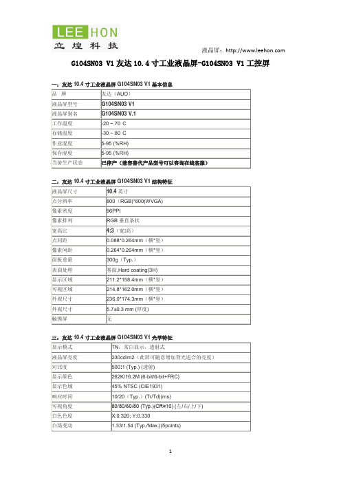
一:友达10.4寸工业液晶屏G104SN03 V1基本信息
品牌
友达(AUO)
液晶屏型号
G104SN03 V1
液晶屏别名
G104SN03 V.1
工作温度
-20 ~ 70°C
存储温度
-30 ~ 80°C
作业湿度
5-95 (%RH)
保存湿度
5-95 (%RH)
当前生产状态
已停产(兼容替代产品型号可以咨询在线客服)
白色色度
X:0.320; Y:0.330
白场变动
1.33/1.54 (Typ./Max.)(5points)
四、友达10.4寸工业液晶屏G104SN03 V1光系统
灯管位置
侧入式光源
光源类型
CCFL
灯管形状
直线
光源寿命
30K(Typ.)(小时)
单灯电压
540V (Typ./Max.)
单灯电流
3.0/4.5/5.5mA (Min./Typ./Max.)
端子
接口脚距
1.0mm
接口数量
1pcs
接口脚数
20pins
●补充说明:以上友达10.4寸工业液晶屏G104SN03 V1资料仅供参考,如有某项不准确,可以联系我们客服提供产品G104SN03 V1的规格资料,产品均以pdf规格为准。
电阻触摸屏、电容触摸屏选型:/Touch-screen/
灯管总功率
2.43W (Typ.)
接口类型
端子
背光电路
无
五、友达10.4寸工业液晶屏G104SN03 V1信号接口
信号大类
LVDS
信号小类
LVDS(1 ch, 6/8-bit)
TFT-LCD Approval Spec G104X1-L04 奇美10.4寸规格书-杭州旭虹科技

Note (1) Temperature and relative humidity range is shown in the figure below.
(b) Wet-bulb temperature should be 39 ºC Max. (Ta > 40 ºC). (c) No condensation
工业液晶屏www.hzxuhong.com
1.5 MECHANICAL SPECIFICATIONS
Item Horizontal (H) Module Size Vertical (V) Depth (D) Weight Min. 225 175.8 8.2 380 Typ. 225.5 176.3 8.7 430 Max. 226 176.8 9.2 480 Unit mm mm mm g
2.2.2 LED CONVERTER
Item Converter Voltage Enable Voltage Backlight Adjust Symbol Vi EN ADJ Value Min. -0.3 ----Max. 18 5.5 3.3 Unit V V V Note (1), (2)
Customer: Approved by: Note:
®Ö-ã ɶ¡ 2010-09-24 17:56:08
³¡ªù APPL ²£«~ºÞ²z³B
¼f®Ö ±i³ëµ¾
¨¤¦â Director
§ë²¼ Accept
1/26
Version 2.3
友达奇美群创京东方液晶屏代理商-杭州旭虹科技
Issued Date: Sep. 10, 2010 Model No.: G104X1-L04
Approval
TM097TDHG04-00 V1.3-杭州旭虹科技有限公司
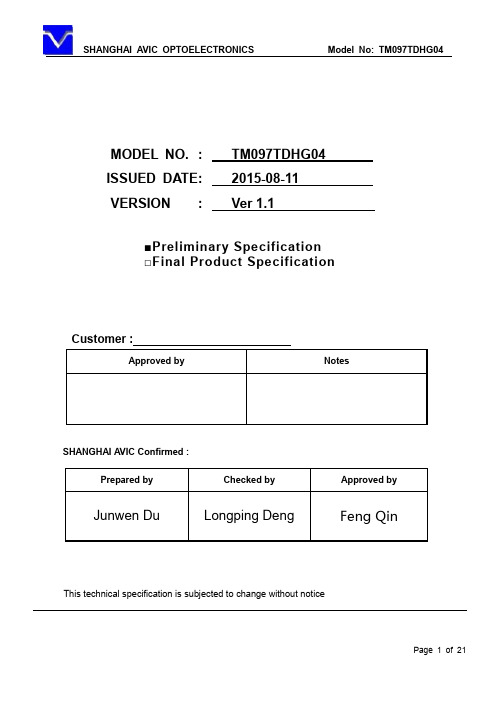
MODEL NO. : TM097TDHG04 ISSUED DATE: 2015-08-11 VERSION : Ver 1.1■Preliminary Specification □Final Product SpecificationCustomer :SHANGHAI AVIC Confirmed :This technical specification is subjected to change without notice工业液晶屏www.hzxuhong.com/杭州旭虹科技有限公司Table of ContentsTable of Contents (2)Record of Revision (3)1 General Specifications (4)2 Input/Output Terminals (5)3 Absolute Maximum Ratings (6)4 Electrical Characteristics (7)5 Timing Chart (10)6 Optical Characteristics (15)7 Environmental / Reliability Test (18)8 Mechanical Drawing (19)9 Packing drawing (20)10 Precautions for Use of LCD Modules (21)Record of RevisionNote 1: Viewing direction for best image quality is different from TFT definition. There is a 180 degree shift.Note 2: Requirements on Environmental Protection: RoHSNote 3: LCM weight tolerance: +/- 5%杭州旭虹科技有限公司2.1 CN1 of FPCNote: I/O definition.I---Input pin,O---Output pin,P--- Power/Ground,N--- No Connection 杭州旭虹科技有限公司3 Absolute Maximum Ratings工业液晶屏www.hzxuhong.com/工业液晶屏www.hzxuhong.com/4 Electrical Characteristics4.1 Recommended Operating Condition工业液晶屏www.hzxuhong.com/4.2 Recommended Driving Condition for BacklightNote1: For each LED: I F (1/6) =20mA, V F (1/6) =3.2V.Note2: Under LCM operating, the stable forward current should be inputted. And forward voltage is for reference only.Note3: I F is defined for one channel LED. Optical performance should be evaluated at Ta=25℃only If LED is driven by high current, high ambient temperature & humidity condition. The life time of LED will be reduced. Operating life means brightness goes down to 50% initial brightness. Typical operating life time is estimated data.Note4: The LED driving condition is defined for each LED module.杭州旭虹科技有限公司4.3 Power Consumption杭州旭虹科技有限公司工业液晶屏www.hzxuhong.com/5 Timing Chart5.1 TFT-LCD Input TimingDC specification工业液晶屏www.hzxuhong.com/杭州旭虹科技有限公司AC specification工业液晶屏www.hzxuhong.com/杭州旭虹科技有限公司工业液晶屏www.hzxuhong.com/杭州旭虹科技有限公司5.2 Timing Setting Of Signal Input Timing Of ConnectorDate input:杭州旭虹科技有限公司5.3 POWER ON/OFF SEQUENCE杭州旭虹科技有限公司6 Optical CharacteristicsT a=25℃Item Symbol Condition Min Typ Max Unit RemarkView Angles θTCR≧105060 -Degree Note 2 θB 60 70 -θL 60 70 -θR 60 70 -Contrast Ratio CR θ=0°400 500 - Note1 Note3Response Time T ON25℃- 20 25msNote1Note4 T OFFChromaticity WhitexBacklight ison0.258 0.308 0.358Note1Note5 y 0.269 0.319 0.369Redx 0.539 0.589 0.639y 0.301 0.351 0.401Greenx 0.299 0.349 0.399y 0.519 0.569 0.619Bluex 0.104 0.154 0.204y 0.033 0.083 0.133Uniformity U 75 -- % Note1 Note6NTSC 45 50 - % Note 5Luminance L 280 350 - cd/m2Note1 Note7Test Conditions:1. I F= 120 mA, V F=19.2 V and the ambient temperature is 25℃.2. The test systems refer to Note 1 and Note 2.工业液晶屏www.hzxuhong.com/杭州旭虹科技有限公司The optical characteristics should be measured in dark room. After 5 Minutes operation, the optical properties are measured at the center point of the LCD screen. All input terminals LCD panel must be ground when measuring the center area of the panel.Note 2: Definition of viewing angle range and measurement system.viewing angle is measured at the center point of the LCD by CONOSCOPE(ergo-80)。
AOC CU34G10X LCD液晶显示器用户手册说明书

液晶显示器用户说明书CU34G10X安全 (1)标志惯例 (1)电源 (2)安装 (3)清洁 (4)其它 (5)设置 (6)物品清单 (6)安装支架和底座 (7)调整视角 (8)连接显示器 (9)Adaptive-Sync功能 (10)HDR (11)调节显示器 (12)热键 (12)OSD设定 (13)Luminance(明亮度) (14)Color Setup(颜色设置) (15)Picture Boost(窗口增亮) (16)OSD Setup(OSD设置) (17)PIP Setting(PIP设置) (18)Game Setting(游戏设定) (19)Extra(其它) (20)Exit(退出) (21)LED指示灯 (22)故障排除 (23)规格 (24)主要规格 (24)预设显示模式 (25)引脚分配 (26)即插即用 (27)安全标志惯例以下小节描述此文档中使用的标志惯例。
注释、注意和警告在本指南中,文本块可能带有图标并且以粗体或斜体打印。
这些文本块是注释、注意和警告,如下所示:注释:注意事项指示帮助你更好地使用你的计算机系统的重要信息。
注意:“注意”表示潜在的硬件损坏或数据丢失,并告诉您如何避免出现问题。
警告:“警告”表示存在潜在的人身伤害,并告诉您如何避免伤害的发生。
某些警告可能采用其它格式,也可能不带有图标。
在这种情况下,由相关的管制机构提供专门的警告表示方法。
显示器应使用铭牌上标示的电源规格。
如果您不能确定家里电源规格,请咨询供应商或当地电力公司。
显示器配备三项接地插头,一个插头具有第三个(接地)引脚。
这个引脚会只嵌入作为安全装置的接地电源插座。
如果插座不适合三线插头,那么请让电工安装正确的插座,或者使用转接器使得仪器安全接地。
请不要使接地插头的安全目的失效。
在雷雨天气或者当长期不用时请拔掉电源插头。
这可以保护显示器不会因为电压剧烈变化而遭到损坏。
请勿使电源插座和外接电源线过载。
- 1、下载文档前请自行甄别文档内容的完整性,平台不提供额外的编辑、内容补充、找答案等附加服务。
- 2、"仅部分预览"的文档,不可在线预览部分如存在完整性等问题,可反馈申请退款(可完整预览的文档不适用该条件!)。
- 3、如文档侵犯您的权益,请联系客服反馈,我们会尽快为您处理(人工客服工作时间:9:00-18:30)。
( V ) Preliminary Specifications( ) Final SpecificationsModule 10.4 Inch Color TFT-LCD Model Name G104XVN01.0Customer DateChecked &Approved byNote: This Specification is subject to changewithout notice. Approved by DateLeader Feng 2010/7/15 Prepared byYichih Chen 2010/7/15 General Display Business Division / AU Optronics corporationContents1. Operating Precautions (4)2. General Description (5)2.1 Display Characteristics (5)2.2 Optical Characteristics (6)3. Functional Block Diagram (9)4. Absolute Maximum Ratings (10)4.1 Absolute Ratings of TFT LCD Module (10)4.2 Absolute Ratings of Environment (10)5. Electrical Characteristics (11)5.1 TFT LCD Module (11)5.2 Backlight Unit (13)6. Signal Characteristics (14)6.1 Pixel Format Image (14)6.2 Scanning Direction (14)6.3 TFT-LCD Interface Signal Description (15)6.4 The Input Data Format (16)6.5 TFT-LCD Interface Timing (17)6.6 Power ON/OFF Sequence (18)7. Connector & Pin Assignment (19)7.1 TFT-LCD Signal (CN1): LVDS Connector (19)7.2 LED Backlight Unit (CN2): Driver Connector (19)7.3 LED Backlight Unit (CN4): Light bar Connector (19)8. Reliability Test Criteria (20)9. Mechanical Characteristics (21)9.1 LCM Outline Dimension (Front View) (21)9.2 LCM Outline Dimension (Rear View) (22)10. Label and Packaging (23)10.1 Shipping Label (on the rear side of TFT-LCD display) (23)10.2 Carton Package (23)11 Safety (24)11.1 Sharp Edge Requirements (24)11.2 Materials (24)11.3 Capacitors (24)11.4 National Test Lab Requirement (24)Record of RevisionVersion and Date Page Old descriptionNew Description0.0 2012/07/15 AllFirst Edition1. Operating Precautions1) Since front polarizer is easily damaged, please be cautious and not to scratch it.2) Be sure to turn off power supply when inserting or disconnecting from input connector.3) Wipe off water drop immediately. Long contact with water may cause discoloration orspots.4) When the panel surface is soiled, wipe it with absorbent cotton or soft cloth.5) Since the panel is made of glass, it may be broken or cracked if dropped or bumped onhard surface.6) To avoid ESD (Electro Static Discharde) damage, be sure to ground yourself before handlingTFT-LCD Module.7) Do not open nor modify the module assembly.8) Do not press the reflector sheet at the back of the module to any direction.9) In case if a module has to be put back into the packing container slot after it was takenout from the container, do not press the center of the LED light bar edge. Instead, press at the far ends of the LED light bar edge softly. Otherwise the TFT Module may be damaged.10) At the insertion or removal of the Signal Interface Connector, be sure not to rotate nortilt the Interface Connector of the TFT Module.11) TFT-LCD Module is not allowed to be twisted & bent even force is added on module in a veryshort time. Please design your display product well to avoid external force applying to module by end-user directly.12) Small amount of materials without flammability grade are used in the TFT-LCD module. TheTFT-LCD module should be supplied by power complied with requirements of Limited Power Source (IEC60950 or UL1950), or be applied exemption.13) Severe temperature condition may result in different luminance, response time and lampignition voltage.14) Continuous operating TFT-LCD display under low temperature environment may acceleratelamp exhaustion and reduce luminance dramatically.15) The data on this specification sheet is applicable when LCD module is placed in landscapeposition.16) Continuous displaying fixed pattern may induce image sticking. It’s recommended to usescreen saver or shuffle content periodically if fixed pattern is displayed on the screen.2. General DescriptionThis specification applies to the Color Active Matrix Liquid Crystal Display G104XVN01.0composed of a TFT-LCD display, a driver and power supply circuit, and a LED backlight system. The screen format is intended to support XGA (1024(H) x 768(V)) screen and 16.2M (RGB 8-bits) or 262k colors (RGB 6-bits).LED driving board for backlight unit is included in G104XVN01.0.G104XVN01.0 designed with wide viewing angle; wide temperature and long life LED backlight is well suited for industial applications. G104XVN01.0 is a RoHS product.2.1 Display CharacteristicsThe following items are characteristics summary on the table under 25 ℃ condition: ItemsUnitSpecifications Screen Diagonal [inch] 10.4Active Area [mm] 210.4 (H) x 157.8 (V) Pixels H x V 1024 x 3(RGB) x 768 Pixel Pitch [mm] 0.2055 x 0.2055 Pixel Arrangement R.G.B. Vertical Stripe Display ModePSA, Normally Black Nominal Input Voltage VDD [Volt] 3.3 (typ.) Typical Power Consumption [Watt] 6.0WAll black pattern Weight [Grams] 350(Typ.)Physical Size [mm] 238.6(H) x 175.8(V) x 6.5(D)(Typ.) Electrical Interface 1 channel LVDS Surface Treatment Anti-glare, Hardness 3H Support Color16.2M / 262K colors Temperature Range OperatingStorage (Non-Operating) [o C] [o C]-30 to +80 -30 to +80 RoHS ComplianceRoHS Compliance2.2 Optical CharacteristicsThe optical characteristics are measured under stable conditions at 25 (Room Temperature):℃Item Unit Conditions Min. Typ. Max. Remark White Luminance[cd/m2] I F = 80mA/1 LED Line (center point) 300 400 -Note 1 Uniformity % 5 Points 75 80 -Note 2, 3 Contrast Ratio500 1400 - Note 4[msec]Rising - 20 30 [msec] Falling- 10 20 Response Time[msec] Raising + Falling - 30 50 Note 5 [degree] [degree] Horizontal (Right) CR = 10 (Left) - - 89 89 - - Viewing Angle[degree] [degree]Vertical (Upper) CR = 10 (Lower) - - 89 89 - - Note 6 Red x TBD TBD TBD Red y TBD TBD TBD Green xTBD TBD TBD Green y TBD TBD TBD Blue x TBD TBD TBD Blue y TBD TBD TBD White x 0.263 0.313 0.363 Color / ChromaticityCoordinates (CIE 1931)White y0.279 0.329 0.379 Color Gamut%-60-Note 1: Measurement method Equipment Pattern Generator, Power Supply, Digital Voltmeter, Luminance meter (SR_3 or equivalent) Aperture1with 50cm viewing distance ∘Test Point CenterEnvironment < 1 luxModule Driving EquipmentNote 2: Definition of 5 points position (Display active area: 210.4mm (H) x 157.8mm (V))Note 3: The luminance uniformity of 5 points is defined by dividing the minimum luminance values by the maximum test point luminanceNote 4: Definition of contrast ratio (CR):Note 5: Definition of response time:The output signals of photo detector are measured when the input signals are changed from “White” to “Black” (falling time) and from “Black” to “White” (rising time), respectively. The response time interval isNote 6: Definition of viewing angleViewing angle is the measurement of contrast ratio 10, at the screen center, over a 180° horizontal and ≧180° vertical range (off-normal viewing angles). The 180° viewing angle range is broken down as below: 90° (θ) horizontal left and right, and 90° (Φ) vertical high (up) and low (down). The measurement direction is typically perpendicular to the display surface with the screen rotated to its center to develop the desiredMinimum Brightness of five pointsδW9 = Maximum Brightness of five points Contrast ratio (CR)=Brightness on the “White” stateBrightness on the “Black” statemeasurement viewing angle.3. Functional Block DiagramThe following diagram shows the functional block of the 10.4 inch color TFT/LCD module:4. Absolute Maximum Ratings4.1 Absolute Ratings of TFT LCD ModuleItem Symbol Min Max Unit Logic/LCD Drive Voltage Vin -0.3 6 [Volt]4.2 Absolute Ratings of EnvironmentItem Symbol Min Max Unit Operating Temperature TOP -30 +80 [o C] Operation Humidity HOP 5 95 [%RH] Storage Temperature TST -30 +80 [o C] Storage Humidity HST 5 95 [%RH] Note: Maximum Wet-Bulb should be 39℃ and no condensation.5. Electrical Characteristics 5.1 TFT LCD Module5.1.1 Power SpecificationSymbol Parameter Min Typ Max Units RemarkVDD Logic/LCD Input Voltage 3.1 3.3 3.5 [Volt]I VDD LCD Input Current - 200 - [mA]VDD=3.3V at 60 HZ, all Black PatternP VDD LCD Power comsumption - 0.99 -[Watt] VDD=3.3V at 60 HZ, all Black Pattern I rush LCDLCD Inrush Current-- 1.5[A] Note 1; VDD=3.3VBlack Pattern, Rising time=470usVDD rpAllowable Logic/LCDDrive Ripple Voltage- -100[mV] p-pVDD=3.3V at 60 HZ, all Black PatternNote 1: Measurement condition:VDD rising time0V3.3V5.1.2 Signal Electrical CharacteristicsInput signals shall be low or Hi-Z state when VDD is off.Note: LVDS Signal Waveform.SymbolItemMin. Typ. Max. Unit RemarkVTH Differential Input High Threshold - - 100 [mV] VCM=1.2V VTL Differential Input Low Threshold 100 - - [mV] VCM=1.2V |VID |Input Differential Voltage100 400 600 [mV] VICMDifferential Input Common Mode Voltage1.1-1.45[V]VTH/VTL=+-100mV5.2 Backlight Unit5.2.1 Parameter guideline for LED backlightFollowing characteristics are measured under a stable condition using a inverter at 25℃. (Room Temperature): Symbol Parameter Min.Typ.Max.Unit RemarkVCC Input Voltage 10.8 12 12.6 [Volt]I VCC Input Current - 0.5 - [A] 100% PWM DutyP VCC Power Consumption - 6 - [Watt] 100% PWM DutyI INRUSH LED Inrush Current - - 3 A V LED rising time ~ 470usF PWM Dimming Frequency 200 - 20K [Hz]On Control Voltage 2.5 3.3 5.5 VoltNote 4,5 V LED ON/OFFOff Control Voltage - - 0.8 Volt[Volt]VPWM DIM Swing Voltage 2.5 3.3 5.5Dimming duty cycle 5 - 100 %I F LED Forward Current-80 -[mA] Ta = 25o C- - - [Volt]I F = 80mA, Ta = -30o C V F LED Forward Voltage- 29.7 32.4 [Volt]I F = 80mA, Ta = 25o C- - - [Volt]I F = 80mA, Ta = 85o C P LED LED Power Consumption- 4.75 - [Watt] 2 String of LED Light Bar Operation Life 50,000 - - Hrs I F=80mA, Ta= 25o CNote 1: Ta means ambient temperature of TFT-LCD module.Note 2: VCC, I VCC, I rush LED, P VCC are defined for LED backlight.(100% duty of PWM dimming)Note 3: I F, V F are defined for one channel LED. There are two LED channel in back light unit.Note 4: PWM dimming function can be operated by PWM signal. PWM duty cycle can adjust white Luminance.(PWM High: ON and PWM Low: OFF)Note 5: PWM signal can not be floating and pull-down to ground when waiting.Note 6: If G104XVN01.0 module is driven by high current or at high ambient temperature & humidity condition. The operating life will be reduced.Note 7: Operating life means brightness goes down to 50% initial brightness. Minimum operating life time is estimated data.6. Signal Characteristics6.1 Pixel Format ImageFollowing figure shows the relationship between input signal and LCD pixel format.1st2nd1023th1024th1stLine768thLin6.2 Scanning DirectionThe following figures show the image seen from the front view. The arrow indicates the direction of scan.Fig. 1 Normal scan (Pin24, Reverse = Low or NC) Fig. 2 Reverse scan (Pin24, Reverse = High)6.3 TFT-LCD Interface Signal DescriptionThe module using a LVDS receiver embaded in AUO’s ASIC. LVDS is a differential signal technology for LCD interface and a high-speed data transfer device.Pin No. Signal Name Description1 NC No Connection2 GND Ground3 Rin3+ Positive LVDS differential data input (+)4 Rin3- Negative LVDS differential data input (-)5 GND Ground6 CLK+ Clock signal (+)7 CLK- Clock signal (-)8 GND Ground9 Rin2+ Positive LVDS differential data input (+)10 Rin2- Negative LVDS differential data input (-)11 GND Ground12 Rin1+ Positive LVDS differential data input (+)13 Rin1- Negative LVDS differential data input (-)14 GND Ground15 Rin0+ Positive LVDS differential data input (+)16 Rin0- Negative LVDS differential data input (-)17 GND Ground18 NC No Connection19 GND Ground20 SEL6/8 Selection for 6 bits/8bits LVDS data input Low or NC ->8 bit Input ModeHigh ->6bit Input Mode21 NC No Connection22 NC No Connection23 NC No Connection24 Reverse Reverse Panel Function (Display Rotation)25 GND Ground26 GND Ground27 GND Ground28 VCC Power supply: +3.3V29 VCC Power supply: +3.3V30 VCC Power supply: +3.3VNote 1: Input Signals shall be in low status when VDD is off.Note 2: High stands for “3.3V”, Low stands for “0V”, NC stands for “No Connection”.Note 3: RSV stands for “Reserved”.6.4 The Input Data Format6.4.1 SEL68SEL68 = “High” for 6 bits LVDS InputSEL68 = “Low” or “NC” for 8 bits LVDS InputNote1: Please follow PSWG.Note2:R/G/B data 7:MSB, R/G/B data 0:LSB Signal NameDescription RemarkR7 R6 R5 R4 R3 R2 R1 R0 Red Data 7Red Data 6Red Data 5Red Data 4Red Data 3Red Data 2Red Data 1Red Data 0Red-pixel DataFor 8Bits LVDS inputMSB: R7 ; LSB: R0For 6Bits LVDS inputMSB: R5 ; LSB: R0G7 G6 G5 G4 G3 G2 G1 G0 Green Data 7Green Data 6Green Data 5Green Data 4Green Data 3Green Data 2Green Data 1Green Data 0Green-pixel DataFor 8Bits LVDS inputMSB: G7 ; LSB: G0For 6Bits LVDS inputMSB: G5 ; LSB: G0B7 B6 B5 B4 B3 B2 B1 B0 Blue Data 7Blue Data 6Blue Data 5Blue Data 4Blue Data 3Blue Data 2Blue Data 1Blue Data 0Blue-pixel DataFor 8Bits LVDS inputMSB: B7 ; LSB: B0For 6Bits LVDS inputMSB: B5 ; LSB: B0RxCLKIN LVDS Data ClockDE Data Enable Signal When the signal is high, the pixel datashall be valid to be displayed.Note: Output signals from any system shall be low or Hi-Z state when VDD is off.NS-like format6.5 TFT-LCD Interface Timing6.5.1 Timing CharacteristicsSignal Symbol Min. Typ. Max. Unit Clock Frequency 1/ T Clock 50 65 81 MHzPeriod T V 776 806 1023 Active T VD 768 768768 Vertical SectionBlankingT VB 8 38 256 T Line Period T H 1054 13442047 Active T HD 1024 1024 1024 Horizontal SectionBlankingT HB 30 320 1023 TClock Frame RateF 506075Hz Note : DE mode.6.5.2 Input Timing DiagramDOTCLKDEHT HBDET VDInput Timing Definition ( DE Mode)Input Data Invaild Data Invaild Data6.6 Power ON/OFF SequenceVDD power and lamp on/off sequence is as below. Interface signals are also shown in the chart. Signals from any system shall be Hi-Z state or low level when VDD is off.Power ON/OFF sequence timingValue UnitsParameterMin. Typ. Max.T10.5 - 10 [ms]T2 30 40 50 [ms]T3 200 -- -- [ms]T4 0.5 -- 10 [ms]T5 10 - - [ms]T6 10 - - [ms]T7 0 - - [ms]T8 10 - - [ms]T9 -- -- 10 [ms]T10 110 -- -- [ms]T11 0 16 50 [ms]T12 - - 10 [ms]T13 1000 - - [ms]The above on/off sequence should be applied to avoid abnormal function in the display. Please make sure to turn off the power when you plug the cable into the input connector or pull the cable out of the connector.7. Connector & Pin AssignmentPhysical interface is described as for the connector on module. These connectors are capable of accommodating the following signals and will be following components.7.1 TFT-LCD Signal (CN1): LVDS ConnectorConnector Name / Designation Signal ConnectorManufacturer JAE or compatibleConnector Model Number FI-XPB30SRLAHF11or compatibleAdaptable Plug FI-X30HL or Compatible or compatiblePin No. Symbol Pin No. Symbol1 NC 16 Rin0-2 GND 17 GND3 Rin3+ 18 NC4 Rin3- 19 GND5 GND 20 SEL6/86 CLK+ 21 NC7 CLK- 22 NC8 GND 23 NC9 Rin2+ 24 Reverse10 Rin2- 25 GND11 GND 26 GND12 Rin1+ 27 GND13 Rin1- 28 VCC14 GND 29 VCC15 Rin0+ 30 VCC7.2 LED Backlight Unit (CN2): Driver ConnectorConnector Name / Designation Lamp ConnectorManufacturer ENTERY or compatibleConnector Model Number 3808K-F05N-02R or compatibleMating Model Number H208K–P05N-02B or compatiblePin No. symbol descriptionPin1 VCC 12V inputPin2 VCC 12V inputPin3 GND GNDPin4 Dimming PWMPin5 On/OFF 3.3V or 5V-ON,0V-OFF7.3 LED Backlight Unit (CN3): Light bar ConnectorConnector Name / Designation Lamp ConnectorManufacturer ENTERY or compatibleConnector Model Number H208K–P03N-02R or compatibleMating Model Number(CN3) 3808K-F03N-02B or compatiblePin No. symbol description ColorPin1 H LED anode RedPin2 L LED cathode WhitePin3 L LED cathode White8. Reliability Test CriteriaItems Required Condition Note Temperature Humidity Bias 40℃, 90%RH, 300 hoursHigh Temperature Operation 80℃, 300 hoursLow Temperature Operation -30℃, 300 hoursHot Storage 80,℃ 300 hoursCold Storage -30℃, 300 hoursThermal Shock Test -20/℃ 30 min, 60/℃ 30 min, 100cycles, 40℃minimun ramp rateHot Start Test 80℃/ 1Hr min. power on/off per 5 minutes, 5 timesCold Start Test -30℃/ 1Hr min. power on/off per 5 minutes, 5 timesShock Test (Non-Operating) 50G, 20ms, Half-sine wave, ( ±X, ±Y, ±Z)Vibration Test (Non-Operating) 1.5G, (10~200Hz, Sine wave)30 mins/axis, 3 direction (X, Y, Z)On/off test On/10 sec, Off/10 sec, 30,000 cyclesESD Contact Discharge: ± 8KV, 150pF(330Ω ) 1sec, 8 points, 25 times/ pointAir Discharge: ± 15KV, 150pF(330Ω ) 1sec, 8 points, 25 times/ pointNote 1EMI 30-230 MHz, limit 40 dBu V/m, 230-1000 MHz, limit 47 dBu V/mNote1: According to EN61000-4-2, ESD class B: Some performance degradation allowed. No data lost Self-recoverable. No hardware failures.Note2:Water condensation is not allowed for each test items.Each test is done by new TFT-LCD module. Don’t use the same TFT-LCD module repeatedly for reliability test. The reliability test is performed only to examine the TFT-LCD module capability.To inspect TFT-LCD module after reliability test, please store it at room temperature and room humidity for 24 hours at least in advance.9. Mechanical Characteristics9.1 LCM Outline Dimension (Front View)9.2 LCM Outline Dimension (Rear View)10. Label and Packaging10.1 Shipping Label (on the rear side of TFT-LCD display)10.2 Carton PackageNote:1. Max. Capacity: 40pcs LCD Modules / per carton2. Max. Weight: 14.5 kg / per carton3. The outside dimension of carton is 458(L) mm x 412(W) mm x 368(H) mm11 Safety11.1 Sharp Edge RequirementsThere will be no sharp edges or comers on the display assembly that could cause injury.11.2 Materials11.2.1 ToxicityThere will be no carcinogenic materials used anywhere in the display module. If toxic materials are used, they will be reviewed and approved by the responsible AUO toxicologist.11.2.2 FlammabilityAll components including electrical components that do not meet the flammability grade UL94-V1 in the module will complete the flammability rating exception approval process.The printed circuit board will be made from material rated 94-V1 or better. The actual UL flammability rating will be printed on the printed circuit board.11.3 CapacitorsIf any polarized capacitors are used in the display assembly, provisions will be made to keep themfrom being inserted backwards.11.4 National Test Lab RequirementThe display module will satisfy all requirements for compliance to:UL 1950, First Edition U.S.A. Information Technology Equipment。