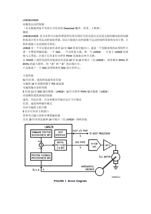
LM628-LM629 高精度运动控制器 国家半导体公司
fp6296规格书

fp6296规格书摘要:一、前言二、FP6296 芯片概述1.产品简介2.主要特性三、FP6296 功能模块介绍1.电源管理模块2.音频处理模块3.显示处理模块4.通信接口模块四、FP6296 应用领域1.消费类电子产品2.工业控制领域3.医疗设备五、FP6296 技术支持与服务1.技术支持2.售后服务六、结语正文:【前言】FP6296 是一款高性能的芯片,广泛应用于各种电子产品中。
本文将对FP6296 的规格书进行详细解读,帮助大家更好地了解这款芯片。
【FP6296 芯片概述】【产品简介】FP6296 是一款集成了电源管理、音频处理、显示处理和通信接口等多种功能的高性能芯片。
它具有高度集成、低成本、易于应用等特点,可满足各类电子产品的需求。
【主要特性】1.高度集成:集成了多种功能模块,减少了外部元器件数量,节省了电路板空间。
2.性能优异:具备高效、稳定的性能,满足各类电子产品的运行需求。
3.兼容性强:支持多种通信接口和显示标准,便于与各类外部设备连接。
【FP6296 功能模块介绍】【电源管理模块】电源管理模块负责对整个系统的电源进行监控和控制,保证系统稳定运行。
具有自动调整输出电压、电流的功能,以适应不同负载需求。
【音频处理模块】音频处理模块提供高质量的音频信号处理功能,包括音频放大、滤波、降噪等,适用于各类音频设备。
【显示处理模块】显示处理模块支持多种显示标准,能够实现高清视频的解码和显示,适用于电视、显示器等设备。
【通信接口模块】通信接口模块支持多种通信协议,如USB、HDMI、SD 卡等,方便与外部设备连接,进行数据传输。
【FP6296 应用领域】【消费类电子产品】FP6296 广泛应用于智能手机、平板电脑、数码相机等消费类电子产品中,提供稳定的性能支持。
【工业控制领域】FP6296 在工业控制领域也有广泛应用,如自动化生产线、智能家居等,为各类设备提供核心控制功能。
【医疗设备】FP6296 在医疗设备中也有重要应用,如心电图仪、超声波设备等,保证医疗设备的高效、稳定运行。
LM628-LM629_高精度运动控制器_国家半导体公司
输出电平 VOH 逻辑 1 VOL IOUT 逻辑 0 三态输出漏电流
交流电气规格 (VDD 和 TA 符合操作范围,FCLK=6MHz,CLOAD=50pF,Input Test Signal tr=tf=10ns) T# 定时间隔 测试极限 单位
最小 编码器和索引时间(见 Figure 2) 电机-相脉宽 每个状态的保持时间 索引脉冲的设置和保持 (对于 A 高 B 低) 时钟和复位时间(见 Figure 3) 时钟脉宽 LM628N-6,LM629N-6,LM629M-6 LM628N-8,LM629N-8,LM629M-8 时钟周期 LM628N-6,LM629N-6,LM629M-6 LM628N-8,LM629N-8,LM629M-8 复位脉宽 状态字读取时间(见 Figure 4) 片选设置/保持时间 端口选择的设置时间 端口选择的保持时间 读数据进入时间 读数据保持时间 /RD 高电平到 Hi-Z 时间 指令字写时间(见 Figure 5) 片选设置/保持时间 端口选择的设置时间 端口选择的保持时间 Busy 位延时 /WR 脉宽 写数据设置时间 写数据保持时间 数据双字读取时间(见 Figure 6) 片选设置/保持时间 端口选择的设置时间 端口选择的保持时间 读数据进入时间 读数据保持时间 /RD 高电平到 Hi-Z 时间 Busy 位延时 读取恢复时间 数据双字写如时间(见 Figure 7) 片选设置/保持时间 端口选择的设置时间 端口选择的保持时间 Busy 位延时 T7 T8 T9 T13 0 30 30 T7 T8 T9 T10 T11 T12 T13 T17 120 0 0 30 30 T7 T8 T9 T13 T14 T15 T16 100 50 120 0 30 30 T7 T8 T9 T10 T11 T12 0 0 30 30 T4 T4 T5 T5 T6 78 57 166 125 8/fCLK T1 T2 T3 16/fCLK 8/fCLK 0
T6290综测仪产品介绍

T6290
标准差(整体)/(组内) 0.44/0.66 0.18/0.22 0.25/0.64 0.15/0.35 0.11/0.34 0.13/0.19 0.13/0.17 0.11/0.25 0.22/0.43 0.47/0.72 0.36/0.36 0.33/0.51 0.12/0.25 0.50/0.72 0.21/0.26
北京公司: 朝阳区中化地质大厦一层 研发中心
上海总部: 松江区新飞路1500号26栋 生产制造、质量控制
深圳公司: 南山区桃源街道田寮大厦1208 销售、技术支持、仓储、物流
产业经历
T6290申请10项发明专利保护
2014重组成立为准电子,推出T6290产线型综测 仪,并实现规模量产应用 2014年国家重大专项全模综测仪项目 2013年实现LTE/TD/W/GGE多模综测仪产线规模应用 2012年TDD/FDD-LTE综测仪平台发布, TDD/FDD LTE Advanced功能开发 2011年T6280多模信令综测仪发布 2010年LTE/WCDMA/GGE开发。 2009年综测仪在TD生产线规模应用(300台)
• 工厂采购在仪表高峰期从多家仪表租赁商租用仪表,不同厂家CMW500的版本,精
解决工厂租用仪表 的品质保障及一站 式获得解决方案
准度,软件盗版问题,仪表年度校准维护参差不齐,无法管理。 •各租赁厂商提供的测试配件品质堪忧 •T6290租赁仪表每半年原厂检查和校准一次,出库前使用高级源测试指标,保障仪表 的精准性,仪表品质,可用数量,技术支持能力,极大解决由于采购鱼目混杂的租赁 源头的仪表品质不确定和混乱,引发的生产可靠性保障问题
• 与德与振华工厂战略合作,4G项目全线采用T6290生产,在振华长期保持100台左右 的使用量,为魅族,中兴,宇龙,HTC项目做生产,客户反馈良好,得到各界高度 信任。 • ONTIM与中诺工厂ODM华为的项目全线采用T6290生产,中诺及其外协厂(光弘, 德邦)长期保持100台左右的使用量,性能稳定。生产的华为“畅享5”项目获中国 移动2015年千元智能机项目质量第一名。 • 华勤给华为的ODM项目在长城开发虎门新厂的项目自2015年底导入T6290以来,受 到客户的一致好评,目前T6290在该厂保持60台左右的使用量,并不断增加。 • 德赛4G产线指定使用T6290仪表,为TCL/ACTEL,天珑等生产,随着4G产品比重加大, 目前已经增加至30台以上。
运动控制器的应用现状及其发展趋势【不可外传】
运动控制器的应用现状及其发展趋势内容来源网络,由“深圳机械展(11万㎡,1100多家展商,超10万观众)”收集整理!更多cnc加工中心、车铣磨钻床、线切割、数控刀具工具、工业机器人、非标自动化、数字化无人工厂、精密测量、数控系统、3D打印、激光切割、钣金冲压折弯、精密零件加工等展示,就在深圳机械展.1运动控制器的应用现状运动控制器越来越广泛地应用于各个行业的自动化设备,如数控机床、雕刻机、切割机、钻孔机、印刷机、冲孔机、激光雕刻、激光切割、包装机、纺织机、食品加工、绘图机、点胶机、焊接机、电子装配白动检测等,甚至在航空航天和国防领域也得到广泛应用。
根据所用的CPU不同,运动控制器产品主要有以下五种类型:(1)以单片机(MCU)为核心的运动控制器,低端采用8位或16位的单片机作为处理器,其主要优点是价格比较低廉,缺点是运行速度较慢,控制精度较低。
因此这种运动控制器适用于一些低速或运动控制精度要求不高的点位运动或轮廓运动控制的自动化设备。
(2)以专用芯片为核心的运动控制器,美国国家半导体公司生产的LM628和LM629专用运动控制芯片,日本的NOVA生产的MCX304、MCX501等运动控制芯片是专门为精密控制步进电机和伺服电机而设计的专用处理器,产品应用于数控机床、雕刻机、工业机器人、医用设备、绕线机、自动仓库、绘图仪、点胶机、IC制造设备等领域。
(3)以数字信号处理器(DS)为核心的运动控制器,美国DeltaTau公司生产的PMAC 运动控制器,采用Motorola的DSP56003作为处理器。
国内的基于DSP的运动控制器,通常以美国TI公司推出的C2000系列,例如TMS320F2812和TMS320F28335作为运动控制器的核心芯片。
(4)基于SOPC技术的运动控制器,System-on-a-Programmable-Chip(SOPC),即可编程片上系统,这种运动控制器主要有两种类型:基于FPGA嵌入IP硬核的SOPC系统和基于FPGA嵌入IP软核的SOPC系统,如Altera公司推出的采用了哈佛结构、具有32位指令集成的第二代片上可编程的软核和硬核处理器。
华上芯片介绍
Dongguan Guangsu opto-electronics Co., Ltd.
产 品 介 绍
华上芯片 颜色 芯片型号:
尺 寸 波 长 亮度mcd 电压v
华上芯片 颜色 芯片型号:
尺 寸
波 长
亮度mcd 360-400
电压v
320-360 AOC-612RMM 620-627 红 主推 12miL 360-400 <2.4 光
<2.4
大功率产品
芯片型号:
规格
波长及亮度
电压
<2.7
备注
AOC-541RMM AOC-541YSM
大功率1W红光芯片 (华上) 大功率1W黄光芯片 (华上) 大功率1W红光芯片 (华上) 大功率1W红光芯片 (华上双线)
41*41miL 主推
620-627/7800(mcd)以上 587-592/6600(mcd)以上
公司主页: / 华上光电网址:/电话+886-3-3803801
联系人 :赵凯
13410238513
3500023
0769-81603478 版权所有
0769-89032879
©2012 Dongguan Guangsu.opto-electronics Co., Ltd.
AOC-S09RMM 主推
<2.4
320-360 460-520 <2.4 520-600
黄 光
AOC-S10YSM 9miL 587-592 主推
<2.4
320-360
红 AOC-614RMM 14miL 620-627 光
红 光 双 线 尺寸
AOC-H14RMM 14miL 620-630
北京联盛德微电子有限责任公司W601芯片规格书说明书

W601芯片规格书V1.0.4北京联盛德微电子有限责任公司 (Winner Micro)地址:北京市海淀区阜成路67号银都大厦18层电话:+86-10-62161900网址:文档历史目录1特征 (1)2概述 (4)3芯片特点 (4)4芯片结构 (4)5功能描述 (4)5.1SDIO设备控制器 (4)5.2高速SPI设备控制器 (5)5.3DMA控制器 (5)5.4时钟与复位 (5)5.5内存管理器 (5)5.6数字基带 (5)5.7MAC控制器 (6)5.8安全系统 (6)5.9FLASH控制器 (6)5.10RSA加密模块 (7)5.11通用硬件加密模块 (7)5.12I2C控制器 (7)5.13SAR ADC (7)5.14主/从SPI控制器 (7)5.15UART控制器 (8)5.16GPIO控制器 (8)5.17定时器 (8)5.18看门狗控制器 (8)5.19射频配置器 (8)5.20射频收发器 (8)5.21PWM控制器 (9)5.22I²S控制器 (9)5.237816/UART控制器 (9)5.24LCD控制器 (10)6管脚定义 (11)7电气特性 (14)7.1极限参数 (14)7.2射频功耗参数 (14)7.3Wi-Fi射频 (14)8封装信息 (16)1特征⚫芯片外观➢QFN68封装,7mm x 7mm⚫芯片集成度◼MCU 特性➢集成32位嵌入式Cortex-M3处理器,工作频率80MHz,内置1MB Flash,288KB RAM;➢集成3路UART 高速接口,波特率范围1200bps~2Mbps;➢集成8路10比特差分 ADC;➢集成1个SPI主从控制器,支持速率20MHz➢集成1个高速SPI从设备接口,支持最高50MHz;➢集成1个SDIO控制器,支持最高50MHz;➢集成1个I2C控制器,支持100/400Kbps 速率;➢集成GPIO控制器,支持48位可控GPIO;➢集成5路PWM接口;➢集成I2S控制器;➢集成7816接口,支持EVM2000规范,兼容串口功能;➢集成LCD控制器,最高支持4x20/8x16接口,支持2.7V~3.6V电压输出。
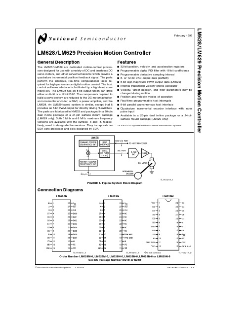
LM628-datasheet
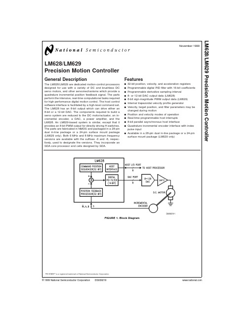
LM628/LM629Precision Motion ControllerGeneral DescriptionThe LM628/LM629are dedicated motion-control processors designed for use with a variety of DC and brushless DC servo motors,and other servomechanisms which provide a quadrature incremental position feedback signal.The parts perform the intensive,real-time computational tasks required for high performance digital motion control.The host control software interface is facilitated by a high-level command set.The LM628has an 8-bit output which can drive either an 8-bit or a 12-bit DAC.The components required to build a servo system are reduced to the DC motor/actuator,an in-cremental encoder,a DAC,a power amplifier,and the LM628.An LM629-based system is similar,except that it provides an 8-bit PWM output for directly driving H-switches.The parts are fabricated in NMOS and packaged in a 28-pin dual in-line package or a 24-pin surface mount package (LM629only).Both 6MHz and 8MHz maximum frequency versions are available with the suffixes -6and -8,respec-tively,used to designate the versions.They incorporate an SDA core processor and cells designed by SDA.Featuresn 32-bit position,velocity,and acceleration registers n Programmable digital PID filter with 16-bit coefficients n Programmable derivative sampling interval n 8-or 12-bit DAC output data (LM628)n 8-bit sign-magnitude PWM output data (LM629)n Internal trapezoidal velocity profile generatorn Velocity,target position,and filter parameters may be changed during motionn Position and velocity modes of operation n Real-time programmable host interrupts n 8-bit parallel asynchronous host interfacen Quadrature incremental encoder interface with index pulse inputnAvailable in a 28-pin dual in-line package or a 24-pin surface mount package (LM629only)TRI-STATE ®is a registered trademark of National Semiconductor Corporation.DS009219-1FIGURE 1.Block DiagramNovember 1999LM628/LM629Precision Motion Controller©1999National Semiconductor Corporation Connection DiagramsLM628NDS009219-2LM629NDS009219-3LM629MDS009219-21*Do not connect.Order Number LM629M-6,LM629M-8,LM628N-6,LM628N-8,LM629N-6or LM629N-8See NS Package Number M24B or N28BL M 628/L M 629 2Absolute Maximum Ratings(Note1)If Military/Aerospace specified devices are required, please contact the National Semiconductor Sales Office/ Distributors for availability and specifications.Voltage at Any Pin withRespect to GND−0.3V to+7.0V Ambient Storage Temperature−65˚C to+150˚C Lead Temperature28-pin Dual In-LinePackage(Soldering,4sec.)260˚C 24-pin Surface MountPackage(Soldering,10sec.)300˚C Maximum Power Dissipation(T A≤85˚C,(Note2)605mW ESD Tolerance(C ZAP=120pF,R ZAP=1.5k)2000V Operating RatingsTemperature Range−40˚C<T A<+85˚C Clock Frequency:LM628N-6,LM629N-6,LM629M-6 1.0MHz<f CLK<6.0MHz LM628N-8,LM629N-8,LM629M-8 1.0MHz<f CLK<8.0MHz V DD Range 4.5V<V DD<5.5VDC Electrical Characteristics(V DD and T A per Operating Ratings;f CLK=6MHz)Symbol Parameter Conditions Tested Limits UnitsMin MaxI DD Supply Current Outputs Open110mAINPUT VOLTAGESV IH Logic1Input Voltage 2.0VV IL Logic0Input Voltage0.8VI IN Input Currents0≤V IN≤V DD−1010µAOUTPUT VOLTAGESV OH Logic1I OH=−1.6mA 2.4VV OL Logic0I OL=1.6mA0.4VI OUT TRI-STATE®Output Leakage Current0≤V OUT≤V DD−1010µAAC Electrical Characteristics(V DD and T A per Operating Ratings;f CLK=6MHz;C LOAD=50pF;Input Test Signal t r=t f=10ns)Timing Interval T#Tested Limits UnitsMin MaxENCODER AND INDEX TIMING(See Figure2)Motor-Phase Pulse Width T1µsLM628/LM6293AC Electrical Characteristics(Continued)(V DD and T A per Operating Ratings;f CLK =6MHz;C LOAD =50pF;Input Test Signal t r =t f =10ns)Timing IntervalT #Tested LimitsUnitsMinMaxSTATUS BYTE READ TIMING (See Figure 4)Chip-Select Setup/Hold Time T70ns Port-Select Setup Time T830ns Port-Select Hold Time T930ns Read Data Access Time T10180ns Read Data Hold Time T110ns RD High to Hi-Z TimeT12180ns COMMAND BYTE WRITE TIMING (See Figure 5)Chip-Select Setup/Hold Time T70ns Port-Select Setup Time T830ns Port-Select Hold Time T930ns Busy Bit Delay T13(Note 3)ns WR Pulse Width T14100ns Write Data Setup Time T1550ns Write Data Hold TimeT16120ns DATA WORD READ TIMING (See Figure 6)Chip-Select Setup/Hold Time T70ns Port-Select Setup Time T830ns Port-Select Hold Time T930ns Read Data Access Time T10180ns Read Data Hold Time T110ns RD High to Hi-Z Time T12180ns Busy Bit Delay T13(Note 3)ns Read Recovery TimeT17120ns DATA WORD WRITE TIMING (See Figure 7)Chip-Select Setup/Hold Time T70ns Port-Select Setup Time T830ns Port-Select Hold Time T930ns Busy Bit Delay T13(Note 3)ns WR Pulse Width T14100ns Write Data Setup Time T1550ns Write Data Hold Time T16120ns Write Recovery TimeT18120ns Note 1:Absolute Maximum Ratings indicate limits beyond which damage to the device may occur.DC and AC electrical specifications do not apply when operating the device beyond the above Operating Ratings.Note 2:When operating at ambient temperatures above 70˚C,the device must be protected against excessive junction temperatures.Mounting the package on a printed circuit board having an area greater than three square inches and surrounding the leads and body with wide copper traces and large,uninterrupted areas of copper,such as a ground plane,suffices.The 28-pin DIP (N)and the 24-pin surface mount package (M)are molded plastic packages with solid copper lead frames.Most of the heat generated at the die flows from the die,through the copper lead frame,and into copper traces on the printed circuit board.The copper traces act as a heat sink.Double-sided or multi-layer boards provide heat transfer characteristics superior to those of single-sided boards.Note 3:In order to read the busy bit,the status byte must first be read.The time required to read the busy bit far exceeds the time the chip requires to set the busy bit.It is,therefore,impossible to test actual busy bit delay.The busy bit is guaranteed to be valid as soon as the user is able to read it.L M 628/L M 629 4AC Electrical Characteristics(Continued)DS009219-4FIGURE 2.Quadrature Encoder Input TimingDS009219-5FIGURE 3.Clock and Reset TimingDS009219-6FIGURE 4.Status Byte Read TimingLM628/LM6295AC Electrical Characteristics(Continued)DS009219-7FIGURE mand Byte Write TimingDS009219-8FIGURE 6.Data Word Read TimingL M 628/L M 629 6AC Electrical Characteristics(Continued) Pinout Description(See Connection Diagrams)Pin numbers for the24-pin sur-face mount package are indicated in parentheses.Pin1(17),Index(IN)Input:Receives optional index pulse from the encoder.Must be tied high if not used.The index position is read when Pins1,2,and3are low.Pins2and3(18and19),Encoder Signal(A,B)Inputs: Receive the two-phase quadrature signals provided by the incremental encoder.When the motor is rotating in the posi-tive(“forward”)direction,the signal at Pin2leads the signal at Pin3by90degrees.Note that the signals at Pins2and3 must remain at each encoder state(See Figure9)for a mini-mum of8clock periods in order to be recognized.Because of a four-to-one resolution advantage gained by the method of decoding the quadrature encoder signals,this corre-sponds to a maximum encoder-state capture rate of1.0MHz (f CLK=8.0MHz)or750kHz(f CLK=6.0MHz).For other clock frequencies the encoder signals must also remain at each state a minimum of8clock periods.Pins4to11(20to24and2to4),Host I/O Port(D0to D7): Bi-directional data port which connects to host computer/ ed for writing commands and data to the LM628,and for reading the status byte and data from the LM628,as controlled by CS(Pin12),PS(Pin16),RD(Pin 13),and WR(Pin15).Pin12(5),Chip Select(CS)Input:Used to select the LM628for writing and reading operations.Pin13(6),Read(RD)Input:Used to read status and data. Pin14(7),Ground(GND):Power-supply return pin.Pin15(8),Write(WR)Input:Used to write commands and data.Pin16(9),Port Select(PS)Input:Used to select com-mand or data port.Selects command port when low,data port when high.The following modes are controlled by Pin 16:mands are written to the command port(Pin16low),2.Status byte is read from command port(Pin16low),and3.Data is written and read via the data port(Pin16high). Pin17(10),Host Interrupt(HI)Output:This active-high signal alerts the host(via a host interrupt service routine) that an interrupt condition has occurred.Pins18to25,DAC Port(DAC0to DAC7):Output port which is used in three different modes:1.LM628(8-bit output mode):Outputs latched data to theDAC.The MSB is Pin18and the LSB is Pin25.2.LM628(12-bit output mode):Outputs two,multiplexed6-bit words.The less-significant word is output first.The MSB is on Pin18and the LSB is on Pin23.Pin24is used to demultiplex the words;Pin24is low for the less-significant word.The positive-going edge of the sig-nal on Pin25is used to strobe the output data.Figure8 shows the timing of the multiplexed signals.3.LM629(sign/magnitude outputs):Outputs a PWM signsignal on Pin18(11for surface mount),and a PWM magnitude signal on Pin19(13for surface mount).Pins 20to25are not used in the LM629.Figure11shows the PWM output signal format.Pin26(14),Clock(CLK)Input:Receives system clock. Pin27(15),Reset(RST)Input:Active-low,positive-edge triggered,resets the LM628to the internal conditions shown below.Note that the reset pulse must be logic low for a mini-mum of8clock periods.Reset does the following:1.Filter coefficient and trajectory parameters are zeroed.2.Sets position error threshold to maximum value(7FFFhex),and effectively executes command LPEI.3.The SBPA/SBPR interrupt is masked(disabled).4.The five other interrupts are unmasked(enabled).5.Initializes current position to zero,or“home”position.6.Sets derivative sampling interval to2048/f CLK or256µsfor an8.0MHz clock.7.DAC port outputs800hex to“zero”a12-bit DAC andthen reverts to80hex to“zero”an8-bit DAC.DS009219-9FIGURE7.Data Word Write TimingLM628/LM6297Pinout Description(Continued)Immediately after releasing the reset pin from the LM628,the status port should read “00”.If the reset is successfully completed,the status word will change to hex “84”or “C4”within 1.5ms.If the status word has not changed from hex “00”to “84”or “C4”within 1.5ms,perform another reset and repeat the above steps.To be certain that the reset wasproperly performed,execute a RSTI command.If the chip has reset properly,the status byte will change from hex “84”or “C4”to hex “80”or “C0”.If this does not occur,perform an-other reset and repeat the above steps.Pin 28(16),Supply Voltage (V DD ):Power supply voltage (+5V).Theory of OperationINTRODUCTIONThe typical system block diagram (See Figure 1)illustrates a servo system built using the LM628.The host processor communicates with the LM628through an I/O port to facili-tate programming a trapezoidal velocity profile and a digital compensation filter.The DAC output interfaces to an exter-nal digital-to-analog converter to produce the signal that is power amplified and applied to the motor.An incremental en-coder provides feedback for closing the position servo loop.The trapezoidal velocity profile generator calculates the re-quired trajectory for either position or velocity mode of opera-tion.In operation,the LM628subtracts the actual position (feedback position)from the desired position (profile genera-tor position),and the resulting position error is processed by the digital filter to drive the motor to the desired position.Table 1provides a brief summary of specifications offered by the LM628/LM629:POSITION FEEDBACK INTERFACEThe LM628interfaces to a motor via an incremental encoder.Three inputs are provided:two quadrature signal inputs,and an index pulse input.The quadrature signals are used tokeep track of the absolute position of the motor.Each time a logic transition occurs at one of the quadrature inputs,the LM628internal position register is incremented or decre-mented accordingly.This provides four times the resolution over the number of lines provided by the encoder.See Fig-ure 9.Each of the encoder signal inputs is synchronized with the LM628clock.The optional index pulse output provided by some encoders assumes the logic-low state once per revolution.If the LM628is so programmed by the user,it will record the abso-lute motor position in a dedicated register (the index register)at the time when all three encoder inputs are logic low.If the encoder does not provide an index output,the LM628index input can also be used to record the home position of the motor.In this case,typically,the motor will close a switch which is arranged to cause a logic-low level at the index in-put,and the LM628will record motor position in the index register and alert (interrupt)the host processor.Permanently grounding the index input will cause the LM628to malfunc-tion.TABLE 1.System Specifications SummaryPosition Range −1,073,741,824to 1,073,741,823countsVelocity Range 0to 1,073,741,823/216counts/sample;ie,0to 16,383counts/sample,with a resolution of 1/216counts/sampleAcceleration Range 0to 1,073,741,823/216counts/sample/sample;ie,0to 16,383counts/sample/sample,with a resolution of 1/216counts/sample/sampleMotor Drive Output LM628:8-bit parallel output to DAC,or 12-bit multiplexed output to DAC LM629:8-bit PWM sign/magnitude signals Operating ModesPosition and VelocityDS009219-10FIGURE 8.12-Bit Multiplexed Output TimingL M 628/L M 629 8Theory of Operation(Continued)TABLE 1.System Specifications Summary (Continued)Feedback Device Incremental Encoder (quadrature signals;support for index pulse)Control Algorithm Proportional Integral Derivative (PID)(plus programmable integration limit)Sample IntervalsDerivative Term:Programmable from 2048/f CLK to (2048*256)/f CLK in steps of 2048/f CLK (256to 65,536µs for an 8.0MHz clock).Proportional and Integral:2048/f CLKVELOCITY PROFILE (TRAJECTORY)GENERATION The trapezoidal velocity profile generator computes the de-sired position of the motor versus time.In the position mode of operation,the host processor specifies acceleration,maxi-mum velocity,and final position.The LM628uses this infor-mation to affect the move by accelerating as specified until the maximum velocity is reached or until deceleration must begin to stop at the specified final position.The deceleration rate is equal to the acceleration rate.At any time during the move the maximum velocity and/or the target position may be changed,and the motor will accelerate or decelerate ac-cordingly.Figure 10illustrates two typical trapezoidal veloc-ity profiles.Figure 10(a)shows a simple trapezoid,while Fig-ure 10(b)is an example of what the trajectory looks like when velocity and position are changed at different times during the move.When operating in the velocity mode,the motor accelerates to the specified velocity at the specified acceleration rate and maintains the specified velocity until commanded to stop.The velocity is maintained by advancing the desired position at a constant rate.If there are disturbances to the motion during velocity mode operation,the long-time average veloc-ity remains constant.If the motor is unable to maintain the specified velocity (which could be caused by a locked rotor,for example),the desired position will continue to be in-creased,resulting in a very large position error.If this condi-DS009219-11FIGURE 9.Quadrature Encoder SignalsDS009219-12FIGURE 10.Typical Velocity ProfilesLM628/LM6299Theory of Operation(Continued)tion goes undetected,and the impeding force on the motor is subsequently released,the motor could reach a very high velocity in order to catch up to the desired position (which is still advancing as specified).This condition is easily de-tected;see commands LPEI and LPES.All trajectory parameters are 32-bit values.Position is a signed quantity.Acceleration and velocity are specified as 16-bit,positive-only integers having 16-bit fractions.The in-teger portion of velocity specifies how many counts per sam-pling interval the motor will traverse.The fractional portion designates an additional fractional count per sampling inter-val.Although the position resolution of the LM628is limited to integer counts,the fractional counts provide increased av-erage velocity resolution.Acceleration is treated in the same manner.Each sampling interval the commanded accelera-tion value is added to the current desired velocity to generate a new desired velocity (unless the command velocity has been reached).One determines the trajectory parameters for a desired move as follows.If,for example,one has a 500-line shaft en-coder,desires that the motor accelerate at one revolution per second per second until it is moving at 600rpm,and then de-celerate to a stop at a position exactly 100revolutions from the start,one would calculate the trajectory parameters as follows:let P =target position (units =encoder counts)let R =encoder lines *4(system resolution)then R =500*4=2000and P =2000*desired number of revolutionsP =2000*100revs =200,000counts (value to load)P (coding)=00030D40(hex code written to LM628)let V =velocity (units =counts/sample)let T =sample time (seconds)=341µs (with 6MHzclock)let C =conversion factor =1minute/60seconds then V =R *T *C *desired rpmand V =2000*341E−6*1/60*600rpmV =6.82counts/sampleV (scaled)=6.82*65,536=446,955.52V (rounded)=446,956(value to load)V (coding)=0006D1EC (hex code written to LM628)let A =acceleration (units =counts/sample/sample)A =R *T *T *desired acceleration (rev/sec/sec)then A =2000*341E−6*341E-6*1rev/sec/sec and A =2.33E−4counts/sample/sampleA (scaled)=2.33E−4*65,536=15.24A (rounded)=15(value to load)A (coding)=0000000F (hex code written to LM628)The above position,velocity,and acceleration values must be converted to binary codes to be loaded into the LM628.The values shown for velocity and acceleration must be mul-tiplied by 65,536(as shown)to adjust for the required integer/fraction format of the input data.Note that after scal-ing the velocity and acceleration values,literal fractional data cannot be loaded;the data must be rounded and converted to binary.The factor of four increase in system resolution is due to the method used to decode the quadrature encoder signals,see Figure 9.PID COMPENSATION FILTERThe LM628uses a digital Proportional Integral Derivative (PID)filter to compensate the control loop.The motor is held at the desired position by applying a restoring force to the motor that is proportional to the position error,plus the inte-gral of the error,plus the derivative of the error.The following discrete-time equation illustrates the control performed by the LM628:(1)where u(n)is the motor control signal output at sample timen,e(n)is the position error at sample time n,n'indi-cates sampling at the derivative sampling rate,and kp,ki,and kd are the discrete-time filter parameters loaded by the users.The first term,the proportional term,provides a restoring force porportional to the position error,just as does a spring obeying Hooke’s law.The second term,the integration term,provides a restoring force that grows with time,and thus en-sures that the static position error is zero.If there is a con-stant torque loading,the motor will still be able to achieve zero position error.The third term,the derivative term,provides a force propor-tional to the rate of change of position error.It acts just like viscous damping in a damped spring and mass system (like a shock absorber in an automobile).The sampling interval associated with the derivative term is user-selectable;this capability enables the LM628to control a wider range of in-ertial loads (system mechanical time constants)by providing a better approximation of the continuous derivative.In gen-eral,longer sampling intervals are useful for low-velocity op-erations.In operation,the filter algorithm receives a 16-bit error signal from the loop summing-junction.The error signal is saturated at 16bits to ensure predictable behavior.In addition to being multiplied by filter coefficient kp,the error signal is added to an accumulation of previous errors (to form the integral sig-nal)and,at a rate determined by the chosen derivative sam-pling interval,the previous error is subtracted from it (to form the derivative signal).All filter multiplications are 16-bit op-erations;only the bottom 16bits of the product are used.The integral signal is maintained to 24bits,but only the top 16bits are used.This scaling technique results in a more us-able (less sensitive)range of coefficient ki values.The 16bits are right-shifted eight positions and multiplied by filter coefficient ki to form the term which contributes to the motor control output.The absolute magnitude of this product is compared to coefficient il,and the lesser,appropriately signed magnitude then contributes to the motor control sig-nal.The derivative signal is multiplied by coefficient kd each de-rivative sampling interval.This product contributes to the mo-tor control output every sample interval,independent of the user-chosen derivative sampling interval.The kp,limited ki,and kd product terms are summed to form a 16-bit quantity.Depending on the output mode (wordsize),either the top 8or top 12bits become the motor control out-put signal.L M 628/L M 629 10Theory of Operation(Continued)LM628READING AND WRITING OPERATIONSThe host processor writes commands to the LM628via the host I/O port when Port Select (PS )input (Pin 16)is logic low.The desired command code is applied to the parallel port line and the Write (WR )input (Pin 15)is strobed.The command byte is latched into the LM628on the rising edge of the WR input.When writing command bytes it is neces-sary to first read the status byte and check the state of a flag called the “busy bit”(Bit 0).If the busy bit is logic high,no command write may take place.The busy bit is never high longer than 100µs,and typically falls within 15µs to 25µs.The host processor reads the LM628status byte in a similar manner:by strobing the Read (RD )input (Pin 13)when PS (Pin 16)is low;status information remains valid as long as RD is low.Writing and reading data to/from the LM628(as opposed to writing commands and reading status)are done with PS (Pin 16)logic high.These writes and reads are always an integral number (from one to seven)of two-byte words,with the first byte of each word being the more significant.Each byte re-quires a write (WR )or read (RD )strobe.When transferring data words (byte-pairs),it is necessary to first read the status byte and check the state of the busy bit.When the busy bit is logic low,the user may then sequentially transfer both bytes comprising a data word,but the busy bit must again be checked and found to be low before attempting to transferthe next byte pair (when transferring multiple words).Data transfers are accomplished via LM628-internal interrupts (which are not nested);the busy bit informs the host proces-sor when the LM628may not be interrupted for data transfer (or a command byte).If a command is written when the busy bit is high,the command will be ignored.The busy bit goes high immediately after writing a command byte,or reading or writing a second byte of data (See Figure 5thru Figure 7).MOTOR OUTPUTSThe LM628DAC output port can be configured to provide ei-ther a latched eight-bit parallel output or a multiplexed 12-bit output.The 8-bit output can be directly connected to a flow-through (non-input-latching)D/A converter;the 12-bit output can be easily demultiplexed using an external 6-bit latch and an input-latching 12-bit D/A converter.The DAC output data is offset-binary coded;the 8-bit code for zero is 80hex and the 12-bit code for zero is 800hex.Values less than these cause a negative torque to be applied to the mo-tor and,conversely,larger values cause positive motor torque.The LM628,when configured for 12-bit output,pro-vides signals which control the demultiplexing process.See for details.The LM629provides 8-bit,sign and magnitude PWM output signals for directly driving switch-mode motor-drive amplifi-ers.Figure 11shows the format of the PWM magnitude out-put signal.TABLE 2.LM628User Command SetCommand TypeDescriptionHex Data Note Bytes RESET Initialize Reset LM6280001PORT8Initialize Select 8-Bit Output 0502PORT12Initialize Select 12-Bit Output 0602DFH Initialize Define Home 0201SIP Interrupt Set Index Position 0301LPEI Interrupt Interrupt on Error 1B 21LPES Interrupt Stop on Error1A 21SBPA Interrupt Set Breakpoint,Absolute 2041SBPRInterruptSet Breakpoint,Relative2141DS009219-13FIGURE 11.PWM Output Signal Format (Sign output (pin 18)not shown)LM628/LM62911Theory of Operation(Continued)TABLE 2.LM628User Command Set (Continued)Command TypeDescriptionHex Data NoteBytes MSKI Interrupt Mask Interrupts 1C 21RSTI Interrupt Reset Interrupts 1D 21LFIL Filter Load Filter Parameters 1E 2to 101UDF Filter Update Filter 0401LTRJ Trajectory Load Trajectory 1F 2to 141STT Trajectory Start Motion 0103RDSTAT Report Read Status Byte None 11,4RDSIGS Report Read Signals Register 0C 21RDIP Report Read Index Position 0941RDDP Report Read Desired Position 0841RDRP Report Read Real Position 0A 41RDDV Report Read Desired Velocity 0741RDRV Report Read Real Velocity 0B 21RDSUMReportRead Integration Sum0D21Note 4:Commands may be executed “On the Fly”during motion.Note 5:Commands not applicable to execution during motion.Note 6:Command may be executed during motion if acceleration parameter was not changed.Note 7:Command needs no code because the command port status-byte read is totally supported by hardware.User Command SetGENERALThe following paragraphs describe the user command set of the LM628.Some of the commands can be issued alone and some require a supporting data structure.As examples,the command STT (STarT motion)does not require additional data;command LFIL (Load FILter parameters)requires ad-ditional data (derivative-term sampling interval and/or filter parameters).Commands are categorized by function:initialization,inter-rupt control,filter control,trajectory control,and data report-ing.The commands are listed in Table 2and described in the following paragraphs.Along with each command name is its command-byte code,the number of accompanying data bytes that are to be written (or read),and a comment as to whether the command is executable during motion.Initialization CommandsThe following four LM628user commands are used primarily to initialize the system for use.RESET COMMAND:RESET the LM628Command Code:00HexData Bytes:None Executable During Motion:YesThis command (and the hardware reset input,Pin 27)results in setting the following data items to zero:filter coefficients and their input buffers,trajectory parameters and their input buffers,and the motor control output.A zero motor control output is a half-scale,offset-binary code:(80hex for the 8-bit output mode;800hex for 12-bit mode).During reset,the DAC port outputs 800hex to “zero”a 12-bit DAC and reverts to 80hex to “zero”an 8-bit DAC.The command also clears five of the six interrupt masks (only the SBPA/SBPR interruptis masked),sets the output port size to 8bits,and defines the current absolute position as home.Reset,which may be executed at any time,will be completed in less than 1.5ms.Also see commands PORT8and PORT12.PORT8COMMAND:Set Output PORT Size to 8Bits Command Code:05Hex Data Bytes:NoneExecutable During Motion:Not ApplicableThe default output port size of the LM628is 8bits;so the PORT8command need not be executed when using an 8-bit DAC.This command must not be executed when using a 12-bit converter;it will result in erratic,unpredictable motor behavior.The 8-bit output port size is the required selection when using the LM629,the PWM-output version of the LM628.PORT12COMMAND:Set Output PORT Size to 12Bits Command Code:06Hex Data Bytes:NoneExecutable During Motion:Not Applicable When a 12-bit DAC is used,command PORT12should be issued very early in the initialization process.Because use of this command is determined by system hardware,there is only one foreseen reason to execute it later:if the RESET command is issued (because an 8-bit output would then be selected as the default)command PORT12should be imme-diately executed.This command must not be issued when using an 8-bit converter or the LM629,the PWM-output ver-sion of the LM628.DFH COMMAND:DeFine Home Command Code:02Hex Data Bytes:None Executable During Motion:YesL M 628/L M 62912。
LM628资料
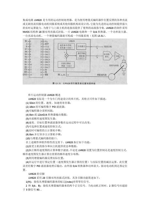
集成电路LM628是专用的运动控制处理器,是为使用增量式编码器作位置反馈的各种直流或无刷直流伺服电动机伺服系统或其他伺服机构而设计的,它能为先进的运动控制提供强大的实时运算能力。
为便于与上级主机的连接而提供了便利的高级指令集。
LM628的制作采用NMOS结构和28脚双列直插式封装,一片LM628电路和一个D/A转换器、一个功率放大器、一台直流电动机、一个增量编码器就可构成一个伺服系统(见图13.31)。
单片运动控制器LM628概述LM628实际是一个为专门用途设计的单片机,其特点可作如下描述:(1) 32bit的位置、速度、加速度寄存器;(2) 16bit的可编程数字PID滤波器;(3)可编程微分采样间隔;(4) 8bit或12bitD/A转换器输出数据;(5)内部梯形速度图发生器;(6)速度、目标位置和滤波器参数在运动过程中可以改变;(7)可选择位置或速度控制方式;(8)实时可编程的主计算机中断;(9) 8bit并行异步主计算机中断;(10)与增量式编码器的接口。
在上述硬件和软件特性的支持下,LM628执行如下功能:(1)接受主机的指令和向主机提供状态和数据;(2)执行梯形速度图的计算和数字滤波,不论是LM628设置为位置控制还是速度控制方式,梯形速度图发生器计算出需要的梯形速度分布图;(3)利用增量编码器反馈实际位置;(4)在运行中进行预定位置(速度图发生器计算的位置)与实际位置的减法运算,此位置误差经数字PID滤波器处理后输出,由外接D/A转换器和功率放大,驱动电动机到达预定位置。
LM628的引脚LM628采用28引脚双列直插式封装,其各引脚功能简述如下:1(IN):接收从增量编码器来的标记(index)亦即零位信号。
2和3(A、B):接收从增量编码器来的两个正交信号。
当电动机正转时,2脚信号应超前于3脚信号90。
4~11(DO~D7):连接主计算机或主处理器的I/O口。
利用CS(12脚)、PS(16脚)、RD (13脚)和WR(15脚)可向LM628写入指令和数据,或从LM628'读出状态字节和数据。
北京大华无线电仪器有限责任公司 2018产品目录说明书

2018PRODUCT CATALOG北京大华无线电仪器有限责任公司(简称:大华电子,原国营768厂),始建于1958年,2018年北京大华电子将迎来60岁华诞。
作为我国最早建成的微波测量仪器大型军工骨干企业,大华人以发展中国测量仪器工业为已任,专注于测试仪器行业,奋勇前行,不断创新。
目前产品已覆盖精密电子测量仪器、自动化测试系统、行业应用解决方案等数百种产品,并广泛应用于军工、科研、高校、通讯、工业控制、汽车电子、新能源等领域。
作为国产测量仪器行业的首创者和领航者,在过去60年间,大华人为客户提供了高质量产品和服务,同时,也为行业的培育、规范、发展做出了自己应有的贡献。
近年来,随着市场需求的不断升级和市场竞争的不断加剧,大华人持续创新,主动求变,引领和推进产业升级。
深入学习贯彻党的十九大精神,“不忘初心,牢记使命”,大华将传承多年的行业经验,通过研发平台升级,致力于高端测量仪器的开发和新行业的测试解决方案的拓展,为新老客户提供全方位的服务。
2018年,将是大华人新的起点,我们将深入持续创新,全面升级迎发展,继续与终端客户、合作伙伴紧密合作,加强军民融合和产学研深度融合,不断推进民用测试仪器的研制开发和高校研究成果的转化,进一步为工业市场提供更具稳定实用的仪器设备及解决方案,为国防建设、电子测量仪器事业的发展做出更大的贡献。
可靠性设计:简化、冗余设计并采用成熟技术方案,MTTF≥5000hrs。
维修性:采用单元模块化设计,便于拆卸、安装,对部件标准化设计,增加产品的互换性。
MTTR≦30min。
保障性:提供全套设备维修手册,并按需为使用及维修人员开展专业培训。
测试性:简化测试及调试设计,提高软件自检功能,提高测试效率。
安全性:确保无害输出,无易碎材质,产品在使用及损坏时不会造成人身伤害。
环境适应性:全部优选合格供应商产品,电子元器件筛选并降额使用。
交、直流分离设计,并采用有效材料增加电磁屏蔽效果。
器件厂商索引(分4页显示121条记录以厂商开头英文字母排序

atecom 专业生产 ATM 通信范畴的电路。
Atmel 美国爱特梅尔公司 AT 系列电路主要有:各类存储器、智能卡 IC、
Epson 专业生产打印机,但很多电子产品上有该公司的元器件、LCD.
EXAR 公司以生产数据通信领域中的电路为著称。
Fujitsu 产品以计算机周边电路、通信、工业类电路为主。
GEC Plessey Semiconductors GPS 半导体专业于广播、无线通信、雷达、
GSM 移动通信电路,品种规格较齐全,欧洲生产的电子产品大多采用该公司的器 件。
Avance Logic,Inc.计算机多媒体芯片组生产商,声霸卡芯片支持
Internet Phone。 AVX/Kyocera 产品范围较广,有电阻、电容、薄膜电路、表面安装元件、 滤波器、电压调整器、时基电路等等。 Benchmarq Microelectronics, Inc. 专业于电池充电监测控制、气体监测、 实时时钟等电路的生产。 Burr Brown CorporationBB 公司的各类转换电路、高精度模拟电路及各类 专用处理电路模块等等一直在国际上享有盛名。
American Microsystems 混合信号/数字 ASICs 专业厂商。
AMLogic,Inc. VCD/DVD MPEG-1 及 MPEG-2 视频/音频解码器制造商。
Amplifonix, Inc RF/Microwave 器件专业厂商。 Analog Devices ADI,美国模拟器件公司,国际上著名的高精度模拟电路 制造商之一, 生产有线性电路、混合信号电路、各类数据转换及放大处理电路等。
国内mems企业大全!
忽悠人的,没啥东西,建议不用下载了。
原文内容如下:MEMS公司企业和研究机构列表研究机构:东南大学MEMS教育部重点实验室2, 北京大学微电子学研究院和微米/纳米加工技术国家级重点实验室3, 北京国浩微磁电子智能传感器技术研究所, 北京海淀区, 电子科技集团第13所-国家'863'MEMS专项基地,,河北石家庄新华区合作路, 加速度传感器,陀螺仪,碰撞传感器,倾角传感器,振动传感器,流量传感器,光开关,光衰减器,光反射镜,RF开关,微波移相器,微波带通滤波器5, 中国电子科技集团公司第49所,哈尔滨南岗区一曼街,力/温/湿/气/磁/光6个方面,100多种传感器.20余年MEMS研究,服务国防及重点工程公司企业1. 华润半导体(香港)有限公司,香港,RF MEMS SWITCH,(为美国TERAVICTA代工),硅microphone)2. Memsic-美新半导体(无锡)有限公司,无锡,麦克风3. 楼氏声学公司(Knowles Acoustics),苏州,各类传感器4, 山东歌尔电子有限公司- 歌尔声学股份有限公司,潍坊总部,MEMS部在北京,硅microphone5, 北京青鸟元芯微系统科技有限公司,压力传感器,加速度传感器,湿度传感器6, 博世传感器公司(Bosch Sensortec),医疗(加速度计--药物释放/生物分析,步数计),消费(笔记本坠落感测,振动感测,3D游戏杆),安全工程7, ST-意法半导体8, ADI29, 摩托罗拉10, HP-惠普,喷墨打印机头`11. 英飞凌,TPMS用MEMS传感器,已经与IC完美集成!很厉害!12. 苏州敏芯微电子技术有限公司,硅基MEMS麦克风(07年11月发布,08年批量还有其它的,例如上海巨哥电子科技有限公司,深圳市卡默莱电子科技有限公司,烟台睿创微纳技术有限公司Raytron,上海三鑫科技发展有限公司(Laseno微型激光投影仪)目前,国内MEMS产品门类依然相对较少,主要还是以惯性器件和压力传感器为主,而且多是中低端产品,创新性强的新器件、新系统鲜有出现高校和研究所:北京大学、1000m2 MEMS 洁净室中科院上海微系统与信息技术研究所,1600m2MEMS 洁净室河北半导体研究所(13所)1000m2MEMS 洁净室厦门大学萨本栋微纳米技术研究中心600m2洁净室中国工程物理研究院微系统中心1000 m2洁净室中国科学院微电子研究所中国科学院苏州纳米技术与纳米仿生研究所北京国浩微磁电子智能传感器技术研究所其它的诸如:山东淄博国家高新区MEMS研究院、陕西省微型机械电子系统研究中心、西安212/213所、618所,航天717/704所等等,大连理工王立鼎院士的分析是:研发的分布地区和单位:中国内地MEMS的研发单位主要集中在华北、华东和东北三个地区,还有西南地区的重庆和西北地区的西安等。
ARMCortex-M系列的微控制器半导体厂商
半导体厂商名单爱特梅尔公司(Atmel Corporation)Mentor Graphics公司恩智浦东芝意法半导体(ST)MATHWORKS富士通半导体德州仪器(TI)飞思卡尔半导体赛普拉斯半导体公司(Cypress)SparkFun 公司Silicon Image(矽映电子科技)Infineon英飞凌Embedded ArtistsNuvoton新塘科技)红熊电子亚德诺半导体(ADI)北京兆易创新深圳市英培特有限公司(Embest)韩国WIZnet公司Netduino一恩智浦(NXP)1,LPC824Lite采用NXP LPC28x系列微控制器LPC824,运行频率高达30MHz,是LPC800系列中最新推出的一款产品。
特点:基于ARM Cortex-M0+内核,在LPC81x的基础上新增加了高速高精度模拟-数字转换模块、更丰富的串行接口设备、更大的程序存储空间。
应用:适用于马达控制、智能家电、工业自动化等多个领域。
2,LPCXpresso™是由恩智浦提供的一个低成本开发平台,它支持恩智浦基于ARM Cortex-M4的微控制器。
特点:该平台包括一个基于Eclipse的简化IDE和附带JTAG调试器的低成本目标板。
LPCXpresso 是一个端到端解决方案,支持嵌入式工程师开发从初始评估到最终生产的所有应用程序。
应用:用于支持LPC112x系列MCU的评估和原型设计3,LPC824 Cortex-M0+微控制器的LPCXpresso824-MAX 开发板被设计用于让客户尽可能容易地启动项目。
特点:LPCXpresso824-MAX 包含一个标准的10 引脚JTAG/SWD 连接器以及若干模拟/数字扩展头,使其成为高度可扩展的平台。
符合LPCXpresso™、Arduino UNO 和PMOD 标准扩展头,给想利用现有外接电路板的开发者提供了前所未有的多样化选择应用:LPCXpresso824-MAX 经配置,可使用来自Keil、IAR 的外部调试探测器,以及支持CMSIS-DAP 的其他开发工具。
LM628
TRI-STATE is a registered trademark of National Semiconductor Corporation
TL H 9219 – 1
FIGURE 1 Typical System Block Diagram
Connection Diagrams
LM628N LM629N LM629M
C1995 National Semiconductor Corporation TL H 9219 RRD-B30M115 Printed in U S A
Absolute Maximum Ratings (Note 1)
If Military Aerospace specified devices are required please contact the National Semiconductor Sales Office Distributors for availability and specifications Voltage at Any Pin with Respect to GND Ambient Storage Temperature Lead Temperature 28-pin Dual In-Line Package (Soldering 4 sec ) 24-pin Surface Mount Package (Soldering 10 sec )
AC Electrical Characteristics
(VDD and TA per Operating Ratings fCLK e 6 MHz CLOAD e 50 pF Input Test Signal tr e tf e 10 ns) Timing Interval ENCODER AND INDEX TIMING (See Figure 2 ) Motor-Phase Pulse Width Dwell-Time per State Index Pulse Setup and Hold (Relative to A and B Low) CLOCK AND RESET TIMING (See Figure 3 ) Clock Pulse Width LM628N-6 LM629N-6 LM629M-6 LM628N-8 LM629N-8 LM629M-8 Clock Period LM628N-6 LM629N-6 LM629M-6 LM628N-8 LM629N-8 LM629M-8 Reset Pulse Width T4 T4 T5 T5 T6 78 57 166 125 8 fCLK ns ns ns ns ms T1 T2 16 fCLK 8 fCLK 0 ms ms ms T Min Tested Limits Max Units
infineon TLE6282G Dual Half Bridge Driver IC 说明书
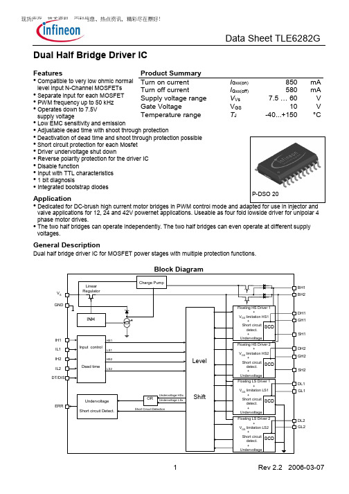
现货库存、技术资料、百科信息、热点资讯,精彩尽在鼎好!Data Sheet TLE6282GDual Half Bridge Driver ICFeatures• Compatible to very low ohmic normal level input N-Channel MOSFETs • Separate input for each MOSFET• PWM frequency up to 50 kHz• Operates down to 7.5Vsupply voltage • Low EMC sensitivity and emission• Adjustable dead time with shoot through protection• Deactivation of dead time and shoot through protection possible • Short circuit protection for each Mosfet • Driver undervoltage shut down• Reverse polarity protection for the driver IC • Disable function• Input with TTL characteristics • 1 bit diagnosis• Integrated bootstrap diodesApplication•Dedicated for DC-brush high current motor bridges in PWM control mode and adapted for use in injector and valve applications for 12, 24 and 42V powernet applications. Useable as four fold lowside driver for unipolar 4 phase motor drives.• The two half bridges can operate independently. The two half bridges can even operate at different supply voltages.General DescriptionDual half bridge driver IC for MOSFET power stages with multiple protection functions.Input controlDead time UndervoltageShort circuit Detect.ORINHCharge PumpLevelShiftFloating LS Driver 1+V GS limitation LS1+Short circuitdetect.+Undervoltage Linear RegulatorUndervoltage HSx Undervoltage LSxHS1LS2HS2LS1V S GNDIH2ERRBH1BH2SH1GH1DH1GH2DH2GL1SH2GL2DL1DL2Floating LS Driver 2+V GS limitation LS2+Short circuitdetect.+UndervoltageFloating HS Driver 2+V GS limitation HS2+Short circuitdetect.+Undervoltage Floating HS Driver 1+V GS limitation HS1+Short circuitdetect.+Undervoltage SCD SCD SCD SCD Short Circuit DetectionIL2IH1IL1Product SummaryTurn on current I Gxx(on) 850 mA Turn off current I Gxx(off) 580 mA Supply voltage range V Vs 7.5 … 60 VGate Voltage V GS 10 V Temperature range T J -40...+150 °CP-DSO 20SH1TLE 4278GV S =12VC S 47µFC D 47nFD IQResetW atchdogC Q 22µFµCGH1R Q 47 k ΩDH1BH1SH2GH2DH2BH2GL1DL1GNDGL2DL2VS W D RV CCER1DT/DISR Q 47 k ΩIH1IL1IH2IL2Load 2Load 1C B220nFC B220nFC S 1µFR 10 ΩThis application diagram shows the principle schematics of a typical injector / valve drive. Other configurations are possible as well. Freewheeling diodes are not considered. The 10 m Ω resistor is not needed by the Driver IC, but may be needed for load current measurement. The voltage devider networks, e.g. R = 10 k Ω, across the two Low Side MOSFETs are an example as well; they allow to increas the current limit threshold for Short Circuit protection SCD for the Low Side MOSFETs. As they pull down the Sources of the High Side MOSFETs (while the Low Side MOS-FETs are off), they allow to pre-charge the C Bx capacitors during start-up (before the Driver IC gets enabled). The SCD current limit threshold can be increased for the High Side MOSFETs as well by using voltage devider networks across the High Side MOSFETs. SCD can also be dis-abled (High Side and / or Low Side MOSFETs).Pin Symbol Function 1DT/DISa) Set adjustable dead time by external resistor b) Deactivate deadtime and shoot through protectionby connecting to 0V c) Reset ERR register d) Disable output stages2 ERR Error flag for driver shut down3 IH1 Control input for high side switch 14 IL1 Control input for low side switch 15 IH2 Control input for high side switch 2 6IL2Control input for low side switch 17 GND Ground 8 VS Voltage supply 9 DL2 Sense contact for short circuit detection low side 2 10 DL1 Sense contact for short circuit detection low side 1 11 GL1 Output to gate low side switch 1 12 SH1 Connection to source high side switch 1 13 GH1 Output to gate high side switch 1 14 BH1 Bootstrap supply high side switch 115 DH1 Sense contacts for short circuit detection high side 1 16 DH2 Sense contacts for short circuit detection high side 2 17 BH2 Bootstrap supply high side switch 2 18 GH2 Output to gate high side switch 2 19 SH2 Connection to source high side switch 2 20GL2Output to gate low side switch 21112131415161718192010DT/DIS GL1SH1 GH1 DL2 VS BH1 GND DH1 IL2 DH2 BH2 IH2 IL1 GH2 SH2 GL2 IH1 ERR DL1TLE6282G198********Maximum Ratings at T j =-40…+150°C unless specified otherwiseParameter Symbol Limits Values Unit Supply voltage 1 V S -4 60V Operating temperature range Storage temperature range T j T stg-40 -55 150150°CMax. voltage range at Ixx; DT/DIS -1 6V Max. voltage range at ERR -0.3 6V Max. voltage range at BHx V BHx -0.3 90V Max. voltage range at DHx 2 V DHx -4 75V Max. voltage range at GHx 3 V GHx -7 86V Max. voltage range at SHx 3 V SHx -7 75V Max. voltage range at DLx V DLx -7 75V Max. voltage range at GLx V GLx -2 12V Max. voltage difference BHx - SHx V BHx -V SHx -0.3 17V Max. voltage difference GHx – SHx; GLx V Gxx -V Sxx -0.3 11V Power dissipation (DC) @ T A =125°C / min.footprint P tot 0.33W Power dissipation (DC) @ T A =85°C / min.footprint P tot 0.85WElectrostatic discharge voltage (Human Body Model) according to MIL STD 883D, method 3015.7 and EOS/ESD assn. standard S5.1 – 1993 V ESD 42kV Jedec Level 3Thermal resistance junction - ambient (minimal foot-print with thermal vias)R thJA 75K/W Thermal resistance junction - ambient (6 cm 2)R thJA75K/WFunctional rangeParameter and Conditions Symbol Values Unit at T j = –40…+150 °C, unless otherwise specifiedSupply voltageV S 7.5 60V Operating temperature rangeT j -40 150°C Max. voltage range at Ixx, DT/DIS -0.3 5.5V Max. voltage range at ERR -0.3 5.5V Max. voltage range at BHx V BHx -0.3 90V Max. voltage range at DHx 2 V DHx -4 75V Max. voltage range at GHx 3 V GHx -7 86V Max. voltage range at SHx 3V SHx -7 75V1With external resistor (≥10 Ω ) and capacitor 2The min value -4V is increased to –( V BHx - V SHx ) in case of bootstrap voltages <4V 3The min value -7V is reduced to –(V BHx -V SHx -1V) in case of bootstrap voltages <8V 4All test involving Gxx pins V ESD =1 kV!Max. voltage range at DLx3 V DLx-7 75 VMax. voltage range at GLx V GLx-2 12VMax. voltage difference BHx - SHx V BHx-V SHx-0.3 12VMax. voltage difference GHx – SHx; GLx V Gxx-V Sxx-0.3 11VPWM frequency F PWM0 50kHzt p(min)2µsMinimum on time external lowside switch – static con-dition @ 20 kHz; Q Gate = 200nCElectrical CharacteristicsUnitValues Parameter and Conditions Symbolat T j = –40…+150 °C, unless otherwise specifiedmin typ maxand supply voltage range V S = 7.5 ... 60V; f PWM = 20kHzStatic CharacteristicsLow level output voltage (V GSxx) @ I=10mA ∆V LL-- 60 150mV∆V HL8 10 11VHigh level output voltage (V GSxx) @ I=-10mA;Vs>12VSupply current at VS(device disabled)I VS(dis)14V-- 4 8mA@ V bat= V S =14V R DT=400kΩSupply current at VS(device disabled)I VS(dis)42V-- 4 8mA@ V bat= V S =42V R DT=400kΩI VS(open)14V-- 7 15mASupply current at V S@ V bat= V S =14V 20kHz (Out-puts open)Supply current at V S@ V bat= V S =14V 50kHz (Out-I VS(open)14V-- 7 15mAputs open)I VS(open)42V-- 7 15mASupply current at V S@ V bat= V S =42V 20kHz (Out-puts open)Low level input voltage V IN(LL) --1.0V--High level input voltage V IN(HL) 2.0 -- --VInput hysteresis ∆V IN100 170 mVDynamic characteristics (pls. see test circuit and timing diagram)Turn on current @ V Gxx -V Sxx = 0V; T j=25°C @ V Gxx -V Sxx = 4V; T j=125°C @ C Load=22nF; R Load=0ΩI Gxx(on) ----850700----mATurn off current @ V Gxx -V Sxx = 10V; T j=25°C @ V Gxx -V Sxx = 4V; T j=125°C @ C Load=22nF; R Load=0ΩI Gxx(off) ----580300----mADead time (adjustable) @ R DT = 1 kΩ@ R DT = 10 kΩ @ R DT = 50 kΩ @ R DT = 200 kΩ @ C Load=10nF ; R load=1Ωt DT --0.050.40--0.241.03.1--0.382.50--µsRise time @ C Load=10nF ; R load=1Ω (20% to 80%) t rise-- 100 300ns Fall time @ C Load=10nF ; R load=1Ω (80% to 20%) t fall-- 150 440ns Disable propagation time@ C Load=10nF ; R load=1Ωt P(DIS) 3.4 5 7µsReset time of diagnosis@ C Load=10nF ; R load=1Ωt P(CL) 1 2 3.1µsInput propagation time(low side turns on, 0% to 10%)t P(ILN)-- 160 500nsInput propagation time(low side turns off, 100% to 90%)t P(ILF)-- 100 500nsInput propagation time(high side turns on, 0% to 10%)t P(IHN)-- 120 500nsInput propagation time(high side turns off, 100% to 90%)t P(IHF)-- 120 500nsInput propagation time difference(all channels turn on)t P(Diff)20 40 70nsInput propagation time difference(all channels turn off)t P(Diff)-- 20 50nsInput propagation time difference (one channel; low on – high off) t P(Diff) --40150nsInput propagation time difference (one channel; high on – low off) t P(Diff) --20150nsInput propagation time difference (all channels; low on – high off) t P(Diff) --40150nsInput propagation time difference (all channels; high on – low off) t P(Diff) --20150nsTest Circuit and Timing DiagramDiagnosis and Protection Functions Short circuit protection filter time t SCP(off) 69 12µs Short circuit criteria (V DS of Mosfets) For Low Sides For High Sides V DS(SCP) 0.5 0.450.75 0.75 1.01.05V Disable input levelV DIS 3.3 3.7 4.0V Disable input hysteresis∆V DIS 180 mV Deactivation level for dead time and shoot through protectionV DIS 0.6 0.85 1.1V Deactivation input hysteresis ∆V DIS 170 mV *****************ERRV ERR -- -- 1.0V Under voltage lock out for highside output – boot-strap voltageV BHx (uvlo) 3.7 4.6V Under voltage lock out for lowside output – supply voltageV Vs (uvlo)4.85.9VTest Conditions :Junction temperature T j = -40 … 150o C Supply voltage range Vs = 7.5 … 60V PWM frequency f PWM = 20 kHzGHxGLxSHxx2V GHX_C R load = 1 Ohm load= 10 nF I HXR load = 1 Ohm load= 10 nF V GLX_C I LXtttIHx+ ILx50%20%80%20%80%tttttttt10%90%90%10%GHX_CV GLX_CVRemarks:Default status of input pins:To assure a defined status of all input pins in case of disconnection, these pins are internally secured by pull up / pull down current sources with approx. 20µA. The following table shows the default status of each input pin.Input pin Default status ILx (active high) Low IHx (active low) High DT/DIS (active high) HighDefinition:In this datasheet a duty cycle of 98% means that the GLx pin is 2% of the PWM period in high condition.Functional descriptionDescription of Dead Time Pin / Disable Pin / ResetIn the range between 1.5 and 3.5 V the dead time is varied from 100ns to 3.1µs typ. In the range below 1.0V the dead time is disabled / shoot through is allowed. Both external Mosfets of the same half bridge can be switched on simultaneously. This function allows the use of a half bridge for valves and injectors. In the range above 4.0V the device is disabled.If DIS is pulled up to 5V for 3.1 to 3.4µs only the ERR register is cleared (reset), no output stage is shut down. A shut down of all external Mosfets occurs if DIS is pulled up for longer than 7µs.Condition of DT/DIS pin Function 0 - 1V Disable of dead time; Shoot through is allowed 1.5 - 3.5V Adjust dead time between 100ns and 3.1µs typ. a) Reset of diagnosis register if DT/DIS voltage is higher than4V for a time between 3.1µs and 3.4µs> 4V b) Shut down of output stages if DT/DIS voltage is higher than 4V for a time above 7µs (Active pull down of gate volt-age)Description of DiagnosisThe ERR pin is an open collector output and has to be pulled up with external pull up resis-tors to 5V. In normal conditions the ERR signal is high. In case of shutdown of any output stage the ERR is pulled down. This shut down can be caused by undervoltage or short cir-cuit.Recommended Start-up procedureThe following procedure is recommended whenever the Driver IC is powered up:• Disable the Driver IC via DT/DIS pin• After the supply voltage has ramped up, wait for several ms to pre-charge the boot-strap capacitors of the High Side MOSFETs C Bx through the resistors R on the DLxpins (voltage devider network, pls. see Application block diagram on pg. 2) t WAIT≈ 3 x C Bx x 2 x R, whereas R = 10 kΩ•Enable the Driver IC via DT/DIS pin•Start the operation by applying the desired pulse patterns. Do not apply any pulse pat-terns to the IHx or ILx pins, before the C Bx capacitors are charged up.Alternatively, the Driver IC can be enabled via the DT/DIS pin right after ramping up the sup-ply voltage V S. Now, the two Low Side MOSFETs are turned on via the ILx control inputs (topull down the Sources of the High Side MOSFETs and to charge up the bootstrap capacitorsC Bx within several 10 µs). The regular operation can be started when the bootstrap capaci-tors are charged up.Short Circuit protectionThe current threshold limit to activate the Short Circuit protection function can be adjusted to larger values, it can not be adjusted to lower values. This can be done by external resistorsto form voltage deviders across the “sense element” (pls. see Application block diagram onpg. 2), consisting of the Drain-Source-Terminals, a fraction of the PCB trace and – in some cases – current sense resistors (used by the µC not by the Driver IC).The Short Circuit protection can be disabled for the High Side MOSFETs by shorting DH1with SH1 and DH2 with SH2 on the PCB; in this case the DHx pins may not be connected tothe Drains of the associated MOSFETs. To disable Short Circuit protection for the Low Side MOSFETs the DL1 and DL2 pin should be connected to the Driver IC´s Ground.Shut down of the driverA shut down can be caused by undervoltage or short circuit.A short circuit will shut down only the affected Mosfet until a reset of the error register by a disable of the driver occurs. A shut down due to short circuit will occur only when the Short Circuit criteria V DS(SCP) is met for a duration equal to or longer than the Short Circuit filter timet SCP(off). Yet, the exposure to or above V DS(SCP) is not counted or accumulated. Hence, repeti-tive Short Circuit conditions shorter than t scp(off) will not result in a shut down of the affected MOSFET.An undervoltage shut down shuts only the affected output down. The affected output willauto restart after the undervoltage situation is over.Operation at Vs<12VIf Vs<11.5V the gate voltage will not reach 10V. It will reach approx. Vs-1.5V, dependent onduty cycle, total gate charge and switching frequency.Operation at different voltages for Vs, DH1 and DH2If DH1 and DH2 are used with a voltage higher than Vs, a duty cycle of 100% can not be guaranteed. In this case the driver is acting like a normal driver IC based on the bootstrap principle. This means that after a maximum “On” time of the highside switch of more than1ms a refresh pulse to charge the bootstrap capacitor of about 1µs is needed to avoid un-dervoltage lock out of this output stage.Operation at extreme duty cycle:The integrated charge pump allows an operation at 100% duty cycle. The charge pump is strong enough to replace leakage currents during “on”-phase of the highside switch. Thegate charge for fast switching of the highside switches is supplied by the bootstrap capaci-tors. This means, that the bootstrap capacitor needs a minimum charging time of about 1µs,if the highside switch is operated in PWM mode (e.g. with 20kHz a maximum duty cycle of96% can be reached). The exact value for the upper limit is given by the RC time formed bythe impedance of the internal bootstrap diode and the capacitor formed by the external Mos-fet (C Mosfet =Q Gate / V GS ). The size of the bootstrap capacitor has to be adapted to the external MOSFET the driver IC has to drive. Usually the bootstrap capacitor is about 10-20 times big-ger then C Mosfet . External components at the Vs Pin have to be considered, too.General remark:It is assured that after the removal of any fault condition, which did not damage the device, the device will return to normal conditions without external trigger. Only short circuit condition needs restart by reset.Estimation of power loss within the Driver ICThe power loss within the Driver IC is strongly dependent on the use of the driver and the external components. Nevertheless a rough estimation of the worst case power loss is pos-sible.Worst case calculation is:P Loss = (Q gate *n*const* f PWM + I VS(open)/20kHz)* V Vs - P RGate With:P Loss = Power loss within the Driver IC f PWM = Switching freqencyQ gate = Total gate charge of used MOSFETs at 10V V GS n = Number of switched MOSFETsconst = Constant considering some leakage current in the driver (about 1.2)I VS(open) = Current consumption of driver without connected Mosfets during switching V VS = Voltage at VsP RGate = Power dissipation in the external gate resistorsThis value can be reduced dramatically by usage of external gate resistors.Conditions :Junction temperature T j = 25o CNumber of switched MOSFET n = 2Power dissipation in the external gate resistors P RGate = 0,2*P LossEstimated Power Loss P LOSS within the Driver ICfor different supply voltages V sat Q G = 100nC @ V GS = 10V00,10,20,30,40,50,60,70,80102030405060PWM Frequency (kHz)P L O S S (W )Vs = 8VVs = 14V Vs = 18VEstimated Power Loss P LOSS within the Driver ICfor different gate charges Q G at supply voltage V s = 14V00,10,20,30,40,50,60,70,80102030405060PWM Frequency (kHz)P L O S S (W )Q G = 50nC Q G = 100nC Q G = 200nCBHxGHxi Gxx(on)i Gxx(on)i Gxx(off)i Gxx(off)V IHxi GHxi GHx850 mA Peak580 mA PeakTest Conditions :- Turn On : V GS = 0V, T j = 25o C - Turn Off : V GS = 10V, T j = 25o CThis figure represents the simplified internal circuit of one high side gate drive. The drive circuit of the low sides looks similar.LoadV sTLE6282G High Side DriverThis figure illustrates typical voltage andcurrent waveforms of the high side gate drive;the associated waveforms of the low side drives look similar.Logic + Level Shift + V GS limit +Under voltageV IHxC BDHx SCDSHxGate Drive characteristicsTruth TableInput Conditions OutputILx IHx DT / DIS UV SC GLx GHx ERR1 1<3.5V 0 0 1 0 5V 0 0 <3.5V 0 0 0 1 5V 1 0 1.5-3.5V 0 0 A A 5V 1 0 <1V 0 0 1 1 5V 01 <3.5V0 05V1 1 <3.5V 10 B 0 C 0 0 <3.5V 1 0 0 B C 1 0 1.5-3.5V 1 0 D D C 1 0 <1V 1 0 B B C 01 <3.5V1 0C1 1 <3.5V 01 E 0 F 0 0 <3.5V 0 1 0 E F 1 0 1.5-3.5V 0 1 D D F 1 0 <1V 0 1 E E F 01 <3.5V0 1FX X X X X 0 0 5V X X >4V X X 0 0 5VA) stays in the condition before the shoot throught command occurs (see also dead time diagrams)B) 0 when affected; 1 when not affected; self recoveryC) 0V when output does not correspond to input patterns; 5V when output corresponds to input patterns.D) stays in the condition before the shoot throught command occurs (see also dead time diagrams); 0 when affectedE) 0 when affected– the outputs of the affected halfbridge are shut down and stay latched until reset; 1 when not affectedF) 0V when output does not correspond to input patterns – the outputs of the affected half-bridge are shut down and stay latched until reset; 5V when output corresponds to input patterns.X) Condition has no influenceRemark: Please consider the influence of the dead time for your input duty cyclePackage and Ordering Code (all dimensions in mm)Package CodeP-DSO 20Published byInfineon Technologies AG,Bereich KommunikationSt.-Martin-Strasse 53,D-81541 München© Infineon Technologies AG 1999All Rights Reserved.Attention please!The information herein is given to describe certain components and shall not be considered as warranted char-acteristics.Terms of delivery and rights to technical change reserved.We hereby disclaim any and all warranties, including but not limited to warranties of non-infringement, regarding circuits, descriptions and charts stated herein.Infineon Technologies is an approved CECC manufacturer.InformationFor further information on technology, delivery terms and conditions and prices please contact your nearest In-fineon Technologies Office in Germany or our Infineon Technologies Representatives worldwide (see address list).WarningsDue to technical requirements components may contain dangerous substances. For information on the types in question please contact your nearest Infineon Technologies Office.Infineon Technologies Components may only be used in life-support devices or systems with the express written approval of Infineon Technologies, if a failure of such components can reasonably be expected to cause the fail-ure of that life-support device or system, or to affect the safety or effectiveness of that device or system. Life support devices or systems are intended to be implanted in the human body, or to support and/or maintain and sustain and/or protect human life. If they fail, it is reasonable to assume that the health of the user or other per-sons may be endangered.。
中国十大芯片制造厂精度
中国十大芯片制造厂精度中国芯片制造行业正迅速崛起,已经成为全球领先的芯片制造国家之一。
正是凭借着高精度的制造工艺和先进的技术,中国的芯片厂商在国际市场上取得了巨大的成功。
本文将介绍中国十大芯片制造厂的精度技术。
1. 中芯国际(SMIC)中芯国际是中国最大的芯片制造企业之一,其在工艺技术方面取得了显著的突破。
公司通过自主研发和技术引进,实现了7纳米工艺的大规模生产,使得芯片的制造精度达到了国际水平。
2. 科达利(Hua Hong)科达利是中国主要的集成电路制造企业之一,其在工艺精度方面表现出色。
通过持续的技术创新和改进,科达利成功地制造出了高精度、高集成度的芯片产品,在国内外市场上受到广泛认可。
3. 华力微电子(HL Micro)华力微电子是中国芯片制造行业的领导者之一,其在精度控制方面经验丰富。
公司拥有世界一流的制造设备和技术团队,能够精确控制每个制造步骤,确保芯片的高精度和可靠性。
4. 联华电子(Unisoc)联华电子是中国芯片制造的知名企业,其在制造工艺精度方面具有先进的技术和经验。
公司致力于研发和生产高质量的芯片产品,通过不断改进工艺控制和质量管理,实现了较高的精度水平。
5. 全志科技(Allwinner)全志科技是中国知名的芯片制造企业,其在工艺精度方面具备显著的竞争优势。
公司通过技术创新和优化,成功地制造出多款高性能、高精度的芯片产品,赢得了广大客户的赞誉。
6. 瑞芯微(Rockchip)瑞芯微是中国领先的芯片设计和制造公司之一,其在工艺精度方面拥有深厚的专业知识。
公司通过严格的制造流程和高精度的设备,使得其芯片产品具有出色的精度和稳定性。
7. 中天微(RDA Microelectronics)中天微是中国专业的无线通信芯片制造企业,其在精度控制方面具备专业的技术知识。
公司通过优化制造工艺和质量管理,不断提高芯片的制造精度和可靠性,为客户提供高品质的芯片产品。
8. 晶方科技(Jingfang Technology)晶方科技是中国集成电路制造行业的佼佼者之一,其在工艺精度控制方面具有独到的优势。
LM1893工作原理

LM1893工作原理以通用电力线载波通讯芯片LM1893为核心,以AT89C51单片机为主控单元,建立一个点对点的电力线载波通信系统,在电力线上实现数据电力线载波通信是利用现有的电力线路来传输信号的,其工作原理简述为:将数据或语音调制在几十至几百KHz的载波频率上通过电力线发送出去,接收端将电力线上载有信号的载波接收下来进行解调还原出原来的语音或数据。
通信的载体即现成的电力线,无需象有线通信一样重新铺设通信线路。
也不象无线传输那样需要复杂的发送接收设备来传输信息。
它无需架设额外的通信线路,也不占用宝贵的无线频谱资源,因此很适合于小集团内部(一般在同一个电力变压器间)组成局域网络达到数据或语音的传输目的。
LM1893是美国国家半导体器件公司(National Semiconductor)开发的电力线载波通信集成电路,集成了发送和接收数据的全部功能,可实现串行数据的半双工通信。
只需少量的外接元件即可构成完整的电力线载波通信系统,适合于工业自动控制系统,楼宇数据或语音通信、家用电器集中控制、医院的紧急呼叫系统、防火报警及计算机数据传输等应用场合。
其主要功能特性如下:FSK抗噪声调制技术可选择噪声滤波的脉冲发生器数据传输率达4.8kB正弦波载频以降低射频干扰射频功率可增强10倍载波频率可在50—300kHz之间选择兼容TTL和MOS逻辑电平可调节电压至功率电平可驱动现有的各种电力线路LM1893工作原理LM1893内部集成了发送和接收两个独立的部分,发送部分内置了FSK调制器、正弦波发生器、电流型控制振荡器、自动增益控制电路(ALC)及输出功率放大器等单元电路。
接收部分包含了限幅放大器、锁相环解调器、低通滤波器、直流嵌位电路和噪声滤波器等单元电路。
TX/RX 为发送或接收的控制引脚,当TX/RX为高电平时,电路处于发送工作模式,数据信号从P17输入FSK调制器,形成开关控制电流并驱动振荡器产生±2.2%频偏的三角波,经正弦波整形电路输出正弦波信号,再经功率放大后由耦合线圈传输到电力线路上去。
HM6282内置MOS升压型大功率LED恒流驱动器典型应用电路图

参数 输入电压 芯片电源电压 系统工作频率
符号 VIN VDD FOP
最小值
典型值
最大值 50
单位 V V KHz
4.5
6.8
7 1000
3 of 5
HM6282 内置 MOS 升压型大功率 LED 恒流驱动器
调光频率 FPWM 250 1000 Hz
注 2:推荐工作范围是指在该范围内,器件功能正常,但并不完全保证满足个别性能指标。
5 of 5
HM6282 内置 MOS 升压型大功率 LED 恒流驱动器
封装信息
SOP14 封装参数
6 of 5
EN 使能端输入
EN 端输入高电平 EN 端输入低电平 大于 1.1V 无效 0.9 1.0 1.1 0.2 V V
低电平有效
典型升压豪华型应用电路(可设定恒流和恒压输出。带输入欠压保护功能和空载保护)
图 1:VIN=12~24VDC VOUT=38V.IOUT=0.65A 典型升压
经济型应用电路图 3(恒流精度为±3%.空载保护)
温度保护
温度 130 PC
o
短路保护
工作电流 IN:12VDC 0.8 mA
内置功率 MOS 管
最大漏源电压 导通内阻 MOS 管导通阈值 VDS_MAX RDS(ON) VTH VGS=4.5V , ID=8A 1 60 48 2.5 V mΩ V
4 of 5
HM6282 内置 MOS 升压型大功率 LED 恒流驱动器
电气特性 除非特别说明,VDD=5.6V,TA=25oC
参数
符号
测试条件 电源电压
最小值
典型值
最大值
单位
最大输入电压 欠压保护电压
+微控制器的电气接口
8
➢ 隔离接口
使两个子系统在电气上相互隔离,但仍可以通过光路来传递数 字信息,也称为光电隔离。可不需要共地连接,但反应慢。
➢ 串行接口
● 异步串行接口——双线接口, 一根发数据, 另一根接收数据,速 度较慢。有RS232和TTL两种逻辑电平方式。
● I2C接口——双线接口, 一根I/O线为时钟信号线发数据, 另一根 I/O线为数据传输线,速度稍快。
第六章 微控制器的电器接口
机器人控制器与电机驱动器的电气连接合理性和正确性, 是实现机器人可靠工作的重要保障。
6.1 机器人的微控制器
6.1.1 BS2 微控制器简介
➢ 常用的机器人控制电路和程序开发平台
● PC机的并口 ● Parallax公司的BASIC Stamp ● BasicX 公司的微控制器 ● OOpic 微控制器 ● National Semiconductor 公司的LM629运动控制器
● SPI接口——三线接口,串行时钟、中级
光电隔离
串行接口
9
6.2.2 与电源接口
10
主要参考文献: (1) [美] 丹尼斯. 克拉克等著,宗光华等译,机器人设计与控制,科学出版社,
2004.5. (2) 王华 等,电机专用运动控制器LM629 的应用研究,电子器件,2005,
28(2):370-373
系数由主处理器提供。
7
6.2 微控制器、计算机的电气接口
6.2.1 输入/输出接口 微控制器与驱动器及计算机或主处理器的接口有三种标
准方式可以采用:缓冲接口、隔离接口、串行接口。 ➢ 缓冲接口
● 电阻(无源)缓冲 ——与其它接口芯片间 ● 集成芯片(有源)缓冲——PC机与电路间的接口形式
- 1、下载文档前请自行甄别文档内容的完整性,平台不提供额外的编辑、内容补充、找答案等附加服务。
- 2、"仅部分预览"的文档,不可在线预览部分如存在完整性等问题,可反馈申请退款(可完整预览的文档不适用该条件!)。
- 3、如文档侵犯您的权益,请联系客服反馈,我们会尽快为您处理(人工客服工作时间:9:00-18:30)。
极限参数(Note1) 如果有军事/航天的设备的规定需求, 请联系国家半导体公司的销售\批发机构来取得产品和 详尽说明。 所有针脚对地电压 -0.3V~+7.0V 存储温度 -65~+150 焊接温度 28 针双列直插 4 秒 260 24 针贴片 10 秒 300 最大功耗 650mW(TA<85) (Note2) 抗静电 2000V(CZAP=120pF,RZAP=1.5k) 操作范围 温度范围 -40<Ta<+85 时钟频率 LM628N-6,LM629N-6,LM629M-6 1.0M<fCLK<6.0MHz LM628N-8,LM629N-8,LM629M-8 1.0M<fCLK<8.0MHz 4.5V<VDD<5.5V 电源电压 VDD 直流电气规格 (VDD 和 TA 符合操作范围,FCLK=6MHz) 符号 IDD 输入电压 VIH VIL IIN 逻辑 1 电平 逻辑 0 电平 输入电流 0≤VIN≤VDD IOH=-1.6mA IOL=1.6mA 0≤VOUT≤VDD -10 -10 2.4 0.4 10 2.0 0.8 10 V V uA V V uA 定义 条件 测试的极限 最小 供应电流 开路输出 110 最大 mA 单位
引脚 16(9) ,端口选择(/PS)输入:用于选择指令或者数据端口。低电平选择指令,高电 平选择数据。以下模式由引脚 16 控制: 1.向端口写入指令(低电平) 。 2.状态字从端口读出(低电平) ,以及(译注:原文缺失) 3.通过端口读写数据(高电平) 。 引脚 17(10) ,主机中断(HI)输出:这个高有效的信号通过主机中断服务警告主机有中断 发生。 引脚 18~25,DAC 端口(DAC0~DAC7) :用在三种不同模式下的输出端口。 1.LM628(8 位输出模式) :向 DAC 输出所存的数据。高位在 18 脚,低位在 25 脚。 2.LM628(12 位数触摸式) :分开输出两个 6 位字。低位字先输出。高位在 18 脚,低位在 23 脚,24 脚用于分辨他们。25 脚信号的上升沿用于所存输出的数据。Figure 8 显示了多元 信号的时间关系。 3.LM629(符号\量值 输出模式) :在 18 脚(贴片的 11 脚)输出一个 PWM 符号信号,并在 19 脚 (贴片的 13 脚) 输出一个 PWM 的量值信号。 在 LM629 里引脚 20~25 没有使用。 Figure 11 显示了 PWM 输出信号格式。 引脚 26(14) ,时钟(CLK)输入:接收系统时钟。 引脚 27(15) ,复位(/RST)输入:低电平有效,上升沿触发,复位以下列出的 LM628 内部 状态。注意复位脉冲必须逻辑低并且超过 8 个时钟周期。以下为复位所作的。 --------------------------------------------------------------------------------------------------------------------------------1.滤波器系数和轨迹参数置零。 2.设置位置误差门槛最大值(7FFFH) ,并且切实运行指令 LPEI。 3.屏蔽了 SBPA/SBPR 中断(禁止) 。 4.开放 5 个其它中断(使能) 。 5.初始化当前位置为 0 或者“终点”位置。 6.设置微分采样间隔为 2048/fCLK 或者是用 8.0MHz 时钟的 256us。 7.DAC 端口输出一个 12 位 DAC 的零点 800H,然后恢复成 8 位 DAC 的零点 80H。 当 LM628 的复位脚刚释放之后,状态端口应该读出“00H” 。如果复位成功完成,状态字会 在 1.5ms 之内变成 “84H” 或者 “C4H” 。 如果状态字没有在 1.5ms 内变成 “84H” 或者 “C4H” , 执行另一次复位,并重复上述步骤。为确保复位被正常执行,执行一个 RSTI 指令。如果芯 片正确复位,状态字会从“84H”或者“C4H”变成“80H”或者“C0H” 。如果这个(变化) 没有发生,执行另一个复位,并重复上述步骤。 引脚 28(16) ,电源(VDD) :电源电压供应(+5V) 。
输出电平 VOH 逻辑 1 VOL IOUT 逻辑 0 三态输出漏电流
交流电气规格 (VDD 和 TA 符合操作范围,FCLK=6MHz,CLOAD=50pF,Inpu时间隔 测试极限 单位
最小 编码器和索引时间(见 Figure 2) 电机-相脉宽 每个状态的保持时间 索引脉冲的设置和保持 (对于 A 高 B 低) 时钟和复位时间(见 Figure 3) 时钟脉宽 LM628N-6,LM629N-6,LM629M-6 LM628N-8,LM629N-8,LM629M-8 时钟周期 LM628N-6,LM629N-6,LM629M-6 LM628N-8,LM629N-8,LM629M-8 复位脉宽 状态字读取时间(见 Figure 4) 片选设置/保持时间 端口选择的设置时间 端口选择的保持时间 读数据进入时间 读数据保持时间 /RD 高电平到 Hi-Z 时间 指令字写时间(见 Figure 5) 片选设置/保持时间 端口选择的设置时间 端口选择的保持时间 Busy 位延时 /WR 脉宽 写数据设置时间 写数据保持时间 数据双字读取时间(见 Figure 6) 片选设置/保持时间 端口选择的设置时间 端口选择的保持时间 读数据进入时间 读数据保持时间 /RD 高电平到 Hi-Z 时间 Busy 位延时 读取恢复时间 数据双字写如时间(见 Figure 7) 片选设置/保持时间 端口选择的设置时间 端口选择的保持时间 Busy 位延时 T7 T8 T9 T13 0 30 30 T7 T8 T9 T10 T11 T12 T13 T17 120 0 0 30 30 T7 T8 T9 T13 T14 T15 T16 100 50 120 0 30 30 T7 T8 T9 T10 T11 T12 0 0 30 30 T4 T4 T5 T5 T6 78 57 166 125 8/fCLK T1 T2 T3 16/fCLK 8/fCLK 0
最大 us us us
ns ns ns ns us ns ns ns 180 180 ns ns ns ns ns ns (Note 3) ns ns ns ns ns ns ns 180 180 (Note 3) ns ns ns ns ns ns ns ns (Note 3) ns
/WR 脉宽 写数据设置时间 写数据保持时间 写入恢复时间
引线说明 (联系连接图解)24 针贴片的封装在括号里标明。 引脚 1(17) ,Index(/IN)输入:任选的接收来自编码器的索引脉冲信号。不用必须置 1。 索引位置在引脚 1、2、3 为低电平时生效。 引脚 2、3(18、19) ,编码器 A、B 信号输入:接收增量型编码器提供的两相积分信号。当 电机正转时,2 脚上的信号领先 3 脚上的信号 90 度。注意脚 2 和脚 3 的每个编码器的状态 信号都要保留最少 8 个时钟周期来识别。 因为通过解码积分编码信号可获得 4 倍分辨率, 所 以相应的最大编码器状态读取的速率为 1.0MHz(fCLK=8.0MHz)或者 750kHz(fCLK=6.0MHz) 。 对于其他时钟频率,编码器信号必须同样在每个状态保留至少 8 个时钟周期。 引脚 4~11(20~24,2~4) ,主机 I/O 端口(D0~D7) :连接计算机主机处理器的双向数据端口。 用于向 LM628 写入指令和数据,并读出状态字和数据,由/CS、/PS、/RD、/WR 控制。 引脚 12(5) ,片选(/CS)输入:用于选择 LM628 来进行读取和写入的操作。 引脚 13(6) ,读取(/RD)输入:用于读取状态数据。 引脚 14(7) ,接地(GND) :电源供给的返回脚。 引脚 15(8) ,写入(/WR)输入:用于写指令和数据。
主要性能 32 位位置、速度和加速度寄存器 可编程 16 位系数的数字 PID 滤波器 可编程微分采样周期 8 位或 12 位 DAC 输出数据(LM628)\8 位分辨率 PWM 输出数据(LV629) 内部梯形速度曲线控制器 速度、目标位置,以及参数有些能在运行当中修改 位置、速度两种操作模式 实时可编程主机中断 8 位并行同步主机接口 带参考点输入的积分增量编码器 具有 28 针双列直插和 24 针贴片(仅 LM629)两种封装
LM628/LM629 高精度运动控制器 (本文根据国家半导体公司发布的 Datasheet 翻译。译者:王秋林) 概述 LM628/LM629 是为各种可以提供增量型位置反馈信号的直流以及直流无刷伺服电机的伺服 机构设计的专用运动控制处理器。 该芯片能执行高性能数字运动控制所需要的实时计算。 主 机控制接口由高级指令简化。 LM628 有一个可以驱动 8 位或者 12 位 DAC 的 8 位输出口。 建造一个伺服系统的必须组件只 需一个增量型编码器、一个 DAC、一个功率放大器、和一个 LM628。一个基于 LM629 的系 统与之类似,区别于它用 8 位分辨率 PWM 直接驱动 H 开关桥。 在 NMOS 上制作的部件封装成双列直插 28 针或 24 针贴片(仅 LM629) 。两者都有 6MHz 和 8MHz 的最大频率,用“-6”和“-8”的后缀区分。 产品集成了一个 SDA 处理核和用 SDA 设计的单元。
操作原理 简介 典型系统结构框图 (见 Figure 1) 表示了一个由 LM628 构成的伺服系统。 主机处理器通过 I/O 口与 LM628 通信,减轻了配置梯形速度轮廓和数字化补偿滤波器的困难。DAC 端口到外部 数模转换器建立一个经功率放大器放大并最终加给电机的信号。 一个增量编码器提供伺服位 置闭环的反馈。 梯形速度轮廓发生器为操作中的位置或速度模式计算必需的轨迹。 在操作中, LM628 从设定位置(轮廓发生器位置)减去实际位置(反馈位置) ,得到的位置误差由数字 滤波器处理来驱动电机到设定位置。Table 1 列出了由 LM628/LM629 提供的简要规格。 Table 1. 系统简要规格 位置范围 速度范围 -1,073,741,824 到 1,073,741,823 计数 0 到 1,073,741,823/216 计数/采样周期; 指数误差 0 到 16383 计数/采样周期, 16 得到 1/2 计数/采样周期的结果 0 到 1,073,741,823/216 计数/采样周期/采样周期; 指数误差 0 到 16383 计数 16 /采样周期/采样周期,得到 1/2 计数/采样周期/采样周期的结果 LM628:8 位并行输出给 DAC,或者 12 位多元输出给 DAC 位置和速度 增量型编码器(积分信号;提供索引脉冲) 比例微积分(PID) (附带可编程的积分限制) 计分期间: 2048/fCLK 等级下从 2048/fCLK 到 (2048*256) /fCLK 可编程 (在 8MHz 时钟就是 256~65536us) 。 比例和积分:2048/fCLK