wire_bonding__介绍
COB_wire_bonding原理介绍
pad
lead
Formation of a first bond
SEARCH SPEED1
SEARCH TOL 1
pad
lead
Formation of a first bond
IMPACT FORCE
SEARCH SPEED1
SEARCH TOL 1
pad
lead
Formation of a first bond Contact
Eagle
MACHINE SPECIFICATIONS (II) •Vision System •Pattern Recognition Time 70 ms / point •Pattern Recognition Accuracy + 0.37 um •Lead Locator Detection 12 ms / lead (3 leads/frame) •Lead Locator Accuracy + 2.4 um •Post Bond Inspection First Bond, Second Bond Wire Tracing •Max. Die Level Different 400 – 500 um
pad
lead
Formation of a new free air ball
pad
lead
Material
Leadfram Capillary Gold Wire
Leadfram (I)
Leadfram ( II )
CAPILLARY (I)
Capillary Manufacturer
pad
lead
Capillary rises to loop height position
wire_bonding_详细学习资料

CONTENTS
ASSEMBLY FLOW OF PLASTIC IC Wire Bond 原理 M/C Introduction Wire Bond Process Material SPEC Calculator DEFECT
Gold wire
pad lead
B.PRINCIPLE
PRESSURE VIBRATION
AL2O3
CONTAMINATION GLASS
GOLD BALL
Al SiO2
Si
MOISTURE
銲接條件
HARD WELDING Pressure (Force) Amplify & Frequecy Welding Time (Bond Time) Welding Tempature (Heater) THERMAL BONING Thermal Compressure Ultrasonic Energy (Power)
(3 leads/frame) •Lead Locator Accuracy + 2.4 um •Post Bond Inspection First Bond, Second Bond
Wire Tracing •Max. Die Level Different 400 – 500 um
•Facilities •Voltage 110 VAC (optional 100/120/200/210/ •220/230/240 VAC
Programmable profile, control and vibration modes
Eagle
MACHINE SPECIFICATIONS (II)
Bonding 技术介绍解析
22
3.2.2 平焊使用楔形头 楔形头一般用陶瓷,钨碳 金属线 目前,最常用的是金线( Au ,Cu)和铝线( Al , 1%Si/Mg)。 最常用的金属线的直径为: 25 – 30 μm 3.3.1 金线压焊用于大批量生产的场合,这种工艺速度较快,但目 前金线压焊的间距极限为 75μm,金线压焊需要光滑、洁净的焊 接表面。表面的干净程度会影响焊接的可靠性。 金线主要用在球焊和平焊工艺中。 由于金线在热压下更容易变形,在电弧放电下更容易成球形, 故在球焊中广泛使用。 同时,由于完成压焊之后,金的特性较稳定,特别适合密封 包装中,故在微波器件中,金线的平焊用处最广。 3.3.2 铝线压焊则用于封装或PCB不能加热的场合。有更精细的间 距。采用细铝线压焊可以达到小于60μm(50 μm)的间距。 铝线主要用于平焊工艺。费用较低。
8
Wedge Bonding 焊点示意图
9
2.3.2 两者所用压焊头 2.3.2.1 球焊选用毛细管头;焊点是在热(一般为100-500℃)、超声 波、压力以及时间的综合作用下形成的。 2.3.2.2 平焊选用楔形头;焊点是在超声波能、压力以及时间等参 数综合作用下形成的。 一般在室温下进行。 球焊用毛细管头示意图
Wire Bonding 的方式有两种:
Ball Bonding(球焊)和 Wedge Bonding (平焊/楔焊)
2.1 Ball Bonding ( 球焊)
金线通过空心夹具的毛细管穿出,然后经过电弧放电使伸出 部分熔化,并在表面张力作用下成球形,然后通过夹具将球压焊 到芯片的电极上,压下后作为第一个焊点,为球焊点,然后从第 一个焊点抽出弯曲的金线再压焊到相应的位置上,形成第二个焊 点,为平焊(楔形)焊点,然后又形成另一个新球用作于下一个 的第一个球焊点。
Wire-Bonding工艺以及基本知识 PPT

Capillary的選用:
Hole径(H)
Hole径是由规定的Wire径WD(Wire Diameter)
来決定
H
H=1.2~1.5WD
WD
Capillary主要的尺寸:
H:Hole Diameter (Hole径) T:Tip Diameter B:Chamfer Diameter(orCD) IC:Inside Chamfer IC ANGLE:Inside Chamfer Angle FA:Face Angle (Face角) OR:Outside Radius
Die 第一焊点搜索速度1st Search Speed 1
3. 第一焊點接触階段
最初的球形影响参数: 接觸压力和预备功率 Impact Force and Standby Power
1/16 inch 總長L
Capillary尺寸對焊線品質的影響:
1. Chamfer径(CD) Chamfer径过于大的话、Bonding強度越弱,易造成虛焊.
CD
CD
大家应该也有点累了,稍作休息
大家有疑问的,可以询问和交流
2. Chamfer角(ICA ) Chamfer角:小→Ball Size:小 Chamfer角:大→Ball Size:大
1.Wire Bonding原理
IC封裝中電路連接的三種方式: a. 倒裝焊(Flip chip bonding) b. 載帶自動焊(TAB---tape automated bonding) c. 引線鍵合(wire bonding)
Wire Bonding------引線鍵合技術
Wire Bonding的作用
Wire Bonding的四要素: ➢ Time(時間) ➢ Power(功率) ➢ Force(壓力) ➢ Temperature(溫度)
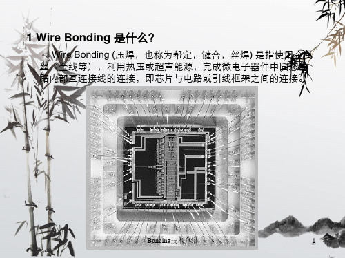
引线键合(WireBonding)

引线键合(WireBonding)引线键合(Wire Bonding)——将芯片装配到PCB上的方法 | SK hynix Newsroom结束前工序的每一个晶圆上,都连接着500~1200个芯片(也可称作Die)。
为了将这些芯片用于所需之处,需要将晶圆切割(Dicing)成单独的芯片后,再与外部进行连接、通电。
此时,连接电线(电信号的传输路径)的方法被称为引线键合(Wire Bonding)。
其实,使用金属引线连接电路的方法已是非常传统的方法了,现在已经越来越少用了。
近来,加装芯片键合(Flip Chip Bonding)和硅穿孔(Through Silicon Via,简称TSV)正在成为新的主流。
加装芯片键合也被称作凸点键合(Bump Bonding),是利用锡球(Solder Ball)小凸点进行键合的方法。
硅穿孔则是一种更先进的方法。
为了了解键合的最基本概念,在本文中,我们将着重探讨引线键合,这一传统的方法。
一、键合法的发展历程图1. 键合法的发展史:引线键合(Wire Bonding)→加装芯片键合(Flip Chip Bonding)→硅穿孔(TSV)下载图片为使半导体芯片在各个领域正常运作,必须从外部提供偏压(Bias voltage)和输入。
因此,需要将金属引线和芯片焊盘连接起来。
早期,人们通过焊接的方法把金属引线连接到芯片焊盘上。
从1965年至今,这种连接方法从引线键合(Wire Bonding),到加装芯片键合(Flip Chip Bonding),再到TSV,经历了多种不同的发展方式。
引线键合顾名思义,是利用金属引线进行连接的方法;加装芯片键合则是利用凸点(bump)代替了金属引线,从而增加了引线连接的柔韧性;TSV作为一种全新的方法,通过数百个孔使上下芯片与印刷电路板(Printed Circuit Board,简称PCB)相连。
二、键合法的比较:引线键合(Wire Bonding)和加装芯片键合(Flip Chip Bonding)图2. 引线键合(Wire Bonding) VS加装芯片键合(Flip Chip Bonding)的工艺下载图片三、引线键合(Wire Bonding)是什么?图3. 引线键合的结构(载体为印刷电路板(PCB)时)下载图片引线键合是把金属引线连接到焊盘上的一种方法,即是把内外部的芯片连接起来的一种技术。
Bonding技术介绍
Ball Bonding(球焊)和 Wedge Bonding (平焊/楔焊)
2.1 Ball Bonding ( 球焊) 金线通过空心夹具的毛细管穿出,然后经过电弧放电使伸出
部分熔化,并在表面张力作用下成球形,然后通过夹具将球压焊 到芯片的电极上,压下后作为第一个焊点,为球焊点,然后从第 一个焊点抽出弯曲的金线再压焊到相应的位置上,形成第二个焊 点,为平焊(楔形)焊点,然后又形成另一个新球用作于下一个 的第一个球焊点。
26
6 压焊工艺的评估:
通常,对压焊效果的评估有两种方法: 外观检查及机械测试 6.1 外观检查
外观检查主要通过光学显微镜,电子显微扫描(SEM),X 射线探测等 手段来实现。 SEM 探测图(良好的球焊效果及月牙形的尾部)
Bonding技术介绍
27
6.2 机械测试 最常用的机械测试方法有两种: 拉力测试和焊球剪切测试
照明
温湿度
4.3 焊接表面的清洁
金线的储存条件 氩等离子 紫外线
N2 微量的污染都会影响 可靠性和焊接性
溶剂清洁
4.4 压焊金属线的物理性质
金属线的硬度
金属线的拉伸强度
合金成B分onding技术介绍
24
Bonding技术介绍
25
只有充分考虑以上因素,才能有效控制压焊工序,才能获得高精度, 高可靠性,高强度,和有竞争力价格的压焊产品。
要表现在以下几个方面: 8.2.1 全自动设备已应用于压焊工序 8.2.2 压焊的各项参数都可以精确的进行监控 8.2.3 压焊的速度已达到 100—125ms/焊接 8.2.4 压焊的最小间距已达到 50微米 8.2.5 通过改良压焊头的结构及相应工序,大大提高了压焊的可靠性
Wire-Bonding工艺介绍和Gold-Wire特性

金线焊接工具---劈刀
劈刀决定的一些参数: 1、Bond Pad Pitch
金线焊接工具---劈刀
T--Tip Diameter, BTNK—Bottleneck Height&Angle, CA—Cone Angle Will affect bond pad pitch.
2、1st Bond Diameter
Not move
affect Not affect
Go up with capillary
Form ball when 6000v on it
Not affect Not affect
金线球形焊接工艺介绍
Stage1
Stage2
Stage3
Stage4
Stage5
Stage6
Stage7
Stage8
H—Hole Diameter, ICA—Inner Chamfer Angle CD—Chamfer Diameter Will affect 1st bond diameter
金线焊接工具---劈刀
3、Wire Diameter
H—Hole Diameter
Hole diameter is usually 1.5X wire diameter
wire
Ultrasonic and force
Form ball when 6000v on it
Not affect
Go up to chamfer, affect touch die surface
Not move
Not affect
Form loop shape Not affect
Squashed and form 2nd bond
引线键合
热压焊:金属线过预热至约300至400℃的氧化铝(Al2O3)或 碳 化 钨 ( WC) 等 耐 火 材 料 所 制 成 的 毛 细 管 状 键 合 头 (Bonding Tool/Capillary,也称为瓷嘴或焊针),再以电火 花或氢焰将金属线烧断并利用熔融金属的表面张力效应使 线之末端成球状(其直径约金属线直径之2倍),键合头 再将金属球下压至已预热至约150至250℃的第一金属焊盘 上进行球形结合(Ball Bond)。在结合时,球点将因受压 力而略为变形,此一压力变形之目的在于增加结合面积、 减低结合面粗糙度对结合的影响、穿破表面氧化层及其他 可能阻碍结合之因素,以形成紧密之结合。
29
底面角
4 degree 专门设计用于解决8度或者0度的问题, 建议使用小的键合头
8 degree 一般用途,很好的第二键合点丝线截断能力 15 degree 仅仅用于热压焊,使用较少
30
5
键合头直径 (T)
主要影响第二键合点的强度, 在允许的范围内应该尽可能大, 小键合头适合于较密(细间距) 键合, 小键合头适合于手工操作。
35
36
6
2013/1/14
铝丝
• 纯铝太软而难拉成丝,一般加入 1% Si 或者1% Mg以提 高强度。 • 室温下1% 的Si 超过了在铝中的溶解度,导致Si的偏析, 偏析的尺寸和数量取决于冷却数度,冷却太慢导致更多 的Si颗粒结集。Si颗粒尺寸影响丝线的塑性,第二相是疲 劳开裂的萌生潜在位置。 • 掺1%镁的铝丝强度和掺1% 硅的强度相当。 • 抗疲劳强度更好,因为镁在铝中的均衡溶解度为2%,于 是没有第二相析出。
31
2013/1/14
键合头镀层
光滑涂层 • 较长的使用寿命 , • 要进行抛光 , • 使得第二键合点光亮, • 减少金属的残留和聚集
WireBonding工艺以和基本知识PPT培训课件
Ball Offset
Capillary Center line
Ball Center line
die 的方 向
lead 的方向
Capillary center -60
Capillary center 60
计算线长 Calculate d Wire Length
DI E
线夹关上 - WIRE CLAMP CLOSE
焊头向上运动 BOND HEAD MOVE UP
CONFIDENTIAL
8. 搜索延遲
搜索延迟 - XY 工作台向第二压点移动 - 焊头不动 SEARCH DELAY - XY TABLE MOVE TOWARDS 2ND BOND - BH MOTIONLESS
动作 焊头下降至第一焊点 之搜索高度 第一焊点之搜索 第一焊点的接触阶段 第一焊点的焊接阶段 返回高度 返回距离 估计线长高度 搜索延迟 焊头下降至第二焊点 之搜索高度 第二焊点之搜索 第二焊点的接触阶段 第二焊点的焊接阶段 线尾长度 焊头回到原始位置
CONFIDENTIAL
焊头動作步驟 1. 焊头在打火高度( 复位位置 )
焊头向上运动 BOND HEAD MOVE UP
反向高度 - RH DIE
CONFIDENTIAL
6. 反向距离
线夹打开 WIRE CLAMP“Open”
反向距离-RD
DIEIE
XY 工作台运动 X-Y TABLE MOVEMENT
CONFIDENTIAL
7. 焊头上升到线弧高度位置
线夹关上后, 开始第一点压 焊检测 M/C START TO DO THE 1ST BOND NON STICK DETECTION AT LOOP TOP POSITION AFTER W/C CLOSE
Wire Bonding Summary
The Nordic Electronics Packaging Guideline Chapter A: Wire BondingLIST OF CONTENTS1. LEVEL 1. INTRODUCTION OF WIREBONDING TECHNOLOGY (2)1.1 W HAT IS WIREBONDING (2)1.1.1 Wirebonding processes (2)1.1.2 Wirebond forms (2)1.3 H ISTORY AND APPLICATIONS (3)1.4 C OST (3)1.5 L IMITATION OF WIREBONDING (4)2 LEVEL 2. CONCLUSIONS AND GUIDELINE (4)2.1 W IREBONDING TECHNIQUES (4)2.1.1 Ball bonding (4)2.1.2 Wedge bonding (5)2.2 W IRES AND TYPICAL METALLURGICAL SYSTEMS (5)2.2.1 Wires usually used in wirebonding (5)2.2.2 Metallurgical systems (6)2.3 B ODING EQUIPMENT (8)2.3.1 Wirebonder (8)2.3.2 Bonding tools (8)2.4 W IREBONDING GUIDELINE (9)2.4.1 Process optimization (9)2.4.2 Wirebonding design (10)2.4.3 Bond evaluation (12)2.5 F AILURE MECHANISMS OF WIREBONDS (16)2.5.1 Failure shooting (16)2.5.2 Pad cleanliness (16)2.5.3 Bonding failures (17)2.5.4 Reliability failures (18)3 LEVEL 3. BACKGROUND INFORMATION (LINKS) (20)3.1 R EPORT (20)3.2 P UBLICATION.........................................................................................F EL! B OKMÄRKET ÄR INTE DEFINIERAT.4 REFERENCES (20)Wirebonding1.Level 1. Introduction of wirebonding technologyThis guideline is concerned with wirebonding technology, which affords the fundamental knowledge and the practical applications to those who are using this technique as well as those who are interested in this technique. This guideline is divided into different levels according to reader’s requirements.1.1What is wirebondingWirebonding is an electrical interconnection technique using thin wire and a combination of heat, pressure and/or ultrasonic energy. Wirebonding is a solid phase welding process, where the two metallic materials (wire and pad surface) are brought into intimate contact. Once the surfaces are in intimate contact, electron sharing or interdiffusion of atoms takes place, resulting in the formation of wirebond. In wirebonding process, bonding force can lead to material deformation, breaking up contamination layer and smoothing out surface asperity, which can be enhanced by the application of ultrasonic energy. Heat can accelerate Interatomic diffusion, thus the bond formation.1.1.1Wirebonding processesWirebonding process begins by firmly attaching the backside of a chip to a chip carrier using either an organic conductive adhesive or a solder (Die Attach). The wires then are welded using a special bonding tool (capillary or wedge). Depending on bonding agent (heat and ultrasonic energy), the bonding process can be defined to three major processes: thermocompression bonding (T/C), ultrasonic bonding (U/S), and thermosonic bonding (T/S), as shown in Table 1-1.Table 1-1. Three wirebonding processes.Wirebonding Pressure Temperature Ultrasonic energy Wire Pad Thermocompression High300-500 o C No Au,Al, Au Ultrasonic Low25 o C Yes Au, Al Al, Au Thermosonic Low100-150 o C Yes Au Al, Au1.1.2Wirebond formsThere are two basic forms of wirebond: ball bond and wedge bond, the corresponding bonding technique, bonding tool and materials are listed in Table 1-2. Currently, thermosonic gold ball bonding is the most widely used bonding technique, primarily because it is faster than ultrasonic aluminum bonding. Once the ball bond is made on the device, the wire may be moved in any direction without stress on the wire, which greatly facilitates automatic wire bonding, as the movement need only be in the x and y directions.Ball bondWedge bondTable 1-2. Wirebond formation.Wirebond Bonding technique Bonding tool Wire Pad Speed Ball bond T/C, T/S Capillary Au Al, Au10 wires/sec (T/S) Wedge bond T/S, U/S Wedge Au, Al Al, Au 4 wires/sec1.3History and applicationsWirebonding is the earliest technique of device assembly, whose first result was published by Bell Laboratories in 1957. Sine then, the technique has been extremely developed:•Fully automatic machines have been developed for volume production.•Bonding parameters can be precisely controlled; mechanical properties of wires can be highly reproduced.•Bonding speed can reach 100-125 ms per each wire interconnection (two welds and a wire loop).•Bond pitch of 50 µm and the consistent loop with less than 40 µm have been achieved.•Most reliability problems can be eliminated with properly controlled and much improved tools (capillaries and wedges) and processes.•Specific bonding tools and wires can be selected by packaging engineers to meet the requirements.•Infrastructure of the technique has been comprised by large wirebonding knowledge, manufacturing people, equipment venders and materials.As a result, a reliable and completely repeatable bond formation process can be produced.Owing to its potentially low cost, its much improved yields and reliability, wirebonding, as the dominant chip-connection technology, has been used with all styles of microelectronic packages, from small individual chip packages to large, high-density multichip modules. The most popular applications that use wirebonding are:•Single and multitiered cofired ceramic and plastic ball grid arrays (BGAs), single chip and multichip •Ceramic and plastic quad flat packages (CerQuads and PQFPs)•Chip scale packages (CSPs)•Chip on board (COB)V irtually all dynamic random access memory (DRAM) chips andmost commodity chips in plastic packages are assembled bywirebonding. About 1.2-1.4 trillion wire interconnections areproduced annually. Manufacturing losses and test failures areabout 40-1000 ppm and trending downward each year. It isbelieved that wirebonding will continue to dominate memory andcommodity packaging requiring relatively small I/O counts (< 500I/O) in the future. In addition, wirebonding method is used toconnect other components, such as resistors or capacitors, tosubstrate, package terminals to substrate, or one substrate toanother.1.4CostThe main cost of wirebonding method includes:•Wirebonder.•Die attach equipment.•Support equipment, such as wire pull and shear stations, plasma etchers, as well as storage facilities.•Materials including tool, wire, die attach materials.•Engineering.Wirebonding is a low cost process since:•No chip modification is needed.•Equipment has an established base of competitive development.•Substantial non-recurring engineering (NRE) charge and tooling charge are minimized.Cost analysis should include volume and individual process cycle time predictions. In some cases, the cost associated with the flexibility required for engineering and product design charges, which occur and should be anticipated as a part of the planing cycle, also should be evaluated.1.5Limitation of wirebondingFor the application of wirebonding method, terminals of chips have to be arranged at the periphery of the chips, otherwise short circuit is easily caused. Therefore, wirebonding technique is difficult for high I/O(>500) interconnections.2Level 2. Conclusions and guideline2.1 Wirebonding techniquesT here are two basic wirebonding techniques that are used in thermocompression (T/C), thermosonic (T/S) or ultrasonic (U/S) bonding process: ball bonding and wedge bonding. Approximately 93% of all semiconductor packages are manufactured using ball bonding method, while wedge bonding is used to produce about 5% of all assembled packages.2.1.1Ball bondingI n this technique, wire is passed through a hollow capillary, and anelectronic-flame-off system (EFO) is used to melt a small portionof the wire extending beneath the capillary. The surface tension ofthe molten metal from a spherical shape, or ball, as the wirematerial solidifies. The ball is pressed to the bonding pad on thedie with sufficient force to cause plastic deformation and atomicinterdiffusion of the wire and the underlying metallization, whichensure the intimate contact between the two metal surfaces andform the first bond (ball bond). The capillary is then raised andrepositioned over the second bond site on the substrate, aprecisely shaped wire connection called a wire loop is thus createdas the wire goes. Deforming the wire against the bonding padmakes the second bond (wedge bond or stitch bond), having acrescent or fishtail shape made by the imprint of the capillary’souter geometry. Then the wire clamp is closed, and the capillaryascends once again, breaking the wire just above the wedge, an exact wire length is left for EFO to form a new ball to begin bonding the next wire. Ball bonding is generally used in thermocompression (T/C) or thermosonic bonding (T/S) process. This technique requires a high temperature raging from 100o C to 500o Cdepending on bonding process. Heat is generated during themanufacturing process either by a heated capillary feeding the wireor by a heated pedestal on which the assembly is placed or by bothdepending on the bonding purpose and materials. Relatively smallgold wire (< 75 µm) is mostly used in this technique because of itseasy deformation under pressure at elevated temperature, itsresistance to oxide formation, and its ball formability during aflame-off or electronic discharge cutting process. Ball bonding isgenerally used in application where the pad pitch is greater than100 µm. However, the application of the pitches with 50 µm hasbeen reported.2.1.2Wedge bondingW edge bonding is named based on the shape of its bonding tool. In this technique, the wire is fed at an angle usually 30-60o from the horizontal bonding surface through a hole in the back of a bonding wedge. Normally, forward bonding is preferred, i.e. the first bond is made to the die and the second is made to the substrate. The reason is that it can be far less susceptible to edge shorts between the wire and die. By descending the wedge onto the IC bond pad, the wire is pinned against the pad surface and an U/S or T/S bond is performed. Next, the wedge rises and executes a motion to create a desired loop shape. At the second bond location, the wedge descends, making asecond bond. During the loop formation, the movementof the axis of the bonding wedge feed hole must bealigned with the center line of the first bond, so that thewire can be fed freely through the hole in the wedge.Several methods can be used to end the wire after thesecond bond. For small wires (<75 µm), clamps can beused to break the wire while machine bonding force ismaintained on the second bond (clamp tear), or theclamps remains stationary and the bonding tool raisesoff the second bond to tear the wire (table tear). Theclamp tear process offers a slightly higher yield andreliability than the table tear process due to the forcemaintained on the second bond during the clamp tearmotion. The clamp tear process also offers a light speed advantage over the table tear process due to fewer required table motions. However, the table tear process,with a higher wire feed angle capability and stationaryclamp, has the potential to provide slightly moreclearance from package obstructions such as a bondshelf or pin grid. For large bonding wires (>75 µm), othermethods can be used such as a cutting blade or theplacement of the wire into a channel in the wedge forwire termination. As the wedge ascends, the clampedwire is fed under it to begin bonding the next wire.W edge bonding technique can be used for bothaluminum wire and gold wire bonding applications. Theprinciple difference between the two processes is that the aluminum wire is bonded in an ultrasonic bonding process at room temperature, whereas gold wire wedge bonding is performed through a thermosonic bonding process with heating up to 150o C. A considerable advantage of the wedge bonding is that it can be designed and manufactured to very small dimensions, down to 50 µm pitch. However, factors based on machine rotational movements make the overall speed of the process less than thermosonic ball bonding. Aluminum ultrasonic bonding is the most common wedge bonding process because of the low cost and the low working temperature. The main advantage for gold wire wedge bonding is the possibility to avoid the need of hermetic packaging after bonding due to the inert properties of the gold. In addition, a wedge bond will give a smaller footprint than a ball bond, which specially benefits the microwave devices with small pads that require a gold wire junction.2.2Wires and typical metallurgical systemsG old and aluminum are the commonly used wire materials, in addition, copper and silver have also been used. Bonding these wires to different pad materials produces different metallurgical systems.2.2.1Wires usually used in wirebondingGold wireG old wire is used extensively for thermocompression bonding and thermosonic bonding. In producing the gold bonding wires, surface finish and surface cleanliness are the critical issues to ensure the formation of a strong bond and to prevent clogging of bonding capillaries. Pure gold can usually be drawn to produce an adequate breaking strength (ultimate tensile strength of the wire) and proper elongation (ratio of the increase in wire length at rupture to the initial wire length given as a percentage) for use as bond wire. Ultrapure gold is very soft, therefore small amounts of impurities such as 5-10 ppm by weight of Be or 30-100 ppm by weight of Cu are added to make the gold wire workable. Be-doped wire is stronger than Cu-doped wire by about 10-20% under most conditions, thus advantageous for automated thermosonic bonding where high-speed capillary movements generate higher stresses than in slow or manual bonders.Aluminum wireP ure aluminum is typically too soft to be drawn into a fine wire. Therefore, aluminum is often alloyed with 1% Si or 1% Mg to provide a strengthening mechanism. At room temperature, 1% silicon exceeds the solubility of silicon in aluminum by a factor of 50, which leads to silicon precipitation. The number and the size of the silicon precipitates are dependent on the cooling rate from higher temperatures. Slower cooling rates result in more precipitation and large nonuniform silicon nodules, while faster cooling rates do not allow sufficient time for silicon precipitation resulting is uniformly dispersed nodules. Silicon grain size can affect wire ductility, the second phase can become a potential nucleation site for fatigue cracks.A luminum alloyed with 1% magnesium can be drawn into a fine wire that exhibits a breaking strength similar to that of Al-1% Si. The Al-1% Mg alloy wire bonds satisfactorily and is superior to Al-1% Si in resistance to fatigue failure and to degradation of ultimate strength after exposure to elevated temperatures. These advantages of Al-1% Mg wire occur because the equilibrium solid solubility of Mg in Al is about 2% by weight, and thus at 0.5-1% Mg concentration there is no tendency towards second-phase segregation as is the case with Al-1% Si.Copper wireR ecently, copper-ball bonding to IC metallization has received considerable attention primarily because of their economy and their resistance to sweep (tendency of the wire to move in the plane perpendicular to its length) during plastic encapsulation. The major problem for this system is the bondability. Copper is harder than gold and aluminum, which can lead to cratering or pushing the metallization aside. Therefore a harder metallization is required. In addition, the ball bonding must be performed in an inert atmosphere as copper oxidizes readily.2.2.2Metallurgical systemsIn wirebonding process, different pad metallizations are used, depending to the production requirements. Therefore, different metallurgical systems can be formed with different reliability behaviours. The typical metallurgical systems are:A u-Au systemG old wire bonded to a gold bond pad is extremely reliable because the bond is not subject to interface corrosion, intermetallic formation, or other bond-degrading conditions. Even a poorly welded gold-gold bond will increase in strength with time and temperature. Gold wire welds best with heat although cold ultrasonic Au-Au wire bonds can be made. Either thermocompression or thermosonic bonds are easily and reliably made. Thermocompression bondability, however, is strongly affected by surface contamination.A u-Al systemA u-Al welding system is the most commonly used in wirebonding process. However, this bonding system can easily lead to formation of Au-Al intermetallic compounds and associated Kirkendall voids. The formation can be accelerated with the temperature and time of the operational life. There are five intermetallic compounds that are all colored: Au5Al2 (tan), Au4Al (tan), Au2Al (metallic gray), AuAl (white), and AuAl2 (deep purple). AuAl2 can initially form in the interface between gold and aluminum during bonding process even at room temperature and could transform to other Au-Al compounds depending on the temperature, time and bonding configurations. Therefore, this system often presents a problem in reliability of the bonds.A u-Cu systemB onding gold wires to bare copper lead frames can cause the formation of three ductile intermetallic phases (Cu3Au, AuCu, and Au3Cu) with overall activation energies of 0.8 to 1 eV. The formation of these intermetallic compounds can decrease the bond strength at higher temperatures (200-325o C) as a result of Kirkendall voiding. The degradation is apparently dependent on the microstructure, weld quality, and impurity content of the copper. Cleanliness of the bonding surface is extremely important to ensure goodbondability and reliability in Cu-Au systems. In addition, if polymer material is used for die attach, the polymer must be cured in an inert atmosphere to prevent oxidation.A u-Ag systemT he Au-Ag wire bond-system is very reliable for very long times at high temperatures. This bond system does not form intermetallic compounds and does not exhibit interface corrosion. Gold-wire bonds to silver-plated lead frames have been successfully used in high production for many years. Bondability problems can be caused by contaminants like sulfur. Thermosonic Au-Ag bonding is usually performed at high temperature (approximately 250o C) which dissociates thin silver-sulfide films thus increases bondability of silver.A l-Al systemT he aluminum- aluminum wire bond system is extremely reliable because it is not prone to intermetallic formation and corrosion. Aluminum wire on aluminum metallization weds best ultrasonically, although a thermocompression bond can be produced by high deformation.A l-Ag systemA luminum wire bonded to a silver-plated lead frame is often used in thick-film hybrids (usually in alloy form with Pt or Pd). The Ag-Al phase diagram is very complex, with many intermetallic phases. Kirkendall voids can occur in this metal system, but typically at temperatures higher than the operating range of the microcircuits. In practice, Ag-Al bonds are seldom used because of their tendency to degrade due to interdiffusion and to oxidize in the presence of humidity. Chlorine is the main driving element of the corrosion process. Aluminum wires with large diameters are routinely bonded to Pd-Ag thick-film metallization in automotive hybrids. However, the bonding surface must be prepared by washing with solvents, followed by careful resistivity-monitored cleaning in deionized water. Then the hybrids are covered with a silicone gel for further protection.A l-Ni systemA l-Ni bonds using large diameter, >75 µm, aluminum wires are less prone to Kirkendall voiding and galvanic corrosion, thus more reliable than Al-Ag or Al-Au bonds under various environments. This system has been used in high production on power devices and high-temperature applications such as aircraft turbine blades for over fifteen years. In most cases, the nickel is deposited from electroless boride or sulfamate solutions, which results in reliable bonds. However, phosphide electroless nickel solutions that co-deposit more than 6 or 8% of phosphorous can result in both reliability and bondability problems. The main difficulty encountered when bonding to nickel plating is bondability rather than reliability due to nickel surface oxidation. Thus, packages should be bonded soon after they are Ni-plated, protected in an inert atmosphere, or chemically cleaned before bonding. Changing bonding machine schedules, such as impacting the tool-wire-plating with the ultrasonic energy applied, can improve bondability to slightly oxidized nickel surfaces. Various surface preparation techniques (such as sandblasting) are sometimes applied before or after Ni plating to increase bondability.C u-Al systemC opper wire can be bonded to both gold and aluminum substrate. Au-Cu system has been discussed before. For Cu-Al system, there exist five intermetallic compounds favoring the copper-rich side. Thus, there is the possibility of various intermetallic failures similar to those of Au-Al system. However, intermetallic growth in Cu-Al bonds is slower than in Au-Al bonds. The intermetallic growth in Cu-Al bonds does not result in Kirkendall voiding bur lowers the shear strength at 150-200o C due to the growth of a brittle CuAl2 phase. In the temperature range 300-500o C, bond strength significantly decreases with the increase of the total intermetallic thickness. The rate of Cu-Al intermetallic formation relies on the ambient atmosphere composition. For example, the copper-aluminum bond system is adequately reliable as long as some oxygen is present in the package because Cu oxide prevents or inhibits the growth of void-like grooves under the bond. However, the presence of Cl contamination and water can cause corrosion of the aluminum metallization containing copper-aluminum intermetallics.2.3Boding equipment2.3.1WirebonderA lthough other connection technologies have gained popularity, wirebonding technique can still maintain its competitive position owing to the massive equipment infrastructure of wirebonding. The bonding equipment is continuously improved by increasing bonding rates, decreasing bond pad pitch, and increasing operation stability. Now, speeds of 4 wires/sec for wedge bonding and 10 wires/second for ball bonding are common, high strength and low variability are achieved and maintained. Many types of analytical equipment are used to monitor wirebonder performance. The bonding location can be accurately determined by vision and positioning systems of the equipment. Fully automated equipment has been manufactured, which is available to measure the impedance of the bonding tool in free air and as the bond is formed. These impedance measurements can be used to maximize the performance of the ultrasonic system and to troubleshoot the system. Another wirebonding equipment feature beneficial to manufacturing is the capability to change quickly from one product to another with minimal tooling and software changes. Software programs for a wide variety of products can be written by the user and stored on disk. A product change can be made in as little as 20 minutes.2.3.2Bonding toolsW edgeW edge bonding is performed using a wedge-shaped bonding tool. The wire in wedge bonding is addressed at an angle (30o to 60o) through the rear of the wedge. Low angle wire feed style gives best placement control and tail consistency under the bond foot. High angle is only used when absolutely necessary due to high package walls or other tall devices in the bonding vicinity. In the case of high angle wire feed, tail control is less consistent due to the steep feed angle and the action of the clamps. This gives the system a limitation on its access for pads close to deep walled packages. Foot profile of the wedge can be either flat or concave. Most of the automatic aluminum wire applications use concave foot to reduce wire positioning errors. The flat foot is used mainly with gold wire, or with aluminum wire, to obtain extremely short bonds. Recently, a groove foot has been designed for gold wire wedge bonding to improve the wedge-to-wire gripping. The material used for the wedge is dependent on the bonding wire material. For aluminum wire, the wedge is usually made of tungsten carbide or ceramic. The ceramic wedges are relatively new and give improved quality and tool life, however the price is high. For gold wire, the material used is titanium carbide as the gold leaches out the cobalt binder in the tungsten carbide wedge. Tungsten may be used but its life will be greatly reduced. The parameters of the wedge can greatly affect the wirebond characteristics. For the first bond, pull strength is affected by back radius (BR), bond location is influenced by hole size (H), tail length is controlled by feed angle, hole shape and surface quality. The main wedge parameters that affect looping are hole size and shape, as well as feed angle. For the second bond, pull strength is defined mainly by front radius (FR) and bond length, and tail consistency is affected by back radius (BR).CapillaryWedge for Al wire wedge bondingWedge for Au wire sedge bondingtungsten or ruby materials. The most common material forcapillaries is high density fine grain alumina ceramic because of itshigh wear resistance, high oxidation resistance and easy cleaning.A polish finish produces a shiny bond, used when there is goodbondability, whereas a matte finish produces a textured stitch bond,which is used when there is less than good bondability. Thecapillaries are typically 1.585 mm in diameter and 11.1 mm long.They have a large entry hole at the top and then the hole tapersdown to a small hole diameter typically between 38-50 µm,depending upon the wire diameter used and the application. At theexit of the small hole, there is normally an inside chamfer (IC) orinside radius (IR). The inside chamfer is designed to seat the ball inthe tool and to provide good downward force. A 120o chamfer isdesigned for poor bondable surfaces by providing more downwardCapillary for ball bondingforce. The disadvantage is that it puts more drag on the wire. A 90ochamfer is designed for easily bondable surfaces giving equaldownward and holding forces. There is relatively little drag. The double inside chamfer capillary was introduced to combine the qualities of the 90o and 120o tools. Recently, 70o chamfer is also used for special small ball, fine pitch applications.2.4 Wirebonding guideline2.4.1Process optimizationT o develop and improve a production, the key stages generally include initial process design and development, process characterization, process control, as well as process optimization. These stages forma continuous loop between characterization and control, with periodic optimization and development, asshown in the following procedure diagram.T ypical wire bond process development flowchartI n the initial stages of the process, process capabilities should be known to set achievable goals. The related information can be obtained from laboratory studies, published literature, as well as from industry and equipment vendor experiences. The second stage (process characterization) is to collect and categorize the data on wirebonding failures such as bond off center, bond not sticking on die, wire breaking and so on. Process control (the third stage) is important for a successful process. To achieve a stable performance, the operating variables such as bond program parameters, machine setup and operation procedures, bonding tool installation, wire pull procedures and product change must be minimized and strict regulation of the existing variables must be established. Consistency across the process, such as in the training of operators also must be established. If the previous stages of process development are in place, process optimization。
wire-bonding--介绍

Welding Time (Bond Time)
Welding Tempature (Heater)
THERMAL BONING
Thermal Compressure
2021/6/7 Ultrasonic Energy (Power)
7
Bond Head ASSY
• Low impact force •Real time Bonding Force monitoring • High resolution z-axis position with 2.5 micron per step resolution • Fast contact detection • Suppressed Force vibration • Fast Force response • Fast response voice coil wire clamp
Solder Ball Placement
Dejunk TRIM Solder Plating
Singulation
Solder Plating TRIM/ FORMING
Dejunk TRIM
Packing 4
Wire Bond 原理
Ball Bond ( 1st Bond )
Wedge Bond ( 2nd Bond )
2021/6/7
12
Eagle
MACHINE SPECIFICATIONS (III)
•Material Handling System •Indexing Speed 200 – 250 ms @ 0.5 “ pitch •Indexer Resolution 1um •Leadframe Position Accuracy + 2 mil •Applicable Leadframe W = 17 – 75 mm @ bonding area in Y = 65mm
qfn封装wire bongding设计规则-概述说明以及解释

qfn封装wire bongding设计规则-概述说明以及解释1.引言1.1 概述概述部分的内容将简要介绍本文所涉及的主题——qfn封装wire bongding设计规则,并对文章结构和目的进行概括说明。
概述:QFN封装是一种广泛应用于电子元件的封装形式,它具有小尺寸、低成本、良好的热传导性能等特点,已经成为现代电子设备中常见的封装选择之一。
在QFN封装中,wire bonding是一项非常关键的步骤,它涉及到在芯片和封装基座之间通过金属线进行连接。
而qfn封装wire bonding 设计规则则是指在进行wire bonding过程中,需要遵循的一系列设计准则和原则,以确保连接的可靠性和稳定性。
文章结构:本文将围绕qfn封装wire bongding设计规则展开讨论,分为三个主要部分:引言、正文和结论。
引言部分将对文章的背景和目的进行介绍,正文部分将详细阐述qfn封装wire bongding设计规则的重要性、基本原则和具体要点,结论部分将对文章进行总结,并展望未来qfn封装wire bongding设计规则的发展。
目的:本文的目的是探讨qfn封装wire bongding设计规则在电子封装领域的重要性,为相关领域的从业者和研究人员提供有关于qfn封装wire bongding设计规则的基本知识和具体要点。
通过对qfn封装wire bongding设计规则的讨论和总结,本文旨在提高电子封装领域从业者对该规则的认识和理解,以减少因设计不当而导致的不良连接和可靠性问题。
同时,本文也将展望未来qfn封装wire bongding设计规则的发展趋势,为该领域的进一步研究和应用提供参考和启示。
1.2 文章结构文章结构部分的内容可以包括以下信息:文章结构部分旨在为读者介绍本文的整体结构,使读者对文章的内容有一个清晰的了解。
本文分为引言、正文和结论三个部分。
引言部分首先概述了文章的主题和重要性,然后介绍了文章的结构和目的。
Wire-Bonding工艺以及基本知识参考幻灯片
Smaller CD – Smaller
MBD
Bigger CD – Bigger
MBD
CD MBD
CA:70(Degree
)
CD MBD
CA:120(Degre
e)
将Chamfer角由90°变更為120°可使Ball形状变大,随之 Ball的宽度变宽、与Pad接合面積也能变宽。
Chamfer Angle:90°
Chamfer Angle:120°
CONFIDENTIAL
3. OR(Outer Radius)及FA(Face Angle): 对Hill Crack、Capillary的OR(Outer Radius)及FA(Face Angle)的數值是重要影響因素
2nd Neck部 Crack発生ห้องสมุดไป่ตู้
荷重过度附加接触面导致破损 Crack発生
1/16 inch 總長L
CONFIDENTIAL
Capillary尺寸對焊線品質的影響:
1. Chamfer径(CD) Chamfer径过于大的话、Bonding強度越弱,易造成虛焊.
CD
CD
CONFIDENTIAL
2. Chamfer角(ICA ) Chamfer角:小→Ball Size:小 Chamfer角:大→Ball Size:大
CONFIDENTIAL
3.Bonding用 Capillary
Capillary的選用:
Hole径(H)
Hole径是由规定的Wire径WD(Wire Diameter)
来決定
H
H=1.2~1.5WD
WD
Capillary主要的尺寸:
H:Hole Diameter (Hole径) T:Tip Diameter B:Chamfer Diameter(orCD) IC:Inside Chamfer IC ANGLE:Inside Chamfer Angle FA:Face Angle (Face角) OR:Outside Radius
Wire-Bonding工艺以及基本知识

A. 15(15XX):直徑1/16 inch (約1.6mm),標準氧化鋁陶瓷 B. XX51:capillary產品系列號 C. 18: Hole Size 直徑為0.0018 in.(約46μm ) D. 437:capillary 總長0.437 in.(約11.1mm) E. GM: capillary tip無拋光; (P: capillary tip有拋光) F. 50: capillary tip 直徑T值為0.0050 in. (約127μm) G. 4: IC為0.0004 in. (約10μm) H. 8D:端面角度face angle為 8° I. 10:外端半徑OR為0.0010 in.(約25μm) J. 20D:錐度角為20° K. CZ1:材質分類,分CZ1,CZ3,CZ8三種系列
1.Wire Bonding原理
IC封裝中電路連接的三種方式: a. 倒裝焊(Flip chip bonding) b. 載帶自動焊(TAB---tape automated bonding) c. 引線鍵合(wire bonding)
Wire Bonding------引線鍵合技術
Wire Bonding的作用
线夹 打开– Wire Clamp Open
在第一焊点搜索高度开始, 焊头使用固定的 速度搜索接触高度 At Search Height Position Bond Head Switch to Constant Speed(Search Speed) to Search For Contact
第一焊点搜索高度1st Search Height
Smaller CD – Smaller
MBD
Bigger CD – Bigger
MBD
Wire_Bonding_的基础

Ball Bonder Ball Bonder (装置技術) (装置技術)
Ball Bonding Ball Bonding
Capillary Capillary Bonding技術 Bonding技術 (Process技術) (Process技術)
3
3.Bonding用 Wire
3-1 Au Wireの主要特征
14
FA(Face Angle)変更0°→8°変更来抑制与接触面過度强加荷重。 OR(Outer Radius):0.0035inch 同一 用FA変更的Wire Pull強度面确认不到有意差,但如下記图片,2nd Neck部的状態比较稳定。
FA=0°、MIN条件
FA=0°、MAX条件
FA=0°、TYP条件
Wire Bonding 的基礎
目录 1.Wire Bonding種類 2.Ball Bonding実現手段 3.Bonding用 Wire 4.Bonding用 Capillary 5.Ball Bonding Process的概要 6.超声波 7.FAB(Free Air Ball)形成 8.Wire Pull Test 9.Wire Bonding稳定化
高温破断強度(cN)
線径:25μm Bonder:CUB-10 (Reverse無し) ●:高Loop □:中Loop △:低Loop
◇:超低Loop 高温条件: 250℃X20sec 根据Mitsubishi Materials的資料転載
熱影響領域(再結晶領域)
5
3-3 对Au Wire的要求
对Au Wire的要求、除純度以外 寸法的精度要高(用0.1um制御可能) 寸法的精度要高(用0.1um制御可能) 表面要圆滑、金属要有光泽 表面要圆滑、金属要有光泽 表面不能有灰尘、污染 表面不能有灰尘、污染 具有拉伸强度、要有一定的弹性 具有拉伸强度、要有一定的弹性 Curl(卷曲性)要小 Curl(卷曲性)要小 Au Wire前端形成的 Ball的形状要有一定的真圆性 Au Wire前端形成的 Ball的形状要有一定的真圆性 等機能的要求
WireBonding
Wire
Ball Bonder (装置技術)
Ball Bonding
Capillary Bonding技術 (Process技術)
3
3.Bonding用 Wire
3-1 Au Wireの主要特征
主要特征有 在大気中或在水中化学性稳定及非氧化的性質 。 金属中、展延性较好、可加工Bonding用 Wire使用的直径为10 ~38μm程度的極細線。 吸収Gas极其尐 具有对熱压缩 Bonding最适合的硬度 具有耐樹脂 Mold的Stress的機械性強度 具有銀、銅其次的高電気传导性 电阻率(μΩ・cm)的比較 Ag(1.6)<Cu(1.7)<Au(2.3)<Al(2.7) 等、具有良好的化学性、機械性的性質
超声波・熱圧缩并用方式
这种方式是为降低Bonding温度为目 的所開発的。 为补充因温度降低导致 熱Energy減 尐的部分而附加超声波Energy Wedge Bonding
Al、Au Wire 2
2.影响Ball Bonding的要因
Lead Frame /基板 接着剤 半導体 Chip Die Bonder Die Bonding Cure
FA=0°、MIN条件
FA=0°、MAX条件
FA=0°、TYP条件
FA=8°、MIN条件
FA=8°、MAX条件
FA=8°、TYP条件 15
5.Ball Bonding的Process概要
5-1 超声波熱圧缩的Process概要
①Search動作
①
半導体 Chip
(没有Loop Control的情况)
Bigger CD – Bigger MBD
FAB の Centering
接合時的左右荷重・超 音波振動伝達
wire_bonding__介绍
WIRE BONDWIRE BOND PROCESS INTRODUCTIONCONTENTSÂASSEMBLY FLOW OF PLASTIC IC ÂWire Bond 原理M/C IntroductionÂM/C IntroductionÂWire Bond ProcessWire Bond ProcessÂMaterialÂSPECÂCalculatorÂDEFECTG ld Wi晶片Die金線Gold Wire導線架Lead framWafer Grinding Die Bonding Wafer Saw toaster Wire Bonding Die SurfaceCoating Molding Laser MarkSolder BallPlacement SingulationBGA PackingDejunk TRIM SolderPlatingDejunk TRIM SURFACE MOUNTPKG Solder Plating TRIM/FORMING THROUGH HOLE PKGWire Bond 原理Ball Bond Wedge Bond (2d B d)( 1st Bond )( 2nd Bond )Gold wirepadleadB.PRINCIPLEPRESSUREVIBRATION AL2O3MOISTURECONTAMINATIONGOLD BALLGLASSAlSiO2Si銲接條件ÂHARD WELDINGÂPressure (Force)A lif&FÂAmplify & FrequecyÂWelding Time (Bond Time) Welding Time(Bond Time)e d g e patu e(eate)ÂWelding Tempature (Heater)ÂTHERMAL BONINGÂThermal CompressureÂUltrasonic Energy (Power)Bond Head ASSY•Low impact force•Real time Bonding Force monitoringReal time Bonding Force monitoring•High resolution z-axis position with 2.5 micron per step resolutionstep resolution•Fast contact detection•Suppressed Force vibrationSuppressed Force vibration•Fast Force responseF t i il i l•Fast response voice coil wire clampX Y Table•Linear 3 phase AC Servo motorHigh power AC Current Amplifier•High power AC Current Amplifier•DSP based control platform•High X-Y positioning accuracy of +/-1 mm Hi h X Y iti i f/1•Resolution of 0.2 mmW/H ASSY •changeover•· Fully programmable indexer & tracks·Fully programmable indexer&tracks•· Motorized window clamp with soft close feature•· Output indexer with leadframe jam protection feature•Tool less conversion window clamps and top plate enables fast device•Bonding SystemB di M th d Th i (TS)MACHINE SPECIFICATIONS (I)•Bonding Method ÎThermosonic (TS)•BQM Mode ÎConstant Current, Voltage, Power and Normal(Programmable)•Loop Type ÎNormal, Low, Square & J •XY Resolution Î0.2 um•Z Resolution (capillary travelling motion)Î2.5 um •Fine Pitch Capability Î35 mm pitch @ 0.6 mil wire N f B di Wi t 1000•No. of Bonding Wires Îup to 1000•Program Storage Î1000 programs on Hard Disk •Multimode Transducer System •Multimode Transducer SystemÎProgrammable profile, control and vibration modes•Vision System MACHINE SPECIFICATIONS (II)y•Pattern Recognition Time Î70 ms / point •Pattern Recognition Accuracy Î+ 0.37 um •Lead Locator Detection Î12 ms / lead(3 leads/frame)•Lead Locator Accuracy +24um•Lead Locator Accuracy Î+ 2.4 um •Post Bond Inspection ÎFirst Bond, Second BondWire Tracing g•Max. Die Level Different Î400 –500 um •Facilities•Voltage 110 VAC (optional 100/120/200/210/•220/230/240 VAC•Material Handling System MACHINE SPECIFICATIONS (III)g y•Indexing Speed Î200 –250 ms @ 0.5 “ pitch •Indexer Resolution Î1um•Leadframe Position Accuracy +2milLeadframe Position Accuracy Î 2 mil •Applicable Leadframe ÎW = 17 –75 mm @ bonding area in Y = 65mm= 17 –90 mm @ bonding area in Y = 54mmL =280mm [Maximum]L = 280 mm [Maximum]T = 0.075 –0.8 mmApplicable Magazine W =100mm (Maximum)•Applicable Magazine ÎW = 100 mm (Maximum)L = 140 –300 mmH = 180 mm (Maximum)M i Pi h 2410(009”039“)•Magazine Pitch Î 2.4 –10 mm (0.09” –0.39 “)•Device Changeover Î< 4 minutes•Package Changeover Î< 5 minutes•Number of Buffer Magazine Î3 (max. 435 mm)Bonding ProcessgThe Wire BondTempPREHEAT BONDSITE10 200+/--10 CU L/F200+/--10 200+/CU L/F200+/10 230+/--10 AL L/F210+/--10 230+/AL L/F210+/BGA 150+/--10 160+/10 160+/--10 BGA 150+/10 160+/--10 TFBGA150+/--10 160+/ TFBGA150+/10160+/ LBGA 150+/--10 160+/10 160+/--10 LBGA 150+/150+/10160+/-LBGA150+/-160+/ NOT INCLUDE DEDICATE LINEi th h fin the chamferppadleadin the chamferi th h fSEARCH HEIGHTpadleadi th h f in the chamferpad SEARCH SPEED1 SEARCH TOL1pleadSEARCH TOL 1in the chamfer in the chamferpad SEARCH SPEED1 SEARCH TOL1pleadSEARCH TOL 1in the chamferin the chamferSEARCH SPEED1SEARCH TOL 1SEARCH TOL1pad leadin the chamferin the chamferSEARCH SPEED1SEARCH TOL 1SEARCH TOL1pad leadin the chamferin the chamferSEARCH SPEED1SEARCH TOL 1SEARCH TOL1pad leadSEARCH SPEED1SEARCH TOL 1SEARCH TOL1pad leadIMPACT FORCESEARCH SPEED1SEARCH TOL 1SEARCH TOL1pad leadContactContactPRESSUREUltraSonicVibrationheatpad leadBaseBasePRESSUREUltraSonicVibrationheatpad leadheight positionheight positionpad leadheight positionheight positionpad leadheight positionheight positionpad leadheight positionheight positionpad leadheight positionheight positionpad leadheight positionheight positionRHpad leadRD (Reverse Distance)()pad leadpad leadpad leadWIRE CLAMPCLOSE‘CLOSE’CalculatedWire Lengthpad leadCalculatedWire Lengthpad leadSEARCHDELAYpad leadTRAJECTORY pad leadTRAJECTORY pad leadTRAJECTORY pad leadTRAJECTORY pad leadTRAJECTORY pad leadTRAJECTORY pad leadTRAJECTORY pad leadTRAJECTORY pad leadTRAJECTORY pad leadTRAJECTORY pad lead2nd Search Height 2nd Search Height Search Speed 2pad leadSearch Speed 2Search Tol 2Search Speed 2pad lead Search Speed 2Search Tol 2。
- 1、下载文档前请自行甄别文档内容的完整性,平台不提供额外的编辑、内容补充、找答案等附加服务。
- 2、"仅部分预览"的文档,不可在线预览部分如存在完整性等问题,可反馈申请退款(可完整预览的文档不适用该条件!)。
- 3、如文档侵犯您的权益,请联系客服反馈,我们会尽快为您处理(人工客服工作时间:9:00-18:30)。
Ultra
Sonic
Vibration
pad
heat
lead
Formation of a first bond Base
PRESSURE
Ultra Sonic Vibration
pad
heat
lead
Capillary rises to loop height position
pad
WIRE BOND PROCESS INTRODUCTION
CONTENTS
ASSEMBLY FLOW OF PLASTIC IC Wire Bond 原理 M/C Introduction Wire Bond Process Material SPEC Calculator DEFECT
pad
lead
TRAJECTORY
pad
lead
TRAJECTORY
pad
lead
TRAJECTORY
pad
lead
TRAJECTORY
pad
lead
TRAJECTORY
pad
lead
2nd Search Height
pad
Search Speed 2 Search Tol 2
leadpຫໍສະໝຸດ dleadCapillary rises to loop height position
pad
lead
Capillary rises to loop height position
pad
lead
Capillary rises to loop height position
pad
lead
Capillary rises to loop height position
Formation of a second bond Base
pad
heat
lead
pad
lead
pad
lead
pad
lead
Tail length
pad
lead
pad
lead
pad
lead
Disconnection of the tail
pad
lead
Disconnection of the tail
(SPT, GAISER, PECO, TOTO…)
Capillary Data
( Tip , Hole , CD , FA&OR , IC )
CAPILLARY (II)
Calculated
Wire Length
pad
lead
Calculated
Wire Length
pad
lead
SEARCH DELAY
pad
lead
TRAJECTORY
pad
lead
TRAJECTORY
pad
lead
TRAJECTORY
pad
lead
TRAJECTORY
pad
lead
TRAJECTORY
X Y Table
•Linear 3 phase AC Servo motor •High power AC Current Amplifier •DSP based control platform •High X-Y positioning accuracy of +/- 1 mm •Resolution of 0.2 mm
Bonding Process
PREHEAT
The Wire Bond Temp
BONDSITE
CU L/F200+/-10
AL L/F210+/-10
200+/-10
230+/-10
BGA
150+/-10
160+/-10
160+/-10 160+/-10
TFBGA150+/-10 LBGA 150+/-10
Thermal Compressure
Ultrasonic Energy (Power)
Bond Head ASSY
• Low impact force •Real time Bonding Force monitoring • High resolution z-axis position with 2.5 micron per step resolution • Fast contact detection • Suppressed Force vibration • Fast Force response • Fast response voice coil wire clamp
封裝簡介
晶片Die
金線 Gold Wire
導線架
Lead fram
封裝流程
Wafer Grinding
Wafer Saw
Die Bonding
toaster
Wire Bonding
Die Surface Coating
Molding
Laser Mark
BGA
Solder Ball Placement
pad
lead
Formation of a new free air ball
pad
lead
Material
Leadfram
Capillary
Gold Wire
Leadfram (I)
Leadfram ( II )
CAPILLARY (I)
Capillary Manufacturer
Eagle
MACHINE SPECIFICATIONS (II) •Vision System •Pattern Recognition Time 70 ms / point •Pattern Recognition Accuracy + 0.37 um •Lead Locator Detection 12 ms / lead (3 leads/frame) •Lead Locator Accuracy + 2.4 um •Post Bond Inspection First Bond, Second Bond Wire Tracing •Max. Die Level Different 400 – 500 um
lead
Formation of a first bond
SEARCH SPEED1 SEARCH TOL 1
pad
lead
Formation of a first bond
IMPACT FORCE
SEARCH SPEED1 SEARCH TOL 1
pad
lead
Formation of a first bond Contact
Eagle
MACHINE SPECIFICATIONS (I) •Bonding System •Bonding Method Thermosonic (TS) •BQM Mode Constant Current, Voltage, Power and Normal (Programmable) •Loop Type Normal, Low, Square & J •XY Resolution 0.2 um •Z Resolution (capillary travelling motion)2.5 um •Fine Pitch Capability 35 mm pitch @ 0.6 mil wire •No. of Bonding Wires up to 1000 •Program Storage 1000 programs on Hard Disk •Multimode Transducer System Programmable profile, control and vibration modes
pad
SEARCH SPEED1 SEARCH TOL 1
lead
Free air ball is captured in the chamfer
pad
SEARCH SPEED1 SEARCH TOL 1
lead
Free air ball is captured in the chamfer
SEARCH SPEED1 SEARCH TOL 1
pad
lead
Capillary rises to loop height position
RH
pad
lead
Formation of a loop
RD (Reverse Distance)
pad
lead
Formation of a loop
pad
lead
pad
lead
WIRE CLAMP ‘CLOSE’
( 2nd Bond )
Gold wire
pad
lead
B.PRINCIPLE
PRESSURE VIBRATION AL2O3
CONTAMINATION GOLD BALL
MOISTURE
GLASS
Al SiO2 Si
銲接條件
HARD WELDING Pressure (Force) Amplify & Frequecy Welding Time (Bond Time) Welding Tempature (Heater) THERMAL BONING
NOT INCLUDE DEDICATE LINE
Free air ball is captured in the chamfer
pad
lead
Free air ball is captured in the chamfer