锁相环英文文献翻译
锁相环设计外文翻译
外文翻译原文1:Frequency Modulation in Microwave Phase Lock Loop Synthesizers译文1:微波锁相回路合成器的调频原文2:The Design of A Low-Power Low-Noise Phase Lock Loop译文2:低功率低噪声的锁相环的设计Frequency Modulation in Microwave Phase Lock Loop SynthesizersAbstract —This paper shows, that frequency modulation bandwidth of phase locked controlled oscillator (CO) can be simple expanded using precorrecting circuit (corrector) connected to control port of oscillator. A method is presented of calculation of corrector according to exact PLL and frequency response of modulation channel, with experimental demonstration presented of adequacy of described technique being shown.Index Terms —Microwave PLL synthesizer, frequency modulation, maximum deviation, modulation bandwidth.I. INTRODUCTIONIn many microwave systems the synthesizer must generate frequency modulated signal in addition to monochromatic signal generation, its main function. Solution of this problem in case of phase lock loop (PLL) synthesizer becomes complicated due resistance of PLL to the CO modulation, as an automatic control system. The most difficulty is the expansion of modulation band and the modulation index range. The purpose of this paper is contribution in solution of these problems.II. TARGET SETTINGIt is well known that frequency modulation possibility of phase locked CO is limited by cutoff band. Modulation bandwidth corner is equal to PLL angular frequency [1]. In band above cutoff the loop makes no resistance to the CO modulation, but below cutoff its resistance increases when modulating frequency decreases. Thus, modulation bandwidth of CO must be widened up to down the PLL angular frequency. It can be made by three issues:• By decrease of PLL cutoff frequency;•by impact modulating signal into PLL: modulation of the reference frequency, manipulation of feedback division ratio, addition of the modulating signal to control signal of phase detector;•by application of linear precorrection to modulating signal for compensation of high-pass properties of PLL [2,3].Further the last method is considered. It is more effective as it makes no worse on dynamic and spectral purity characteristics of PLL synthesizer like first method and has no limitation of modulation bandwidth above like second way.III. MATHEMA TICAL DESCRIPTION OF CORRECTOR MODEL To improve the modulation sensitivity of CO an active corrector instead the passive corrector [2] is proposed in Fig. 1.Fig. 1. Corrector schematicModulating signal comes to input 1. PLL control signal comes to input 2. Driving signal for CO goes out through output 3.A. Small signal modelCorrector transfer function K1(p) from input 1 to output 3 is represented by:where a, c are gain factors of third stage at low and high frequencies respectively; τ is high frequency time constant of third stage; k is depth of dip of response curve in PLL corner frequency area;b is gain factor of first stage at high frequencies; τ1, τ2 are low and high frequency time constants of dip of response curve respectively. Parameters in (1) can be selected in case of an exact PLL and modulation channel requirements.B. Large signal modelMaximum deviation ΔFmax is limited by several facto rs, which are bound with nonlinear distortions of modulated signal envelope. These distortions appear in such cases as:-voltage or current operational amplifier (opamp) saturation;-CO frequency obtain the corner of regulation curve;-appearance of dynamic distortion of opamp.In first case the maximum deviation with voltage saturation is:where Usat is the saturation voltage of opamp; Kv is CO tuning sensitivity; KL(p) is closed PLL transfer function.In second case maximum deviation is constant equal to distance between average CO frequency and nearest corner of CO regulation curve. In third case maximum deviation is represented by [4]where S is slew rate of opamp.IV. CORRECTOR DESIGN AND TESTFig. 2 shows the calculated and experimental frequency responses of modulation channel with and without corrector. PLL cutoff frequency is 100 kHz, phase margin – 45°, CO tuning sensitivity –95 MHz/V. CO lag is not allowed.Fig. 2. Frequency responses of modulation channel normalized to CO tuning sensitivity Fig. 3 shows calculated and experimental frequency responses of maximum deviation for all types of distortions: solid curve – for first, dotted curve – for second and chain line – for third. Calculation was made for opamp AD829 with Usat=12V. Distance between average CO frequency and nearest corner of CO regulation curve is 50 MHz.From Fig. 2 and 3 is seen that modulation cannel bandwidth with corrector at maximum deviation 100 kHz is of 1,5 kHz facing 100 kHz without corrector. Dynamic distort ions in opamp don’t appear in comparison with two other types. In the fig. 2 experimental curve is close to calculated one. In Fig. 3 experimental curve differs from calculated one because current saturation of opamp has been appeared.V. CONCLUSIONSApplying an introduced corrector in PLL synthesizer one can expand the modulation bandwidth considerably. Here the simple schematic solution and low-cost elements can be used. A calculation method is simple and unlike described one in [3] incorporates the calculation of maximum frequency deviation.Fig. 3. Maximum deviation frequency responses作者:Andrew V. Gorevoy国籍:Russia出处:Siberian Conference on Control and Communications SIBCON–2009微波锁相环合成器的频率调制摘要:本论文表明,通过使用连接预先校正的电路来控制振荡器的端口,柏锁可控制振荡器的调频宽带就能够很容易被扩展。
CMOS4046集成电路研究锁相环(PLL)的工作原理 毕业论文外文翻译
本实验要使用CMOS4046集成电路研究锁相环(PLL )的工作原理。
电路包括两个不同的鉴相器和一个VCO 。
另外还有一个齐纳二极管参考电压源用在供电调节中,在解调器输出中有一个缓冲电路。
用户必须提供环路滤波器。
4046具有高输入阻抗和低输出阻抗,容易选择外围元件。
注意事项1. 本实验较为复杂,进入实验室之前,确认你已经弄懂了电路预计应该怎样工作。
对 某样东西还没有充分分析之前,不要去尝试制作它。
在开始实验之前要通读本文。
2. 在实验第一部分得到的数据要用来完成实验的其它任务。
所以要仔细对待这部分内容。
3. 小心操作4046芯片,CMOS 集成电路很容易损坏。
避免静电释放,使用10k Ω电阻 把信号发生器的输出耦合到PLL 。
在关掉4046供电电源之前先关闭信号发生器,或者从信号输入端给整个电路供电。
要避免将输出端对电源或对地短路,TTL 门电 路可以容忍这种误操作但CMOS 不能(要注意松散的导线)。
CMOS 输出也没有能力驱动电容负载。
VSS 应该接地,VDD 应该接5V ,引脚5应该接地(否则VCO 被禁止)。
1 VCO 工作原理阅读数据手册中的电路描述。
VCO 常数(0K 单位为弧度/秒-伏)是工作频率变化与输入电压(引脚9上)变化之比值。
测量出0K ,即,画出输出频率关于输入电压的曲线。
确认数据范围要覆盖5kHz 到50kHz 。
对于R1, R2 和C 的各种参数取值进行测量,确定0K 对于R1 ,R2 和C 是怎样的近似关系。
测量VCO 输出的上升和下降时间,研究电容性负载的影响。
2 无源环路滤波器无源环路滤波器位于鉴相器输出与VCO 输入之间。
此滤波器对鉴相器输出中的高次谐波进行衰减,并控制环路的强度。
通常用一个简单RC 滤波器就可以满足要求,这种设计能避免有源滤波器设计中固有的电平移动和输出限制的恼人问题。
但另外一方面,有源滤波器可以提供更优越的性能。
2.1 相位比较器首先来看一下4046的相位比较器II 的输出。
锁相环外文翻译
锁相环外文参考文献译文及原文目录外文参考文献译文1锁相环 (1)1.1锁相特性 (1)1.2历史与应用 (2)1.3其它应用 (4)2光通信元件 (5)2.1光纤 (5)2.2调制器和检测器 (6)外文参考文献原文1Phase Lock Loop (9)1.1Nature of Phaselock (9)1.2History and Application (10)1.3Other Applications (13)2Optical Communication Components (14)2.1The Optical Fiber (14)2.2Modulators and Detectors (17)1锁相环1.1锁相特性锁相环包含三个组成部分:1、相位检测器(PD)。
2、环路滤波器。
3、压控振荡器(VCO),其频率由外部电压控制。
相位检测器将一个周期输入信号的相位与压控振荡器的相位进行比较。
相位检测器的输出是它两个输入信号之间相位差的度量。
差值电压由环路滤波后,再加到压控振荡器上。
压控振荡器的控制电压使频率朝着减小输入信号与本振之间相位差的方向改变。
当锁相环处于锁定状态时,控制电压使压控振荡器的频率正好等于输入信号频率的平均值。
对于输入信号的每一周期,振荡器输出也变化一周,且仅仅变化一周。
锁相环的一个显而易见的应用是自动频率控制(AFC)。
用这种方法可以获得完美的频率控制,而传统的自动频率控制技术不可避免地存在某些频率误差。
为了保持锁定环路所需的控制电压,通常要求相位检测器有一个非零的输出,所以环路是在有一些相位误差条件下工作的。
不过实际上对于一个设计良好的环路这种误差很小。
一个稍微不同的解释可提供理解环路工作原理的更好说明。
让我们假定输入信号的相位或频率上携带了信息,并且此信号不可避免地受到加性噪声地干扰。
锁相接收机的作用是重建原信号而尽可能地去除噪声。
为了重建原始信号,接收机使用一个输出频率与预计信号频率非常接近的本机振荡器。
锁相环电路概述
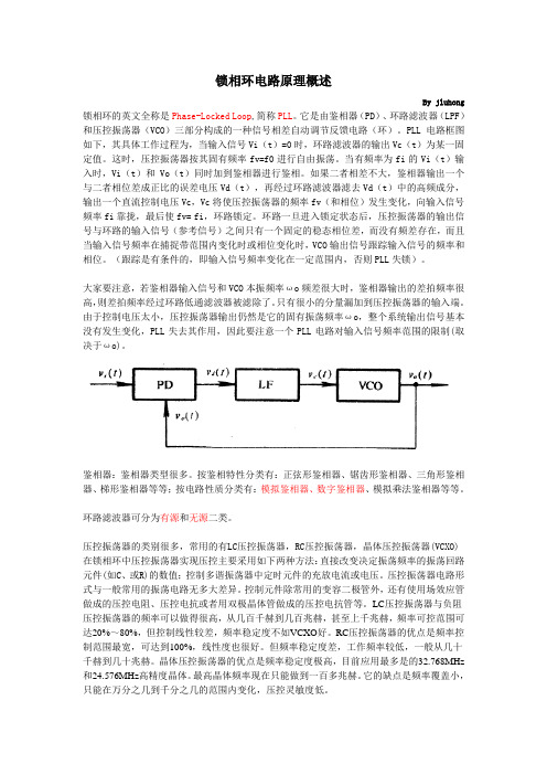
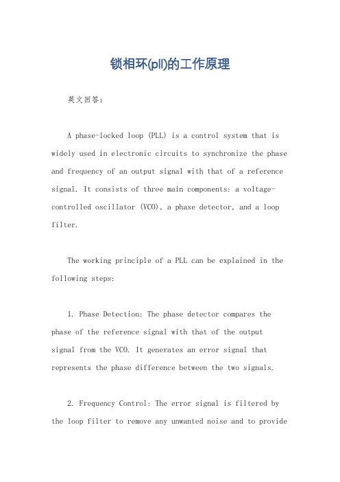
锁相环电路原理概述By jluhong 锁相环的英文全称是Phase-Locked Loop,简称PLL。
它是由鉴相器(PD)、环路滤波器(LPF)和压控振荡器(VCO)三部分构成的一种信号相差自动调节反馈电路(环)。
PLL电路框图如下,其具体工作过程为,当输入信号Vi(t)=0时,环路滤波器的输出Vc(t)为某一固定值。
这时,压控振荡器按其固有频率fv=f0进行自由振荡。
当有频率为fi的Vi(t)输入时,Vi(t)和Vo(t)同时加到鉴相器进行鉴相。
如果二者相差不大,鉴相器输出一个与二者相位差成正比的误差电压Vd(t),再经过环路滤波器滤去Vd(t)中的高频成分,输出一个直流控制电压Vc,Vc将使压控振荡器的频率fv(和相位)发生变化,向输入信号频率fi靠拢,最后使fv= fi,环路锁定。
环路一旦进入锁定状态后,压控振荡器的输出信号与环路的输入信号(参考信号)之间只有一个固定的稳态相位差,而没有频差存在,而且当输入信号频率在捕捉带范围内变化时或相位变化时,VCO输出信号跟踪输入信号的频率和相位。
(跟踪是有条件的,即输入信号频率变化在一定范围内,否则PLL失锁)。
大家要注意,若鉴相器输入信号和VCO本振频率ωo频差很大时,鉴相器输出的差拍频率很高,则差拍频率经过环路低通滤波器被滤除了。
只有很小的分量漏加到压控振荡器的输入端。
由于控制电压太小,压控振荡器输出仍然是它的固有振荡频率ωo,整个系统输出信号基本没有发生变化,PLL失去其作用,因此要注意一个PLL电路对输入信号频率范围的限制(取决于ωo)。
鉴相器:鉴相器类型很多。
按鉴相特性分类有:正弦形鉴相器、锯齿形鉴相器、三角形鉴相器、梯形鉴相器等等;按电路性质分类有:模拟鉴相器、数字鉴相器、模拟乘法鉴相器等等。
环路滤波器可分为有源和无源二类。
压控振荡器的类别很多,常用的有LC压控振荡器,RC压控振荡器,晶体压控振荡器(VCXO)在锁相环中压控振荡器实现压控主要采用如下两种方法:直接改变决定振荡频率的振荡回路元件(如C、或R)的数值;控制多谐振荡器中定时元件的充放电流或电压。
全数字锁相环的VHDL设计【文献综述】
文献综述电子信息工程全数字锁相环的VHDL设计前言锁相环其实不是什么新东西,很早以前就有人使用了。
锁相技术的理论早在1932年就被提出来了,但直到40年代在电视机中才得到广泛的应用,用于改善电视接收机的行同步和帧同步,以提高抗干扰能力。
20世纪50年代后期随着空间技术的发展,锁相环用于对宇宙飞行目标的跟踪、遥测和遥控。
60年代初随着数字通信系统的发展,锁相环应用愈广,例如为相干解调提取参考载波、建立位同步等。
具有门限扩展能力的调频信号锁相鉴频器也是在60年代初发展起来的。
在电子仪器方面,锁相环在频率合成器和相位计等仪器中起了重要作用。
锁相环的英文全称是(Phase-Locked Loop),简称PLL,锁相的意义是相位同步的自动控制,能够完成两个电信号相位同步的自动控制闭环系统叫做锁相环。
是实现相位自动控制的负反馈系统,它使振荡器的相位和频率与输入信号的相位和频率同步。
主题从前言的论述中我们知道了锁相环路具有一些相当优良的功能,且成本低、使用方便,因而它已成为电子技术领域中一种相当有用的技术手段,获得了越来越广泛的应用。
锁相环可以分为模拟锁相环和数字锁相环。
模拟锁相环主要由相位参考提取电路、压控振荡器、相位比较器、控制电路等组成。
压控振荡器输出的是与需要频率很接近的等幅信号,把它和由相位参考提取电路从信号中提取的参考信号同时送入相位比较器,用比较形成的误差通过控制电路使压控振荡器的频率向减小误差绝对值的方向连续变化,实现锁相,从而达到同步。
数字锁相环主要由相位参考提取电路、晶体振荡器、分频器、相位比较器、脉冲补抹门等组成。
分频器输出的信号频率与所需频率十分接近,把它和从信号中提取的相位参考信号同时送入相位比较器,比较结果示出本地频率高了时就通过补抹门抹掉一个输入分频器的脉冲,相当于本地振荡频率降低;相反,若示出本地频率低了时就在分频器输入端的两个输入脉冲间插入一个脉冲,相当于本地振荡频率上升,从而达到同步[1]。
锁相技术译文翻译
锁相技术译文翻译英文原文:An On-Chip All-Digital Measurement Circuit to Characterize Phase-Locked Loop Response in 45-nm SOI译文:45纳米SOI全数字片上测量电路表征锁相环响应特性年级专业:姓名:学号:2013 年 6 月 2 日英文中文An On-Chip All-Digital Measurement Circuit to Characterize Phase-Locked Loop Response in 45-nm SOIAbstract—An all-digital measurement Circuit , built in 45-nm SOI-CMOS enabl es on-chip characterization of phase-loc ked loop (PLL) response to a self-induce d phase step.This technique allows estimationof PLL closed-loop bandwidth and jitterpeaking. The circuit canbe used to plot step-response vs.time, measure static phase error,and observe phase-lock status. INTRODUCTIONMany applications such as PCI Express ? require a PLL to produce alow-jitter cl ock at a given frequency while meeting stringent bandwidth and jitter peaking r 45纳米SOI全数字片上测量电路表征锁相环响应特性摘要---建立在45纳米的SOI-CMOS上一个全数字测量电路,它能够表征PLL对自诱导相步进的响应这项技术允许对PLL闭环带宽和抖动峰值的估计。
司洪珲的外文翻译
本科生毕业设计 (论文)外文翻译原文标题Designing,Simulating,and Testing an AnalogPhase-Locked LoopPhase-Locked Loop in a Digital Environment译文标题在数码环境下设计、模拟和测试一个模拟锁相环作者所在系别电子工程系作者所在专业自动化作者所在班级B06223作者姓名司洪珲作者学号20064022318指导教师姓名齐建玲指导教师职称副教授完成时间2009 年12 月北华航天工业学院教务处制译文标题在数码环境下设计,模拟和测试一个模拟锁相环原文标题Designing,Simulating,and Testing an Analog Phase-Locked Loop in aDigital Environment作者Thomas J. ThatcherMichael M. OshimaCindy Botelho译名托马斯.撒切尔罗切斯特辛迪博特略国籍美国美国美国原文出处April 1997 Hewlett-Packard Journal 6在数码环境下设计,模拟和测试一个模拟锁相环唐静文,中国香港罗切斯特,美国设计用在几项惠普ASIC上的锁相环时,现有阶段的数字部分锁相环被转移成一个VHDL描述与合成的行为。
在模拟部分写出一种行为模型,使ASIC设计师模拟运行系统。
开发出了一种新的非常有效的,用于筛选出在原来的设计过滤过程中的缺陷的泄漏试验。
本文介绍了设计和集成几个正在当前应用专用集成电路的锁相环的一个阶段过程。
该设计是基于锁相环的ASIC上一个循环,但有一些改进。
首先,该阶段的数字部分锁相环被转移到了一种VHDL描述与合成的行为。
在编写代码时,可重用性是一个大的考虑。
VHDL代码的便携性使我们能在很短的时间内设计几种锁相环。
第二,写一个行为模型的模拟部分,这样使ASIC设计师模拟运行系统。
在全数字化设计环境下,对于设计师模拟锁相环提出了若干挑战。
第十五篇 锁相环PLL及APBDIV
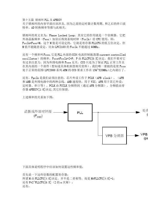
第十五篇锁相环PLL及APBDIV关于锁相环的内容早就应该涉及,因为之前的定时器计数周期,和之后的串口波特率、AD转换频率等都与此相关。
锁相环的英文名为:Phase Locked Loop,其实它的作用就是一个倍频器,它把外部晶振频率(Fosc)加倍后得到系统时钟(Fcclk)给CPU使用,即:Fcclk=Fosc*M,这个M值是可设定的,它就是寄存器PLLCFG的低五位决定,但M值不能随意设定,比如LPC2103的Fcclk不能超过60MHz。
还有一个频率叫Fcco,它是PLL内部的CCO(电流控制振荡器current controlled oscillator)的频率,Fcco=Fcclk*2*P,P由PLLCFG[6:5]决定,我们不要对它有过多注意力,因为外围电路和Fcco无关,CCO只是为了保证PLL正常工作且在其内部的一个部件(想知道具体机制查相关资料),我们唯一要做的是使Fcco 处于正常的范围(LPC2000系列ARM的CCO要求工作在156~320MHz)之内就行了。
还有,Fpclk是我们必须注意的,芯片外设工作于PCLK(APB clock),(APB 和AHB是外围电路中的两种总线,AHB速度快,用于VIC;APB用于其它外设:定时器、串口等),PCLK由FCCLK分频得到(通过APB分频器),分频值由寄存器APBDIV[1:0]决定,其它位保留。
上述频率的关系如下图:下面具体说明程序中应该如何设置这些频率值:首先说一下这些倍数的配置寄存器:所谓M由PLLCFG[4:0]决定,并不是二者相等,而是M=PLLCFG[4:0]+1;还有P=2^PLLCFG[6:5](2的n次幂);还有:APBDIV[1:0]=00,Fcclk/Fpclk=1/4;APBDIV[1:0]=01,Fcclk/Fpclk=1;APBDIV[1:0]=10,Fcclk/Fpclk=1/2;APBDIV[1:0]=11,保留。
锁相环(pll)的工作原理
锁相环(pll)的工作原理英文回答:A phase-locked loop (PLL) is a control system that is widely used in electronic circuits to synchronize the phase and frequency of an output signal with that of a reference signal. It consists of three main components: a voltage-controlled oscillator (VCO), a phase detector, and a loop filter.The working principle of a PLL can be explained in the following steps:1. Phase Detection: The phase detector compares the phase of the reference signal with that of the output signal from the VCO. It generates an error signal that represents the phase difference between the two signals.2. Frequency Control: The error signal is filtered by the loop filter to remove any unwanted noise and to providea smooth control signal. This control signal is then applied to the VCO, which adjusts its frequency based on the control input.3. Phase Comparison: The output signal from the VCO is again compared with the reference signal, and the process of phase detection and frequency control is repeated. This feedback loop continues until the phase difference between the two signals is minimized.4. Locking: Once the phase difference is reduced to zero, the PLL is said to be locked. At this point, the output signal is in sync with the reference signal, and the VCO maintains a stable frequency and phase relationship with the input signal.The PLL can be used in various applications, such as clock synchronization, frequency synthesis, and demodulation. It provides a reliable and accurate methodfor maintaining phase and frequency coherence between different signals.中文回答:锁相环(PLL)是一种广泛应用于电子电路中的控制系统,用于将输出信号的相位和频率与参考信号同步。
锁相技术译文翻译

signal, and the secondary signal is a signal with phase lagofπ/2rad to the fundamental component. The PLL methodsamong them have the potential to correctly estimate the phaseand frequency of frequency-varying single-phase signals.
Index Terms—Frequency estimation, phase estimation, phaselockedloop (PLL), single phase.
I. INTRODUCTION
PHASE, frequency, and amplitude of single-phase voltages
Paper IPCSD-07-073, presented at the 2007 Power Conversion Conference,Nagoya,Japan, April 2–5, and approved for publication in the IEEE TRANSACTIONS ONINDUSTRYAPPLICATIONSby the Industrial Power Converter Committee of the IEEE Industry Applications Society. Manuscript submitted for review April 27, 2007 and released for publication September 6, 2007.
锁相环外文翻译
外文资料Phase-locked loop Technology :A phase-locked loop or phase lock loop (PLL) is a control system that generates a signal that has a fixed relation to the phase of a "reference" signal. A phase-locked loop circuit responds to both the frequency and the phase of the input signals, automatically raising or lowering the frequency of a controlled oscillator until it is matched to the reference in both frequency and phase. A phase-locked loop is an example of a control system using negative feedback. In the order of the PLL is the way of made the frequency stability in the send up wireless,include VCO and PLL integrated circuits,VCO send up a signal,some of the signal is output,and the other through the frequency division with PLL integrated circuits generate the local signal making compared.In the order to remain the same,it’s must be remain the phase displacement same.If the phase displacement have some changes,the output of the PLL integrated circuits have some changes too,to controlle VCO until phase diffe rence to restore,make both cotrolled oscillator’s frequency and phase with input signal which is close-loop electronic circuit keep firm relationship.Phase-locked loops are widely used in radio, telecommunications, computers and other electronic applications. They may generate stable frequencies, recover a signal from a noisy communication channel, or distribute clock timing pulses in digital logic designs such as microprocessors. Since a single integrated circuit can provide a complete phase-locked-loop building block, the technique is widely used in modern electronic devices, with output frequencies from a fraction of a cycle per second up to many gigahertz.Earliest research towards what became known as the phase-locked loop goes back to 1932, when British researchers developed an alternative to Edwin Armstrong's superheterodyne receiver, the Homodyne. In the homodyne or synchrodyne system, a local oscillator was tuned to the desired input frequency and multiplied with the input signal. The resulting output signal included the original audio modulation information.The intent was to develop an alternative receiver circuit that required fewer tuned circuits than the superheterodyne receiver. Since the local oscillator would rapidly drift in frequency, an automatic correction signal was applied to the oscillator, maintaining it in the same phase and frequency as the desired signal. The technique was described in 1932, in a paper by H.de Bellescise, in the French journal Onde Electrique.In analog television receivers since at least the late 1930s, phase-locked-loop horizontal and vertical sweep circuits are locked to synchronization pulses in the broadcast signal. When Signetics introduced a line of monolithic integrated circuits that were complete phase-locked loop systems on a chip in 1969, applications for the technique multiplied. A few years later RCA introduced the "CD4046" CMOS Micropower Phase-Locked Loop, which became a popular integrated circuit. Applications:Phase-locked loops are widely used for synchronization purposes; in space communications for coherent carrier tracking and threshold extension, bit synchronization, and symbol synchronization. Phase-locked loops can also be used to demodulate frequency-modulated signals. In radio transmitters, a PLL is used to synthesize new frequencies which are a multiple of a reference frequency, with the same stability as the reference frequency.Clock recovery :Some data streams, especially high-speed serial data streams (such as the raw stream of data from the magnetic head of a disk drive), are sent without an accompanying clock. The receiver generates a clock from an approximate frequency reference, and then phase-aligns to the transitions in the data stream with a PLL. This process is referred to as clock recovery. In order for this scheme to work, the data stream must have a transition frequently enough to correct any drift in the PLL's oscillator. Typically, some sort of redundant encoding is used; 8B10B is very common.Deskewing :If a clock is sent in parallel with data, that clock can be used to sample the data.Because the clock must be received and amplified before it can drive the flip-flops which sample the data, there will be a finite, and process-, temperature-, and voltage-dependent delay between the detected clock edge and the received data window. This delay limits the frequency at which data can be sent. One way of eliminating this delay is to include a deskew PLL on the receive side, so that the clock at each data flip-flop is phase-matched to the received clock. In that type of application, a special form of a PLL called a Delay-Locked Loop (DLL) is frequently used.Clock generation:Many electronic systems include processors of various sorts that operate at hundreds of megahertz. Typically, the clocks supplied to these processors come from clock generator PLLs, which multiply a lower-frequency reference clock (usually 50 or 100 MHz) up to the operating frequency of the processor. The multiplication factor can be quite large in cases where the operating frequency is multiple gigahertz and the reference crystal is just tens or hundreds of megahertz.Spread spectrum:All electronic systems emit some unwanted radio frequency energy. Various regulatory agencies (such as the FCC in the United States) put limits on the emitted energy and any interference caused by it. The emitted noise generally appears at sharp spectral peaks (usually at the operating frequency of the device, and a few harmonics).A system designer can use a spread-spectrum PLL to reduce interference with high-Q receivers by spreading the energy over a larger portion of the spectrum. For example, by changing the operating frequency up and down by a small amount (about 1%), a device running at hundreds of megahertz can spread its interference evenly over a few megahertz of spectrum, which drastically reduces the amount of noise seen by FM receivers which have a bandwidth of tens of kilohertz.中文翻译锁相环技术:锁相环或锁相回路(PLL)是一个信号控制系统,即用来锁定一系列的“参考”信号。
锁相环
锁相环的英文全称是Phase-Locked Loop,简称PLL。
锁相环电路是一种反馈电路,其作用是使得电路上的时钟和某一外部时钟的相位同步。
因锁相环可以实现输出信号频率对输入信号频率的自动跟踪,所以锁相环通常用于闭环跟踪电路。
锁相环在工作的过程中,当输出信号的频率与输入信号的频率相等时,输出电压与输入电压保持固定的相位差值,即输出电压与输入电压的相位被锁住,这就是锁相环名称的由来。
锁相环的工作原理:1. 压控振荡器的输出经过采集并分频;2. 和基准信号同时输入鉴相器; 3. 鉴相器通过比较上述两个信号的频率差,然后输出一个直流脉冲电压;4. 控制VCO,使它的频率改变;5. 这样经过一个很短的时间,VCO 的输出就会稳定于某一期望值。
锁相环路在锁定后,不仅能使输出信号频率与输入信号频率严格同步,而且还具有频率跟踪特性,所以它在电子技术的各个领域中都有着广泛的应用。
PLL实际上是一负反馈系统,只要输入信号在正常范围内,输出信号在“一定时间内”都能跟上。
输入信号发生变化后,输出信号跟踪输入信号的过程称之为捕获;输出信号跟踪完毕时称之为锁定;输入信号变化过快导致输出信号无法跟踪时称为失锁。
在数据采集系统中,锁相环是一种非常有用的同步技术,因为通过锁相环,可以使得不同的数据采集板卡共享同一个采样时钟。
因此,所有板卡上各自的本地80MHz 和20MHz时基的相位都是同步的,从而采样时钟也是同步的。
因为每块板卡的采样时钟都是同步的,所以都能严格地在同一时刻进行数据采集。
PLL通常由鉴相器(PD)、环路滤波器(LF)和压控振荡器(VCO)三部分组成,PLL组成的原理框图如图1所示。
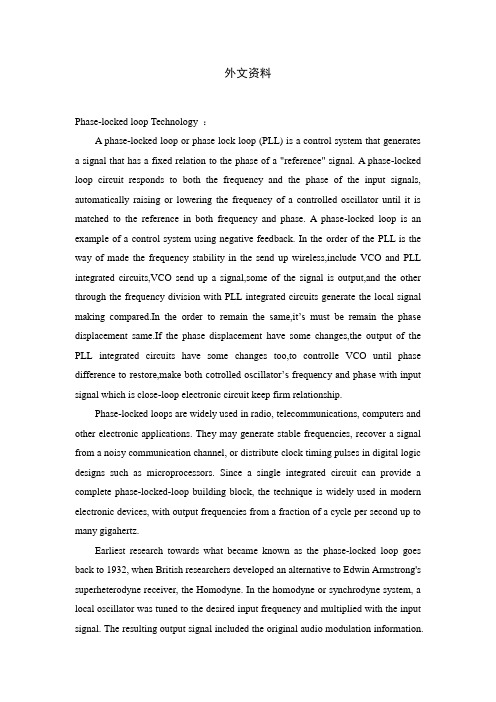
如图2所示,PLL频率合成器是由参考频率源、参考分频器、相位比较器、环路滤波器、压控振荡器、可变分频器构成。
参考分频器对参考频率源进行分频,输出信号作为相位比较器参考信号。
可变分频器对压控振荡器的输出信号进行分频,分频之后返回到相位比较器输入端与参考信号进行比较。
集成电路器件的中英文英文名称对照
(4)译码器(decoder)
(5) 数据比较器(comparator)
(6) 驱动器(driver)
(7) 计数器(counter)
(8) 整形电路
(9)可编程逻辑器件(PLD)
(10) 微处理器(microprocessor,MPU)
(11)单片机(Microcontroller,MCU)
器件的英文名称
(1)集成运算放大器(operation amplifier),简称集成运放
(2) 比较器(comparator)
(3)对数和指数放大器
(4) 模拟乘/除法器(multiplier/divider)
(5) 模拟开关电路(analog switch)
(6) PLL电路(phase lock loop),即锁相环电路
(7)集成稳压器(voltage regulatoБайду номын сангаас)
(8) 参考电源(reference source)
(9)波形发生器(wave-form generator)
(10)功率放大器(power amplifier)
3.数字集成电路器件
(1) 基本逻辑门(logic gate circuit)
(2) 触发器(flip-flop)
(12) DSP器件(Digital signal processor,DSP)
集成运算放大器operationamplifier简称集成运放模拟开关电路analogswitchpll电路phaselockloop即锁相环电路集成稳压器voltageregulator参考电源referencesource波形发生器waveformgenerator10功率放大器poweramplifier基本逻辑门logicgatecircuit可编程逻辑器件pld10微处理器microprocessormpu11单片机microcontrollermcu12dsp器件digitalsignalprocessordsp
锁相技术译文翻译:数字混合PLL频率合成器的开关特性分析
At first,C1andR1are considered for a second-order PLL system design to meet the desired specifications withoutC2.
Index Terms—Device error and switching, digital hybrid phase-locked loop (DH-PLL), frequency synthesizer.
I. INTRODUCTION
HIGH-SPEED switching is one of the most important characteristics in frequency synthesizers. In 1999, Abou El-Ela proposed a method in which an additional input to a voltage control oscillator (VCO) is required to get higher switching speed in a phase-locked loop (PLL) frequency synthesizer [1]. This is a structure to provide VCO with an additional input of the sawtooth wave using a digital-to-analog (D/A) converter. Whenever frequency is synthesized, the waveform generator with the most optimum slope and duration is required. Therefore, the complicated design and the exact synchronization for high-speed switching make it disadvantageous.In 1995, Materna addressed the PLL structure based on a pre-tuning approach that uses an external tuning voltage to a VCO by a D/A converter for extremely high-frequency satellite applications [2]. However, there was no discussion about the system switching characteristics. In 2001,Ryuproposed a simplified structure that improves switching speed and power consumption of the digital direct-frequency synthesizer (DDFS)-driven PLL [3]. Although there is an advantage of the effective wide-band applications, the operating speed of the whole system depends on PLL speed. In 2000, Fouzar proposed a PLL frequency synthesizer that has dual-loop form using a frequency-to-voltageconverter (FVC) [4]. High switching speed can be obtained by use of the FVC and the coarse tuning controller using the output of the phase detector and VCO. Additional hardware complexity is cumbersome and FVC limits the switching speed.
外文翻译--相位锁相环
外文翻译--相位锁相环外文翻译■ THE PHASE-LOCKED LOOP PLLThe PLL as an FM DemodulatorAs you have seen the VCO control voltage in a PLL depends on the deviation of the incoming frequency The PLL will produce a voltage proportional to the frequency of the incoming signal which in the case of FM is the original modulating signalFigure 13-54 shows a typical connection for the LM565 as an FM demodulator If the IF input is frequency modulated by a sinusoidal signal you get a sinusoidal signal on the output as indicated Since the imum operating frequency is 500 kHz this device must be used in double-conversion FM receiver is one in which essentially two mixers are used to first convert the RF to a 107 MHz IF and then convert this to a 455 kHz IFThe free-running frequency of the VCO is adjusted to approximately 455 kHz which is the center of the modulated IF range C can be any value but R should be in the range from 2kΩ to 20kΩ The input van be directly coupled as long as there is no dc voltage difference between pins 2 and 3The VCO is connected to the phase detector by an external wire betweenpins 4 and 5Determine the values for RC and C for the LM565 in Figure 13-54 for a free-running frequency of 455 kHz and a capture range of ±10kHzThe dc supply voltages are ± 6VSolution Use Equation 13-5 to calculate CChoose R 47kΩ■ COMMUNICATIONS CIRCUITSThe lock range and capture range must be determined before C can be calculated The lock range isUse Equation 13-7 to calculate CThereforePractice Exercise What can you do to increase the capture range from ±10 kHz to ± 15 kHz13-8 REVIEW QUESTIONS1 List the three basic components in a phase-locked loop2 What is another circuit used in some PLLs other than the three listed in Question 13 What is the basic function of a PLL4 What is the difference between the lock range and the capture range lf a PLL5 Basically how does a PLL track the incoming frequency■ A SYSTEM APPLICATIONThe DCE data communications equipment system introduced at the opening of this chapter includes an FSK frequency shift keying modem modulatordemodulator FSK is one method for modulating digital data for transmission over voice phone lines and is basically a form of frequency modulation In this system application the focus is on the low-speed modulatordemodulator modem board which is implemented with a VCO for transmitting FSK signals and a PLL for receiving FSK signalsAfter completing this section you should be able toApply what you have learned in this chapter to a system applicationDescribe how a VCO and a PLL can be used in a communications system Discuss how FSK is used to send digital information over phone lines Translate between a printed circuit board and a schematicAnalyze the modem circuitryTroubleshoot some common problems■ A SYSTEM APPLICATIONA Brief Description of the SystemThe FSK modem interfaces a computer with the telephone network so that digital data which are incompatible with the standard phone system because of bandwidth limitations can be transmitted and received over regular phone lines thus allowing computers to communicate with each other Figure13-55 shows a diagram of a simple data communications system in which a modem at each end of the phone line provides interfacing for a computerA data communications systemThe modem DCE consists of three basic functional blocks as shown in Figure 13-56the FSK modem circuits the phone line interface circuits and the timing and control circuits The dual polarity power supply is not shown Although the focus lf this system application is the FSK modem board we will briefly look at each of the other parts to give you a basic idea of the overall system functionBasic block diagram of a modem■ COMMUNICATIONS CIRCUITSThe Phone Line Interface The main purposes of this circuitry are to couple the phone line to the modem by proper impedance matching to provide necessary filtering and to accommodate full-duplex transmission of data Full-duplex means essentially that information can be going both ways on a single phone line at the same time This allows a computer connected to a modem to be sending data and receiving data simultaneously without the transmitted data interfering with the received data Full-duplexing is implemented by assigning the transmitted data one bandwidth and the received data another separate bandwidth within the 300 Hz to 3 kHz overall bandwidth of the phone networkTiming and Control One basic function of the timing and controlcircuits is to determine the proper mode of operation for the modem The two modes are the originate mode and the answer mode Another function is to provide a standard interface such as RS-232C with the DTE computer The RS-232C standard requires certain defined command and control signals data signals and voltage levels for each signalDigital Data Before we get into FSK lets briefly review digital data A detailed knowledge of binary numbers is not necessary for this system application Information is represented in digital form by 1s and 0s which are the binary digits or bits In terms of voltage waveforms a 1 is generally represented by a high level and a 0 by a low level A stream of serial data consists if a sequence of bits as illustrated by an example in Figure 13-57 aFIGURE 13-57A serial stream of digital dataBaud Rate A low-speed modem such as the one we are focusing on sends and receives digital data at a rate of 300 bitss or 300 baud5For example if we have an alternating sequence of 1s and 0s highs and lows as indicated in Figure 13-57 b each bit takes 333 ms Since it takes two bits a 1 and a 0 to make up the period of this particular waveform the fundamental frequency of this format is 1667 ms 150 Hz This is the imum frequency of a 300 baud data stream because normally there may be several consecutive 1s andor several consecutive zeros in a sequence thus reducingthe frequency As mentioned earlier the telephone network has a 300 Hz minimum frequency response so the fundamental frequency of the 300 baud data stream will fall outside of the telephone bandwidth This prevents sending digital data in its pure form over the phone lines Technically bit rate and baud rate are not the same Baud rate indicates how many frequency shifts are sent per second Each frequency shift can represent more than one bit thus a 14400 bitss modem actually transmits at 2400 baud■ SYSTEM APPLICATIONFrequency-Shift Keying FSK FSK is one method used to overcome the bandwidth limitation of the telephone so that digital data can be sent over the phone lines The basic idea of FSK is to represent 1s and 0s by two different frequencies within the telephone bandwidth By the way any frequency within the telephone bandwidth is an audible tone The standard frequencies for a full-duplex 300 baud modem in the originate mode are 1070 Hz for a 0 called a space and 1270 Hz for a 1 called a mark In the answer mode 2025 Hz is a 0 and 2225 Hz is a 1 The relationship of these FSK frequencies and the telephone bandwidth is illustrated in Figure 13-58Signals in both the originate and answer bands can exist at the same time on the phone line and not interfere with each other because of the frequency separationFrequencies for 300 baud full-duplex data transmissionAn example of a digital data stream converted to FSK by a modem is shown in FigureExample if FSK data■ COMMUNICATIONS CIRCUITSModem Circuit OperationThe FSK modem circuits shown in Figure 13-60 contain an LM565 PLL and a VCO integrated circuit The VCO can be a device such as the 4046 not covered specifically in this chapter which is a PLL device in which the VCO portion van be used by itself because all of the necessary inputs and outputs are available The VCO in the LM565cannot be used independently of the PLL because there is on input pin for the control voltage The function of the VCO is to accept digital data from a DTE and provide FSK modulation The VCO is always the transmitting device The digital data come in on the control voltage input pin 9 of the VCO via a level-shifting circuit formed by Q3 and Q4This circuit is used because the data from the RS-232C interface are dual polarity with a positive voltage representing a 0 and a negative voltage representing a 1Potentiometer R8 is for adjusting the high level of the control voltage and R11 is for adjusting the low level for the purpose of fine-tuning the frequency Transistor Q5 provides for originateanswer mode frequency selection by changing the value of the frequency-selection resistance from pin 11 to ground Transistors Q1 and Q2 perform a similar functionfor the PLL■ A SYSTEM APPLICATIONWhen the digital data are at high levels corresponding to logic 0s the VCO oscillates at 1070 Hz in the originate mode and 2025 Hz in the answer mode When the digital data are at low levels corresponding to logic 1s the VCO oscillates at 1270 Hz in the originate mode and 2225 Hz in the answer mode An example of the originate mode is when the receiving DTE responds to a request and sends data back to the originating DTE The function of the PLL is to accept incoming FSK-modulated data and convert it to a digital data format for use by the DTD The PLL is always a receiving device When the modem is in the originate mode the PLL os receiving originate-mode data from the other modem The 741 op-amp is connected as a comparator that changes the data levels from the PLL to dual-polarity format for compatibility with the RS-232C interface Now so that you can take a closer look at the FSK modem board lets take it out of the system and put it on the troubleshooters bench TROUBLESHOOTERS BENCH■ ACTIVITY 1 Relate the PC Board to the SchematicLocate and identify each component and each inputoutput pin on the PC board in Figure 13-61 using the schematic in Figure 13-60 Verify that the board and the schematic agree If the PC board and the schematic do not agree indicate the problem■ COMMUNICATIONS CIRCUITS■ ACTIVITY 2 Analyze the CIRCUITSFor this application the free-running frequencies of both the PLL and the VCO circuits are determined by the formula in Equation 13-5 Step 1 Verify that the free-running frequency for the PLL OC is approximately 1070 Hz in the originate mode and approximately 1270 Hz in the answer modeStep 2 repeat Step 1 for the VCOStep 3 Determine the approximate minimum and imum output voltages for the 741 comparatorStep 4 Determine the imum high-level voltage on pin 9 of the VCO Step 5 If a 300 Hz square wave that varies from 5 V to –5 V is applied to the data from the DTE input what should you observe on pin 4 of the VCOStep 6 When the data from the DTE are low pin 9 of the VCO is at approximately 0V At this level the VCO oscillates at 1070 Hz or 2025 Hz When the data from the DTE go high to what value should the voltage at pin 9 be adjusted to produce a 1270 Hz or 2225 Hz frequency if the transfer function of the VCO is 50 HzV■ ACTIVITY 3 Write a Technical ReportDescribe the overall operation of the FSK modem board Specify how each circuit works and what its purpose is Identify the function of eachcomponent Use the results of Activity 2 as appropriate■ ACTIVITY 4 Troubleshoot the System for Each of the Following Problems By Stating the probable Cause or Causes1 There is no demodulated data output voltage when there are verified FSK data from the phone line interface2 The LM565 properly demodulates 1070 Hz and 1270 Hz FSK data but does not properly demodulate 2025 Hz and 2225 Hz data3 The VCO produces no FSK output4 The VCO produces a continuous 1070 Hz tone in the originate mode and a continuous 2025 Hz tone in the answer mode when there are proper data from the DTE13-9 REVIEW QUESTIONS1 The originateanswer input to the modem is low In what mode is the system2 What is the purpose of diode D1 in the FSK modem circuit3 The VCO is transmitting 1070 Hz and 1270 Hz FSK signals To what frequencies does the PLL respond from another modem4 If the VCO is transmitting a constant 2225 Hz tone what does this correspond to in terms of digital data I what mode is the modem ■ GLOSSARY■SUMMARY ■In amplitude modulation AM the amplitude of a higher-frequency carrier signal is varied by a lower–frequencymodulating signal usually an audio signal■A basic superheterodyne AM receiver consists of an RF amplifier not always a mixer a local oscillator an IF intermediate frequency amplifier an AM detector and audio and power amplifiers■The IF in a standard AM receiver is 455 kHz■The AGC automatic gain control in a receiver tends to keep the signal strength constant within the receiver to compensate for variations in the received signal■In frequency modulation FM the frequency of a carrier signal is varied by a modulating signal A superheterodyne FM receiver is basically the same as an AM receiver except that it requires a limiter to keep the IF amplitude constant a different kind of detector or discriminator and a de-emphasis network The IF is 107 MHz■A four-quadrant linear multiplier can handle any combination of voltage polarities on its inputs■Amplitude modulation is basically a multiplication process■The multiplication of sinusoidal signals produces sum and difference frequencies■The output spectrum of a balanced modulator includes upper-side and lower-side frequencies but no carrier frequency■The output spectrum of a standard amplitude modulator includes upper-side and lower-side frequencies and the carrier frequency■A linear multiplier is used as the mixer in receiver systems■A mixer converts the RF signal down to the IF signal The radio frequency varies over the AM or FM band The intermediate frequency is constant■One type of AM demodulator consists of a multiplier followed by a low-pass filter■The audio and power amplifiers boost the output of the detector or discriminator and drive the speaker■A voltage-controlled oscillator VCO produces an output frequency that can be varied bb a control voltage Its operation is based on a variable reactance■A VCO is a basic frequency modulator when the modulating signal is applied to the control voltage input■A phase-locked loop PLL is a feedback circuit consisting of a phase detector a low-pass filter a VCO and sometimes an amplifier ■The purpose of a PLL is to lock onto and track incoming frequencies ■A linear multiplier can be used as a phase detector■A modem is a modulatordemodulator■DTE stands for digital terminal equipment■DCE stands for digital communications equipment■ GLOSSARY Key terms are in color All terms are included in the end-of-book glossaryAmplitude modulation AM A communication method in which a lower-frequency signal modulates varies the amplitude of a higher-frequency signal carrierAudio Related to the range of frequencies that can be heard by the human ear and generally considered to be in the 20 Hz to 20 kHz range Balanced modulation A form of amplitude modulation in which the carrier is suppressed sometimes known as suppressed-carrier modulation Demodulation The process in which the information signal is recovered from the IF carrier signal the reverse of modulation ■ COMMUNICATIONS CIRCUITSDiscriminator A type of FM demodulatorFour-quadrant multiplier A linear device that produces an output voltage proportional to the product of two input voltages Frequency modulation FM A communication method in which a lower-frequency intelligence-carrying signal modulates varies the frequency of a higher-frequency signalMixer A device for down-converting frequencies in a receiver system Modem A device that converts signals produced by one type of device to a form compatible with another modulatordemodulatorModulation The process in which a signal containing information is used to modify the amplitude frequency or phase of a much higher-frequency signal called the carrierPhase-locked loop PLL A device for locking onto and tracking the frequency of an incoming signalVoltage-controlled oscillator VCO An oscillator for which the output frequency is dependent on a controlling input voltage ■ KEY 13-1 Multiplier output voltageFORMULAS13-2 Sum and difference frequencies13-3 Standard AM13-4 PLL control voltage13-5 Output frequency LM56513-6 Lock range LM56513-7 Capture range LM565■SELF-TEST Answers are at the end of the chapter1 In amplitude modulation the pattern produced by the peaks of the carrier signal is called theindex envelope audio signal upper-side frequency2 Which of the following is not a part of an AM superheterodyne receiverMixer IF amplifier DC restorerDetector Audio amplifier Local oscillatorThe power factor of a circuit therefore is the ratio of the averagepowerto the apparentpower For a purely resistive circuit we haveIn general power equipment is rated in volt-amperes VA or in kilovolt-amperes kVA and not in watts By knowing the volt-ampere ratingand the rated voltage of a device we can readily determine the imumcurrent rating For example a device rated at 10 kVA at 200 Vhas a imum current rating of I 10000 VA200 V 50 A whenoperated under rated conditions The volt-ampere rating of a piece ofequipment is equal to the wattage rating only when the Fp is 1 It is herefore a imum power dissipation rating This condition exists nly when the total impedance of a system Z v is such that v 0°The exact current demand of a device when used under normaloperating conditions could be determined if the wattage rating andpower factor were given instead of the volt-ampere rating However thepower factor is sometimes not available or it may vary with the loadb Sketch the power trianglec Find the energy dissipated by the resistor over one full cycle of the iut voltage if the frequency of the input quantities is 60 Hzd Find the energy stored in or returned by the capacitor or inductorover one half-cycle of the power curve for each if the frequency ofhe input quantities is 60 HzFIG 1919Example 192Thus the power factor of the load dropped to 233 kW388 kVA 06whichwould put an unnecessary additional load on the power plant It s certainly time to consider the power-factor-correction option as escribed in this text It is not uncommon to see large capacitors sitting t the point where power enters a large industrial plant to perform aneeded level of power-factor correctionAll in all therefore it is important to fully understand the impact of poor power factor on a power plantwhether you someday work for he supplier or for the consumer1912 COMPUTER ANALYSISPower Curve Resistor The computer analysis will begin with averification of the curves of Fig 193 which show the in-phase relationshipbetween the voltage and current of a resistor The figure shows that he power curve is totally above the horizontal axis and that the curve has a frequency twice the applied frequency and a peak value equal toice the average value First the simple schematic of Fig 1936 musare typically available for tranges Each is fundamentally an independent control that isa change in one can be made without affecting the other two For theparametric equalizer of Fig 2041 each of the six channels has a frequencycontrol switch which in conjunction with the f 10 switch willgive a range of center frequencies from 40 Hz through 16 kHz It hascontrols for BW Q from 3 octaves to 120 octave and 18 dB cut andboostSome like to refer to the parametric equalizer as a sophisticatedtone control and will actually use them to enrich the sound after the flatresponse has been established by the graphic equalizer The effectchieved with a standard tone control knob is sometimes referred to asboring compared to the effect established by a good parametric equalizerprimarily because the former can control only the volume and nothe bandwidth or center frequency In general graphic equalizers establishhe important flat response while parametric equalizers are adjustedto provide the type and quality of sound you like to hear You cannotch out the frequencies that bother you and remove tape hiss andthe sharpness often associated with CDsOne characteristic of concert halls that is more difficult to fake is theullness of sound that concert halls are able to provide In the concerthall you have the direct sound from the instruments and the reflectionof sound off the walls and the vaulted ceilings which were all carefullydesigned expressly for this purpose Any reflection results in a delay inhe sound waves reaching the ear creating the fullness effect Throughdigital delay speakers can be placed to the back and side of a listenerto establish the surround sound effect In general the delay speakers aremuch lower in wattage with 20-W speakers typically used with a 100-Wsystem The echo response is one reason that people often like to playheir stereos louder than they should for normal hearing By playingthestereo louder they create more echo and reflection off the walls bringinginto play some of thfullness heard at concert hallsIt is probably safe to say that any system composed of quality componentsa graphic and parametric equalizer and surround sound willhave all the components necessary to have a quality reproduction of theconcert hall effect 2014 COMPUTER ANALYSISPSpiceSeries Resonance This chapter provides an excellent opportunityto demonstrate what computer software programs can do for us Imaginehaving to plot a detailed resonance curve with all the calculationsrequired for each frequency At every frequency the reactance of theinductive and capacitive elements changes and the phasor operationswould have to be repeateda long and arduous task However withPSpice taking a few moments to enter the circuit and establish thedesired simulation will result in a detailed plot in a few seconds that canhave plot points every microsecondFor the first time the horizontal axis will be in the frequency domainrather than in the time domain as in all the previous plots For the seriesresonant circuit of Fig 2042 the magnitude of the source was chosento produce a imum current of I 400 mV4010 mA at resonanceand the reactive elements will establish a resonant frequencyTechnically bit rate and baud rate are not the same Baud rate indicates how many frequency shifts are sent per second Each frequency shift canrepresent more than one bit thus a 14400 bitss modem actually transmits at 2400 baudWe found the areas under the curves in the preceding example by using a simple geometric formula If we should encounter a sine wave or any other unusual shape however we must find the area by some other means We can obtain a good approximation of the area by attempting to reproduce the original wave shape using a number of small rectangles or other familiar shapes the area of which we already know through simple geometric formulas For examplethe area of the positive or negative pulse of a sine wave is 2Am Approximating this waveform by two triangles Fig 1343 we obtain using area 12 base height for the area of a triangle a rough idea of the actual areaA closer approximation might be a rectangle with two similar triangles Fig 1344which is certainly close to the actual area If an infinite number of forms were used an exact answer of 2Am could be obtained For irregular waveforms this method can be especially useful if data such as the average value are desired The procedure of calculus that gives the exact solution 2Am is known as integration Integration is presented here only to make the method recognizable to the reader it is not necessary to be proficient in its use to continue with this text It is a useful mathematical toolhoweverand should be learned Finding the area under the positive pulse of a sine wave using integration we havewhere ∫is the sign of integration 0 and p are the limits of integration Am sin a is the function to be integrated and da indicates that we are integrating with respect to a Integrating we obtain Since we know the area under the positive or negative pulse we can easily determine the average value of the positive or negative region of a sine wave pulse by applying Eq 1326For the waveform of Fig 1345EXAMPLE 1315 Determine the average value of the sinusoidal waveform of Fig 1346Solution By inspection it is fairly obvious thatthe average value of a pure sinusoidal waveform over one full cycle iszeroEXAMPLE 1316 Determine the average value of the waveform of Fig 1347 Solution The peak-to-peak value of the sinusoidal function is16 mV 2 mV 18 mV The peak amplitude of the sinusoidal waveform is therefore 18 mV2 9 mV Counting down 9 mV from 2 mV or 9 mV up from -16 mV results in an average or dc level of -7 mVas noted by the dashed line of Fig 1347 EXAMPLE 1317 Determine the average value of the waveform of Fig 1348 SolutionEXAMPLE 1318 For the waveform of Fig 1349 determine whether the average value is positive or negative and determine its approximate value Solution From the appearance of the waveform the average value is positive and in the vicinity of 2 mV Occasionally judgments of this type will have to be madeInstrumentationThe dc level or average value of any waveform can be found using a digital multimeter DMM or an oscilloscope For purely dc circuitssimply set the DMM on dc and read the voltage or current levelsOscilloscopes are limited to voltage levels using the sequence of steps listed below1 First choose GND from the DC-GND-AC option list associated with each vertical channel The GND option blocks any signal to which the oscilloscope probe may be connected from entering the oscilloscope and responds with just a horizontal line Set the resulting line in the middle of the vertical axis on the horizontal axis as shown in Fig 1350 a2 Apply the oscilloscope probe to the voltage to be measured if not already connected and switch to the DC option If a dc voltage is present the horizontal line will shift up or down as demonstrated in Fig 1350 b Multiplying the shift by the vertical sensitivity will result in the dc voltage An upward shift is a positive voltage higher potential at the red or positive lead of the oscilloscope while a downward shift is a negative voltage lower potential at the red or positive lead of theoscilloscope In general1 Using the GND option reset the horizontal line to the middle of the screen2 Switch to AC all dc components of the signal to which the probe is connected will be blocked from entering the oscilloscope only the alternating or changing components will be displayedNote the location of some definitive point on the waveform such as the bottom of the half-wave rectified waveform of Fig 1351 a that is note its position on the vertical scale For the future whenever you use the AC option keep in mind that the computer will distribute the waveform above and below the horizontal axis such that the average value is zero that is the area above the axis will equal the area below3 Then switch to DC to permit both the dc and the ac components of the waveform to enter the oscilloscope and note the shift in the chosen level of part 2 as shown in Fig 1351 b Equation1329 can then be used to determine the dc or average value of the waveform For the waveform of Fig 1351 b the average value is about The procedure outlined above can be applied to any alternating waveform such as the one in Fig 1349 In some cases the average value may require moving the starting position of the waveform under the AC option to a different region of the screen or choosing a higher voltage scale DMMs can read the average or dc level of any waveform by simply choosing。
锁相环PLL
锁相环的工作原理与应用
锁相技术的理论早在1932年就提出了,但直到40年代在电视机中才得到广泛的应用。锁相环的英文全称是Phase-Locked Loop,简称PLL,是实现相位自动控制的负反馈系统,它使振荡器的相位和频率与输入信号的相位和频率同步。
锁相环包含三个主要的部分:⑴鉴相环(或单元,用来比较输入信号和基准信号的之间的相位.它的输出电压正比于两个输入信号之相位差.⑵低通滤波器(LPF):是个线性电路,其作用是滤除鉴相器输出电压中的高频分量,起平滑滤波的作用.通常由电阻、电容或电感等组成,有时也包含运算放大器。⑶压控振荡器(VCO):振荡频率受控制电压控制的振荡器,而振荡频率与控制电压之间成线性关系。在PLL中,压控振荡器实际上是把控制电压转换为相位。
中心频率发生偏移。这个偏移方向恰好是朝着输入信号频率Wi的方向移动,使相位比较器输出的差拍信号频率变得越来越低,相位差的直流分量也会越来越大。这个逐渐变大的直流分量经低通滤波器后去控制VCO,以更快的速度使VCO的振荡频率趋向于Wi。 上述过程以极快的速度反复循环进行,直至从量变发生质变:VCO的振荡频率由原来的Wo变为Wi,环路在这个频率上稳定下来,这时相位比较器的输出也由差拍波变为直流电压,环路进入锁定状态。这种锁定状态是环路通过频率的逐步牵引而进入的,这个过程叫做捕捉过程。若Wo与Wi的频差太大,环路通过频率的逐步牵引也可能始终进入不了锁定状态,就称处于失锁状态。这是因为Wo与Wi相差很大时,相位比较器输出的差拍电压的频率很高,它将被低通滤波器除掉,滤波器的输出电压基本上为0或保持不变,因此VCO的输出频率也保持Wo不变,这种情况将一直持续下去。
- 1、下载文档前请自行甄别文档内容的完整性,平台不提供额外的编辑、内容补充、找答案等附加服务。
- 2、"仅部分预览"的文档,不可在线预览部分如存在完整性等问题,可反馈申请退款(可完整预览的文档不适用该条件!)。
- 3、如文档侵犯您的权益,请联系客服反馈,我们会尽快为您处理(人工客服工作时间:9:00-18:30)。
锁相技术译文翻译
英文原名:High Speed Digital Hybrid PLL Frequency Synthesizer
译文:高速数字混合锁相环频率合成器
年纪专业:08级通信工程班
姓名:学号:
2011年 5月2日
To get the high-speed, it is necessary to prepare the precise synchronization of the complicated design.
In 2001, H. G. Ryu proposed a simplified structure of the DDFS (direct digital frequency synthesizer)-driven PLL for the high switching speed [2].
However, there is a problem that the speed of the whole system is limited by PLL.
Y. Fouzar proposed a PLL frequency synthesizer of dual loop configuration using frequency-to-voltage converter (FVC) [3].
It has a fast switching speed by the PD (phase detector), FVC using output signal of VCO and the proposed coarse tuning controller.
However, H/W complexity is increased for the high switching speed.
Also, it shows the fast switching characteristic only when the FVC works well.
Another method is pre-tuning one which is called DH-PLL in this study [4].
It has very high speed switching property, but H/W complexity and power consumption are increased due to digital look-up table (DLT) which is usually implemented by the ROM including the transfer characteristic of
VCO(voltage controlled oscillator).
For this reason, this paper proposes a timing synchronization circuit for the rapid frequency synthesis and a very simple DLT replacement digital logic block instead of the complex ROM type DLT for high speed switching and low power consumption. Also, the requisite condition is solved in the proposed method. The fast switching operation at every the frequency synthesis process is verified by the computer circuit simulation.
II.DH-PLL synthesizer
As shown in Fig.1, the open-loop synthesizer is a direct frequency synthesis type that VCO 要得到高运行速度,事先做好复杂设计的精确同步是必要的。
2001年,H.G.Ryu提出了一种简化结构的直接数字频率合成器(DDFS)驱动的高转换速度锁相环【2】。
但是,有一个问题,整个系统的速度是受锁相环限制的。
Y.Fouzar提出了一种使用频率—电压转换器(FVC)具有双重回路结构的锁相环频率合成器【3】。
因为鉴相器(PD), FVC利用了压控振荡器的输出信号和我们提出的粗调控制器,所以它具有快速切换速度。
但是,因为有高速系统转换速度使得H / W的复杂性增加了。
另外,结果表明只有FVC工作状态良好时系统才有较高切换速度。
另一种方法是做预先调整也就是本项研究中的DH-PLL 【4】。
它具有高速切换的特性,但是因为数字查找表(DLT)的原因,H / W复杂度和功耗明显增大了,因为DLT 经常被ROM执行,DLT中包含压控振荡器(VCO)的传输特性。
介于以上原因, 为得到较高切换速度和低功耗,本文提出了一种新的快速定时同步频率合成电路,用一个非常简单的DLT替代数字逻辑块,而不用复杂的ROM型(DLT)。
同时,在该方法中所需必要条件也解决了,频率合成过程的高切换速度在计算机电路仿真中已经得到验证了。
2.DH-PLL合成器
图1中所示的开环频率合成技术是一种直接频率合成方式,在频率控
desired VCO frequency.
③is fixed until a new FCW is made.
Fig. 4. Operating signal of DH-PLL. 关系是固定的。
图4 DH-PLL工作信号
Fig.5. Block diagram of the new proposed 图5 新提出的DH-PLL框图。
表1 仿真参数。