RailClamp Low Capacitance TVS Diode Array
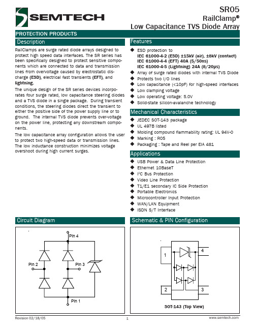
SR05.TCT中文资料

Forward Voltage vs. Forward Current
10 9
% Change in Capacitance 0 -2 -4 -6 -8 -10 -12 -14 -16
Capacitance vs. Reverse Voltage
Forward Voltage - V F (V)
8 7 6 5 4 3 2 1 0 0 5 10 15 20 25 30 35 40 45 50 Forward Current - IF (A) Waveform Parameters: tr = 8µs td = 20µs
SR05
Mechanical Characteristics
JEDEC SOT-143 package UL 497B listed Molding compound flammability rating: UL 94V-0 Marking : R05 Packaging : Tape and Reel per EIA 481
0
25
50
75
100
125
150
Ambient Temperature - TA (oC)
Pulse Waveform
110 100 90 80 Percent of IPP 70 60 50 40 30 20 10 0 0 5 10 15 Time (µs) 20 25 30 td = IPP/2 e
10 Peak Pulse Power - PPk (kW)
Power Derating Curve
1IP 90 80 70 60 50 40 30 20 10 0
1
0.1
RClamp0504S.TCT中文资料
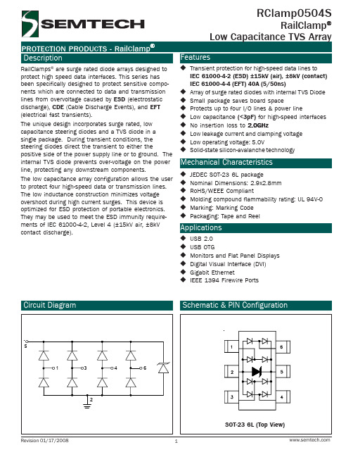
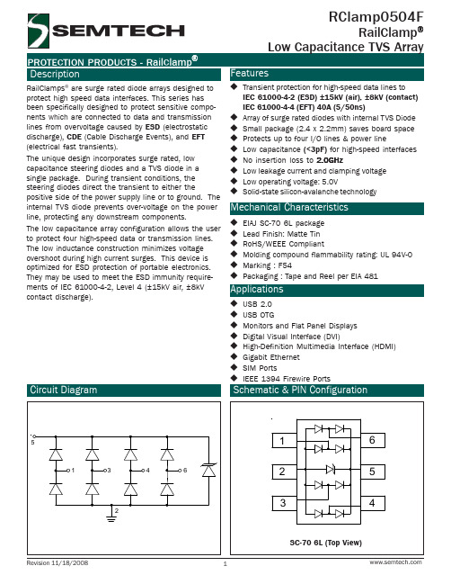
RailClamps are surge rated diode arrays designed to protect high speed data interfaces. This series has been specifically designed to protect sensitive components which are connected to data and transmission lines from overvoltage caused by ESD (electrostatic discharge), CDE (Cable Discharge Events), and EFT (electrical fast transients). The unique design incorporates surge rated, low capacitance steering diodes and a TVS diode in a single package. During transient conditions, the steering diodes direct the transient to either the positive side of the power supply line or to ground. The internal TVS diode prevents over-voltage on the power line, protecting any downstream components. The low capacitance array configuration allows the user to protect four high-speed data or transmission lines. The low inductance construction minimizes voltage overshoot during high current surges. This device is optimized for ESD protection of portable electronics. They may be used to meet the ESD immunity requirements of IEC 61000-4-2, Level 4 (±15kV air, ±8kV contact discharge).
常用半导体功能术语

肖特基二极管(Schottky Diode)Symbol Parameter 中文VRRM Peak repetitive reverse voltage 反向重复峰值电压VRWM Working peak reverse voltage 方向工作峰值电压VR DC Blocking Voltage 反向直流电压VR(RMS) RMS Reverse Voltage 反向电压有效值IF(AV) Average Rectified Forward Current 正向平均电流IR Reverse Current 反向电流IFSM Non-Repetitive Peak Forward Surge Current 正向浪涌电流VF Forward Voltage 正向直流电压Cj Typical Junction Capactiance 结电容PD Power Dissipation 耗散功率Tj Operating Junction Temperature 工作结温Tstg Storage Temperature Range 存储温度Rth(j-a) Thermal Resistance from Junction to Ambient 结到环境的热阻Pin二极管(Pin Diode)Symbol Parameter 中文VR Continuous reverse voltage 反向直流电压IF Continuous forward current 正向直流电流VF Forward voltage 正向电压IR Reverse current 反向电流Cd diode capacitance 二极管电容rd diode forward resistance 二极管正向电阻Ptot total power dissipation 总的功率损耗Tj Junction Temperature 结温Tstg storage temperature 存储温度TVS二极管(TVS Diode)Symbol Parameter 中文IPP Maximum reverse peak pulse current 峰值脉冲电流VC Clampling voltage 钳位电压IR Maximum reverse leakage current 最大反向漏电流VBR Breakdown voltage 击穿电压VRWM Working peak reverse voltage 反向工作峰值电压VF Forward voltage 正向电压IF Forward current 正向电流IT Test current 测试电流可控硅(SCR)Symbol Parameter 中文VDRM Peak repetitive off-state voltage 断态重复峰值电压VRRM Peak repetitive reverse voltage 反向重复峰值电压IT(RMS) RMS On-state current 额定通态电流ITSM Non repetitive surge peak on-state current 通态非重复浪涌电流IGM Forward peak gate current 控制极重复峰值电流VTM peak forward on-state voltage 通态峰值电压IGT Gate trigger current 控制极触发直流电流VGT Gate trigger voltage 控制极出发电压IH Holding current 维持电流IDRM Peak repetitive off-state current 断态重复峰值电流IRRM Peak repetitive reverse current 反向重复峰值电流PG(AV) Average gate power dissipation 控制极平均功率Tj operating junction temperature range 工作结温Tstg Tstg storage temperature range 存储温度三端稳压管(Three Terminal Voltage Regulator)Symbol Parameter 中文VI input voltage 输入电压Vo output voltage 输出电压△ Load regulation 输出调整率Vo△ Line regulation 输入调整率VoIq quiescent current 偏置电流△ quiescent current change 偏置电流变化量IqVN Output noise voltage 输出噪声电压RR Ripple rejection 纹波抑制比Vd dropout voltage 降落电压Isc short circuit current 短路输出电流Ipk peak current 峰值输出电流Topr operating junction temperature range 结温Tstg storage temperature range 存储温度43系列稳压管(Adjustable Shunt Regulator)Symbol Parameter 中文VKA Cathode voltage 阴极电压IK Cathode current range(continous) 阴极电流Iref Reference input current range,continous 基准输入电流PD Power dissipation 耗散功率Rth(j-a) Thermal resistance from junction to ambient 结到环境的热阻Topr operating junction temperature range 工作结温Tstg storage temperature range 存储温度Vref Reference input voltage 基准输入电压Vref(dev)△Deviation of reference input voltage over full temperature range 全温度范围内基准输入电压的偏差Vref/VKA△△Ratio of change in reference input voltage to the change in cathode voltage 基准输入电压变化量与阴极电压变化量的比Ire△f(dev) Deviation of reference input current over full temperature range 全温度范围内基准输入电流的偏差Imin Minimum cathode current for regulation 稳压时最小负极电流Ioff Off-state cathode current 关断状态阴极电流|ZKA| Dynamic impedance 动态阻抗普通晶体管(Transistor)Symbol Parameter 中文VCBO Collector-Base voltage 发射极开路,集电极-基极电压VCEO Collector-emitter voltage 基极开路,集电极-发射极电压VEBO Emitter-base voltage 集电极开路,发射极-基极电压IC Collector current 集电极电流PC Collector power dissipation 集电极耗散功率Tj Junction temperature 结温Tstg storage temperature 存储温度V(BR)CBO Collector-Base breakdown voltage 发射极开路,集电极-基极反向电压V(BR)CEO Collector-emitter breakdown voltage 基极开路,集电极-发射极反向电压V(BR)EBO Emitter-base breakdown voltage 集电极开路,发射极-基极反向电压ICBO Collector cut-off current 发射极开路,集电极-基极截止电流IEBO Emitter cut-off current 集电极开路,发射极-基极截止电流ICEO Collector cut-off current 基极开路,集电极-发射极截止电流hFE DC current gain 共发射极正向电流传输比的静态值VCEsat Collector-emitter saturation voltage 集电极-发射极饱和电压VBEsat Base-emitter saturation voltage 基极-发射极饱和电压VBE Base-emitter voltage 基极-发射极电压fT Transition frequency 特征频率Cobo Collector output capacitance 共基极输出电容Cibo Collector input capacitance 共基极输入电容F Noise figure 噪声系数ton Turn-on time 开通时间toff Turn-off time 关断时间tr Rise time 上升时间ts Storage time 存储时间tf Fall time 下降时间td Delay time 延迟时间数字晶体管(Digital Transistor)Symbol Parameter 中文VCC Supply voltage 直流电压VIN input voltage 输入电压IO output current 输出电流PD Power dissipation 功率损耗VI(off) Input-off voltage 输入截止电压VI(on) Input-on voltage 输入开启电压VO(on) output voltage 输出电压II input current 输入电流IO(off) output current 输出截止电流GI DC current gain 直流增益R1 Input resistance 输入电阻R2/R1 Resistance ratio 电阻率fT Transition frequency 传输频率Tj junction temperature 结温Tstg storage temperature range 存储温度VCBO Collector-base voltage 发射极开路,集电极-基极反向击穿电压VCEO Collector-emitter voltage 基极开路,集电极-发射极反向击穿电压VEBO Emitter-base voltage 集电极开路,发射极-基极反向击穿电压场效应管(MOSFET)Symbol Parameter 中文ID Continous drain current 漏极直流电流VGS Gate-source voltage 栅-源电压VDS Drain-source voltage 漏-源电压EAS single pulse avalchane energy 单脉冲雪崩击穿能量Rth(j-a) Thermal resistance from junction to ambient 结到环境的热阻Rth(j-c) Thermal resistance from junction to case 结到管壳的热阻V(BR)DSS Drain-source breakdown voltage 漏源击穿电压V(GS)th Gate threshold voltage 栅源阈值电压IGSS Gate-body leakage current 漏-源短路的栅极电流IDSS Zero gate voltage drain curent 栅-源短路的漏极电流rDS(on) Drain-source on-resistance 漏源通态电阻gfs Forward transconductance 跨导VSD Diode forward voltage 漏源间体内反并联二极管正向压降Ciss Input capacitance 栅-源电容Coss Output capacitance 漏-源电容Crss Reverse transfer capacitance 反向传输电容Rg Gate resistance 栅极电阻td(on) Turn-on delay time 开通延迟时间tr Rise time 上升时间td(off) Turn-off delay time 关断延迟时间tf Fall time 下降时间IDM Pulsed drain current 最大脉冲漏电流PD Power dissipation 耗散功率Tj operating junction temperature range 结温Tstg storage temperature range 存储温度。
RCLAMP0821P中文资料

SLP1006P2 package Molding compound flammability rating: UL 94V-0 Marking: Marking code Packaging : Tape and Reel Lead Finish: NiPdAu RoHS/WEEE Compliant
I/O Line
RClamp0821P
RClamp0821P Spice Model
Table 1 - RClamp0821P Spice Parameters
Parameter
Unit
D1 (LCRD) D2 (LCRD)
IS
Amp
1.0E-20
1.0E-20
BV
Vlt
0.7
元器件交易网
PROTECTION PRODUCTS Applications Information
Device Connection Options
These low capacitance TVS diodes are designed to provide common mode protection for one high-speed line or differential protection for one line pair. The device is bidirectional and may be used on lines where the signal polarity is positive and negative.
1.8 GHz
1
2 34
3: .00910 dB 2.5 GHz
4: -.11980 dB 2.7 GHz
Selecting an ESD Suppressor
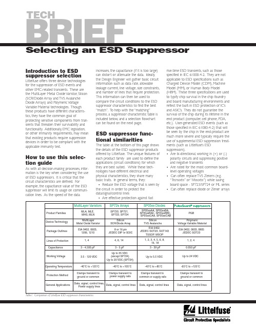
Introduction to ESDsuppressor selectionLittelfuse offers three device technologiesfor the suppression of ESD events andother EMC-related transients.These arethe MultiLayer Metal Oxide Varistor,Silicon(SCR/Diode Array and TVS AvalancheDiode Arrays) and Polymeric VoltageVariable Material technologies.Thoughthese products have different characteris-tics,they have the common goal ofprotecting sensitive components from tran-sients that threaten their survivability andfunctionality.Additionally,EMC legislation,or other immunity requirements,may meanthat existing products require suppressiondevices in order to be compliant with theapplicable immunity test.How to use this selec-tion guideAs with all decision-making processes,infor-mation is the key when considering the useof ESD suppressors.It is critical that thecircuit characteristics are defined.Forexample,the capacitance value of the ESDsuppressor will limit its usage on communi-cation lines.As the speed of the dataincreases,the capacitance (if it is too large)can distort or attenuate the data.Ideally,the Design Engineer will gather basic circuitinformation such as data rate,allowableleakage current,line voltage,size constraints,and number of lines that require protection.This information can then be used tocompare the circuit conditions to the ESDsuppressor characteristics to find the best“match”.T o help with the “matching”process,a suppressor characteristic table isincluded below,and a selection flowchartcan be found on the next page.ESD suppressor func-tional similaritiesThe table at the bottom of this page showsthe details of the ESD suppressor productsoffered by Littelfuse.The unique features ofeach product family are used to define theapplications (circuit conditions) for whichthey are best suited.While these tech-nologies have different electrical andphysical characteristics,they share manybasic traits.In general terms,they:• Reduce the ESD voltage that is seen bythe circuit in order to protect thedata/signal/control lines• Are effective protection against fastrise-time ESD transients,such as thosespecified in IEC 61000-4-2.They are notapplicable to ESD specifications such asCharged Device Model (CDM),MachineModel (MM),or Human Body Model(HBM).These three specifications are usedto typify chip survival in the chip foundryand board manufacturing environments andreflect the built-in ESD protection of IC’sand ASIC’s.They do not guarantee thesurvival of the chip during its lifetime in theend product (computer,cell phone,PDA,etc.).User-generated ESD events (such asthose specified in IEC 61000-4-2) that willbe seen by the chip in the end-product aremuch more severe and typically require theuse of supplemental ESD suppression treat-ments (such as Littelfuse’s ESDsuppressors).• Are bi-directional,working in (+) or (-)polarity circuits and suppressing positiveand negative transients• Are rated for the most common board-level operating voltages• Can often replace TVS Zeners (e.g.“Transorbs”or “Mosorbs”) while savingboard space - SP723/SP724 or ML series• Can often replace diode or Zener arrays Selecting an ESD SuppressorTECHBRIEFSpecifications, descriptions and illustrative material in this literature are as accurate as known at time of publication, but are subject to change without notice. Littelfuse is a registered trademark of Littelfuse Incorporated.EC623A Copyright ©2001 Littelfuse, Inc., All Rights Reserved. Printed in U.S.A. JANUARY2002。
电源保护器数据手册说明书

Electrostatic Discharged Protection Devices (ESD) Data SheetDescriptionUDT26A05L05 is surge rated diode arrays designed to protect high speed data interfaces. It has been specifically designed to protect sensitive components which is connected to data and transmission lines from overvoltage caused by electrostatic discharge (ESD), electrical fast transients (EFT), and lightning.The unique design of the device incorporates one surge rated, and four data lines. Low capacitance steering diodes and a TVS diode in a single package. The low capacitance array configuration allows the user to protect four high speed data or transmission lines.Features● IEC61000-4-2 ESD 15KV Air, 8KV contact compliance ● SOT23-6L surface mount package● Protects four high-speed data lines and one power line ● Array of surge rated, low capacitance diodes ● Working voltage: 5V ● Low leakage current ● Low clamping voltage ● Solid-state silicon avalanche technology ● Lead Free/RoHS compliant● Solder reflow temperature: Pure Tin-Sn, 260~270℃ ● Flammability rating UL 94V-0● Meets MSL level 1, per J-STD-020 ● Marking: B 05B or 054Applications● USB power and data line protection ● 10/100/1000 Ethernet ● Video line protection ● I 2C bus protection● WAN/LAN equipment ● ISDN S/T interface● Microcontroller input protection ● Portable electronicsMaximum RatingsRatingSymbolValue UnitESD voltage (Contact discharge) V ESD ±8kVESD voltage (Air discharge)±15Storage & operating temperature rangeT STG ,T J -55~+150℃Pin ConfigurationElectrical Characteristics (T J=25℃)Parameter Symbol Condition Min. Typ. Max. UnitReverse stand-off voltage V RWM 5V Reverse breakdown voltage V BR I BR=1mA 6 V Reverse leakage current I R V R=5V 5 μAClamping voltage (tp=8/20μs) V C I PP=1A 9.8V Clamping voltage (tp=8/20μs) V C I PP=2A 16VOff state junction capacitance C J 0Vdc,f=1MHzBetween I/Opins and GND2.5 pFApplications InformationESD Protection StandardsIEC61000-4-2Interfaces of consumer electronic equipment are widely specified according to the International Electrotechnical Commission standard IEC61000-4-2. This standard is not targeted towards particular devices but towards general equipment, systems and subsystems that may be involved in electrostatic discharge. consists of a 150pF capacitor and a 330Ω series resistor representing the counterpart to the Device Under Test (DUT).Human Body Model (HBM, MIL-883E method 3015.7)The HBM standard simulates an ESD surge generated by human contact to electronic components.Recommended Soldering ConditionsRecommended ConditionsProfile Feature Pb-Free Assembly Average ramp-up rate (T L to T P) 3℃/second max.Preheat-Temperature Min (T S min) -Temperature Max (T S max) -Time (min to max) (ts)150℃200℃60-180 secondsT S max to T-Ramp-up 3℃/second max.Time maintained above:-Temperature (T-Time (t60-150 seconds Peak Temperature (T P) 260Time within 5 of actual Peak Temperature (t) 20-40 Ramp-down RateTime 25 to Peak TemperatureDimensions (SOT23-6L)Packaging Reel。
君耀电子
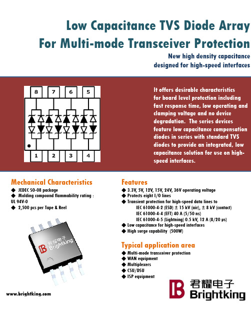
For Multi-mode Transceiver Protection
New high density capacitance designed for high-speed interfaces
Mechanical Characteristics
Typical application area
◆ Multi-mode transceiver protection ◆ WAN equipment ◆ Multiplexers ◆ CSU/DSU ◆ ISP equipment
Application information
© Brightking electronics - January 2008 - Printed in Italy - All rights reserved The Brightking electronics corporate logo is a registered trademark of the Brightking electronics of companies. All other
names are the property of their respective owners. For selected Brightking electronics sales offices :
Brightking (Shenzhen) TEL : +86-755-83795119 . FAX : + 86-755-83791530. shenzhen@; Brightking (Shanghai) TEL : +86-21-63221578. FAX : + 86-21-33040081. shanghai@; Brightking (Beijing) TEL : +8610-62550216#808. FAX : + 86-10-62523764. beijing@; Brightking (Guangzhou) TEL : +86-20-87587379. FAX : + 86-20-87587687. sandy@; Brightking (Taiwan) TEL : +886-2-23911214. FAX : + 886-2-23910964.
DataSheet

NUP4201DR2Low Capacitance Surface Mount TVS for High−Speed Data InterfacesThe NUP4201DR2 transient voltage suppressor is designed to protect equipment attached to high speed communication lines from ESD, EFT, and lightning.Features:•SO−8 Package•Peak Power − 500 Watts 8 x 20 m S•ESD Rating:IEC 61000−4−2 (ESD) 15 kV (air) 8 kV (contact)IEC 61000−4−4 (EFT) 40 A (5/50 ns)IEC 61000−4−5 (lightning) 23 (8/20 m s)•UL Flammability Rating of 94V−0Typical Applications:•High Speed Communication Line Protection•USB Power and Data Line Protection•Video Line Protection•Base Stations•HDSL, IDSL Secondary IC Side Protection •Microcontroller Input ProtectionMAXIMUM RATINGSDevice Package Shipping†ORDERING INFORMATIONNUP4201DR2SO−82500/T ape & Reel†For information on tape and reel specifications, including part orientation and tape sizes, please refer to our Tape and Reel Packaging Specification Brochure, BRD8011/D.ELECTRICAL CHARACTERISTICSELECTRICAL CHARACTERISTICS(T A = 25°C unless otherwise noted)UNIDIRECTIONAL (Circuit tied to Pins 1 and 3 or 2 and 3)TYPICAL CHARACTERISTICS−10009Figure 1. Reverse Breakdown versusTemperature−50T, TEMPERATURE (°C)100200410Figure 2. Reverse Leakage versusTemperatureV Z , R E V E R S E B RE A K D O W N (V )876543210−100−5050100T, TEMPERATURE (°C)200501502385670150I R , R E V E R S E L E A K A G E (m A )Figure 3. 8 × 20 m s Pulse Waveform1009080706050403020100t, TIME (m s)% O F P E A K P U L S E C U R R E N TFigure 4. Clamping Voltage versus Peak PulseCurrent353025201510500204060I PP , PEAK PULSE CURRENT (A)80V C , C L A M P I N G V O L T A G E (V )1030507090APPLICATIONS INFORMATIONThe new NUP4201DR2 device is a low capacitance TVS Diode array designed to protect sensitive electronics such as communications systems, computers, and computer peripherals against damage due to ESD conditions or transient voltage conditions. Because of its low capacitance array configuration, it can be used in high speed I/O data lines.The integrated design of the NUP4201DR2 device offers surge rated, low capacitance steering diodes and a TVS diode integrated in a single package (SO−8). If a transient condition occurs, the steering diodes will drive the transient condition to the positive polarity of the power supply or to ground. The TVS device protects the power line against over−voltage conditions to avoid damage in any downstream components.NUP4201DR2 Device’s Configurations Options The NUP4201DR2 is able to protect up to four data lines against transient over−voltage conditions by driving them to a fixed reference point for clamping purposes. The steering diodes will be forward biased whenever the voltage on the protected line exceeds the reference voltage (Vcc+Vf). The diodes will drive the transient current away from the sensitive circuit.Data lines are connected at pins 1,4,6 and 7. The negative reference is connected at pins 5 and 8. These pins must be connected directly to ground by using a ground plane to minimize the PCB’s ground inductance. It is very important to reduce as much as possible the PCB trace lengths to minimize parasitic inductances.Option 1Four Data lines protection and power supply protection using Vcc as reference.I/O 1I/O 2I/O 3I/O 4V CCFor this configuration, connect pins 2 & 3 directly to the positive supply rail (Vcc), the data lines are referenced to the supply voltage. The internal TVS diode prevents over−voltage on the supply rail.Option 2Four Data lines protection with Bias and power supply isolation resistor.10 KThe NUP4201DR2 device can be isolated from the power supply by connecting a series resistor between pins 2 & 3 and Vcc. A resistor of 10K W is recommended for isolation purposes. The internal TVS and steering diodes remain biased, which provides the advantage of lower capacitance.Option 3Four Data lines protection using internal TVS diode as reference.I/O 1I/O 2I/O 3I/O 4In the case of applications in which a positive supply reference is not available or full isolation is required, the internal TVS could be used as the reference, so for this purpose, the pins 2 and 3 are not connected. In this case, the steering diodes will conduct whenever the voltage on the protected line exceeds the working voltage of the TVS plus one diode drop (Vc=Vf + V TVS ).“Rail to Rail” Protection TopologyThe following figure shows a case when discrete diodesare configured for rail to rail protection on an I/O line:V ESD ESD Upon the above figure, it is possible to observe that if a positive ESD condition occurs, the D1 diode will be forward biased while the D2 diode will be biased when a negative ESD condition occurs. A valid first approximation of the resulting clamping voltage due to the protection diodes can be made as follows:For positive pulse conditions:Vc = Vcc + VfFor negative pulse conditions:Vc = −VfIt is important to mention that effects of parasitic inductances must be considered for fast rise time transient conditions because the clamping voltage on the protected circuit will be different than in the previous case. A valid approximation of the resulting clamping voltage can be made as show below:For positive pulse conditions:Vc = Vcc + Vf + (L di ESD /dt)For negative pulse conditions:Vc = −Vf – (L di ESD /dt)As shown in the formulas, the clamping voltage (Vc) not only depends on the Vf of the steering diodes but also in the L di ESD /dt factor, so this is why it is very important to havea good board layout to minimize the effects of the parasitic inductances.Nevertheless, some disadvantages are still present when discrete diodes are used to suppress ESD conditions in “rail to rail” configuration. If the ESD current is too high, it can potentially result in the damage of any components connected to that rail and it is also possible to experience damage in the discrete diodes if their power dissipation capability is exceeded.The NUP4201DR2 On Semiconductor’s device provides a concept named “RailClamp” which is designed to eliminate the disadvantages of the usage of discrete diodes for ESD protection. The RailClamp concept is achieved with the integration of the TVS device in together with thesteering diodes.Rail to Rail Protection with integrated TBS to achieve the RailClamp conceptDuring an ESD condition, the ESD current will be driven to ground through the TVS device, so the resulting clamping voltage on the protected IC will be:Vc = V F(RailClamp) + V TVS .The clamping voltage of the TVS device is shown as part of the specifications of the NUP4201DR2 datasheet. The clamping voltage will depend on the magnitude of the ESD current. The steering diodes are fast switching devices with unique forward voltage and low capacitance characteristics.TYPICAL APPLICATIONSUPSTREAM USB PORTDOWNSTREAM USB PORTDOWNSTREAM USB PORTESD Protection for USB PortTI/E1 Interface ProtectionPACKAGE DIMENSIONSSO−8CASE 751−07ISSUE ABNOTES:1.DIMENSIONING AND TOLERANCING PER ANSIY14.5M, 1982.2.CONTROLLING DIMENSION: MILLIMETER.3.DIMENSION A AND B DO NOT INCLUDE MOLDPROTRUSION.4.MAXIMUM MOLD PROTRUSION 0.15 (0.006) PERSIDE.5.DIMENSION D DOES NOT INCLUDE DAMBARPROTRUSION. ALLOWABLE DAMBARPROTRUSION SHALL BE 0.127 (0.005) TOTAL INEXCESS OF THE D DIMENSION AT MAXIMUMMATERIAL CONDITION.6.751−01 THRU 751−06 ARE OBSOLETE. NEWSTANDAARD IS 751−07DIMAMIN MAX MIN MAXINCHES4.805.000.1890.197MILLIMETERSB 3.80 4.000.1500.157C 1.35 1.750.0530.069D0.330.510.0130.020G 1.27 BSC0.050 BSCH0.100.250.0040.010J0.190.250.0070.010K0.40 1.270.0160.050M0 8 0 8N0.250.500.0100.020S 5.80 6.200.2280.244 YM0.25 (0.010)Z S X S____*For additional information on our Pb−Free strategy and solderingdetails, please download the ON Semiconductor Soldering andMounting Techniques Reference Manual, SOLDERRM/D.SOLDERING FOOTPRINT*ǒmminchesǓSCALE 6:1ON Semiconductor and are registered trademarks of Semiconductor Components Industries, LLC (SCILLC). SCILLC reserves the right to make changes without further notice to any products herein. SCILLC makes no warranty, representation or guarantee regarding the suitability of its products for any particular purpose, nor does SCILLC assume any liability arising out of the application or use of any product or circuit, and specifically disclaims any and all liability, including without limitation special, consequential or incidental damages.“Typical” parameters which may be provided in SCILLC data sheets and/or specifications can and do vary in different applications and actual performance may vary over time. All operating parameters, including “Typicals” must be validated for each customer application by customer’s technical experts. SCILLC does not convey any license under its patent rights nor the rights of others. SCILLC products are not designed, intended, or authorized for use as components in systems intended for surgical implant into the body, or other applications intended to support or sustain life, or for any other application in which the failure of the SCILLC product could create a situation where personal injury or death may occur. Should Buyer purchase or use SCILLC products for any such unintended or unauthorized application, Buyer shall indemnify and hold SCILLC and its officers, employees, subsidiaries, affiliates, and distributors harmless against all claims, costs, damages, and expenses, and reasonable attorney fees arising out of, directly or indirectly, any claim of personal injury or death associated with such unintended or unauthorized use, even if such claim alleges that SCILLC was negligent regarding the design or manufacture of the part. SCILLC is an Equal Opportunity/Affirmative Action Employer. This literature is subject to all applicable copyright laws and is not for resale in any manner.PUBLICATION ORDERING INFORMATION。
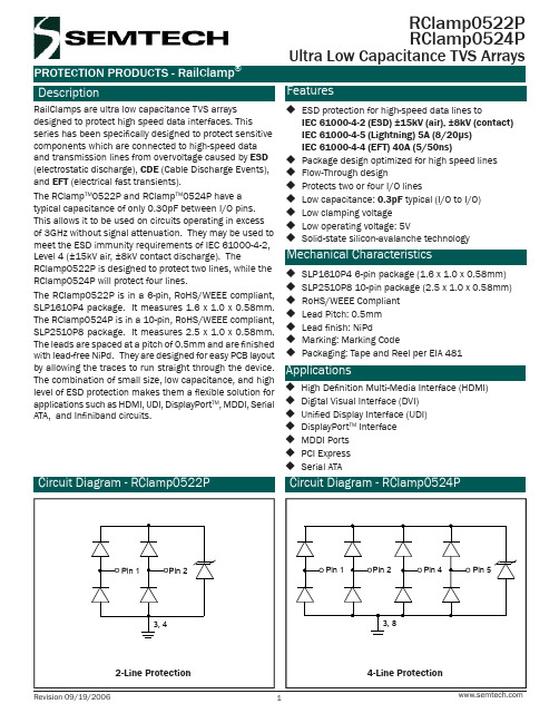
RCLAMP0522P中文资料
Applications
High Definition Multi-Media Interface (HDMI) Digital Visual Interface (DVI) Unified Display Interface (UDI) DisplayPortTM Interface MDDI Ports PCI Express Serial ATA
RClamp0522P RClamp0524P
PRELIMINARY
Power Derating Curve
110 100 90 80 70 60 50 40 30 20 10 0
PROTECTION PRODUCTS Typical Characteristics
Non-Repetitive Peak Pulse Power vs. Pulse Time
Pin 1
Pin 2
Pin 1
Pin 2
Pin 4
Pin 5
3, 4
3, 8
Circuit Diagram
Circuit Diagram
Ordering Information
Part Number RClamp0522P.TCT RClamp0524P.TCT Number of Lines Qty per Reel Reel Size 7 Inch 7 Inch
PRELIMINARY
RClamp0522P RClamp0524P
RClamp0524P
10 9 8 7 6
1
Pin 1-2 5-6 3-4
2
3
Identification Input Lines Output Lines (No Internal Connection) Ground Pin
Semtech 主要保护类芯片
Semtech 主要保护类芯片今天的移动通信集成电路(IC)更高速,更有效率,消耗更少的功率,并且体积比以往更小。
然而,在提高集成电路工艺和芯片的性能存在一个值得注意的问题:增加了静电放电,电缆放电和雷电的危害性。
不仅是晶体管的几何尺寸缩小以惊人的速度发展,导致更敏感的芯片出现,而且更大推广芯片的性需要提高芯片的保护功能。
随着这种趋势的发展,高性能的系统瞬态电压保护将比以往任何时候更加需要。
Semtech 瞬态电压保护芯片,满足了业界最苛刻的要求,该厂家产品是行业中领先的最先进的设备之一,保护电路免受静电放电,电快速瞬变脉冲群,雷电,电缆放电和其他电气过应力等的影响, 能满足行业的最严格的保护标准,包括•IEC 61000-4-2 (ESD)•IEC 61000-4-4 (EFT)•IEC 61000-4-5 (lightning)•Telcordia GR-1089•ITU K.20, K.21主要电气特性:•5V,2.5V,3.3V 等解决方案•超低电容装置;•极低钳位电压•静电放电保护+电磁/射频干扰滤波•单线和多线保护•小封装解决方案,包括Semtech 特有的无引线封装•批量制造•应用固态硅雪崩技术•即指令兼容典型应用:•笔记本•以太网•机顶盒•高清电视/显示器接口:高清晰度多媒体接口/数字化视像接口/显示接口•电信/数据通信接口•服务器/台式电脑常用的元器件如下:主要元件介绍及其应用如下:意法半导体(STM)USB 保护芯片USBLC6意法半导体STM 生产的USBLC6-2SC6,USBLC6-2P6,USBLC6-4SC6 是一个低电容的ESD 保护IC,该产品使用SOT-23/SOT-666 的微型封装,用于保护USB2.0 高速接口的两条数据线路和电源轨。
USBLC6 的典型电容2.5pF,能够确保480-Mbit/s 数据传输速率的USB2.0 信号没有任何失真,这款产品的防静电放电防护电压达到IEC61000-4-2 第4 级15kV 标准。
RCLAMP0524J.TCT中文资料

Cj
Conditions
Any I/O pin to ground
It = 1mA Any I/O pin to ground
VRWM = 5V, T=25°C Any I/O pin to ground
IPP = 1A, tp = 8/20μs Any I/O pin to ground
V = 0V, f = 1MHz R
Dimensions
Circuit Diagram
2.70 0.40
12
1.00
0.60 0.20
0.50
0.58
Pin 1
Pin 2
Pin 3
Pin 4
GND
Nominal Dimensions in mm
Revision 02/05/2008
1
4-Line Protection
3 2: -0.062 dB
1
2
1.8 GHz
3: -0.1087 dB 2.5 GHz
100 MHz
13 GHz GHz
STOP 3000.000000 MHz
RClamp0524J
PRELIMINARY
Insertion Loss S21 - I/O to GND
CH1 S21 LOG 6 dB / REF 0 dB
Mechanical Characteristics
SLP2710P8 8-pin package (2.7 x 1.0 x 0.58mm) RoHS/WEEE Compliant Lead Pitch: 0.5mm Lead finish: NiPdAu Marking: Marking Code Packaging: Tape and Reel per EIA 481
RCLamp0508M.TBT资料

1.8 1.6 1.4 1.2 1 0.8 0.6 0.4 0.2 0 0 1 2 3 4 f = 1 MHz 5
2.00
4.00
6.00
8.00
10.00
12.00
Forward Current - IF (A)
Reverse Voltage - VR (V)
Power Derating Curve
Peak Pulse Power - PPP (kW)
1
0.1
0.01 0.1 1 10 Pulse Duration - tp (µs) 100 1000
0
25
50
75
100
125
150
Ambient Temperature - TA (oC)
Pulse Waveform
30.00 Clamping Voltage -Vc (V) 25.00 20.00 15.00 10.00 5.00 0.00 0.00 Waveform Parameters: tr = 8µs td = 20µs 2.00 4.00 6.00 8.00 10.00 12.00
Percent of I
CH1 S21 LOG 20 dB/ REF 0 dB
START
.030 000 MHz
STOP 3 RT
.030 000 MHz
STOP 3 000. 000 000 MHz
2008 Semtech Corp.
4
RClamp0508M
e-t
Peak Pulse Current - Ipp (A)
Forward Voltage vs. Forward Current
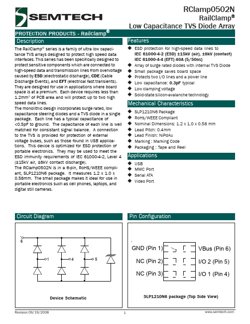
RCLAMP0502N中文资料
1.6
1.4
1.2
1
0.8
0.6
0.4
0.2 f = 1 MHz
0
0
1
2
3
4
5
6
7
Reverse Voltage - VR (V)
CJ(VR) / CJ(VR=0)
CJ(VR) / CJ(VR=0)
Forward Voltage - VF V)
% of Rated Power or IPP
RClamp0502N
40
35
30
25
20
15
Waveform
10
Parameters:
tr = 8μs
5
td = 20μs
0
0
0.5
1
1.5
2
2.5
3
3.5
4
Peak Pulse Current - IPP (A)
Normalize Capacitance vs. Reverse Voltage I/O to Gnd - Pin 4, 5 to Pin 1
Forward Voltage
VF
If = 15mA
Any I/O to pin 6
Clamping Voltage
VC
IPP = 1A, tp = 8/20μs
Any I/O pin to Ground
Clamping Voltage
VC
IPP = 3A, tp = 8/20μs
Any I/O pin to Ground
RClamp0502N
RailClamp® Low Capacitance TVS Diode Array
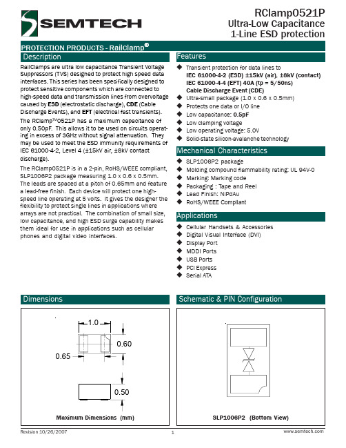
RCLAMP0521P中文资料
Typical 9.3
Maximum 5 11
Units V V
0.025
1
µA
15
V
25
V
0.30
0.50
pF
2007 Semtech Corp.
2
元器件交易网
RClamp0521P
Clamping Voltage - VC (V)
PROTECTION PRODUCTS Typical Characteristics
I/O Line
RClamp0521P
RClamp0521P Spice Model
Parameter IS BV VJ RS IBV CJO TT M N EG
RClamp0521P Spice Parameters
Unit
Rating Peak Pulse Power (tp = 8/20µs) Peak Pulse Current (tp = 8/20µs) ESD per IEC 61000-4-2 (Air) ESD per IEC 61000-4-2 (Contact) Operating Temperature Storage Temperature
ground loops. z The ESD transient return path to ground should be
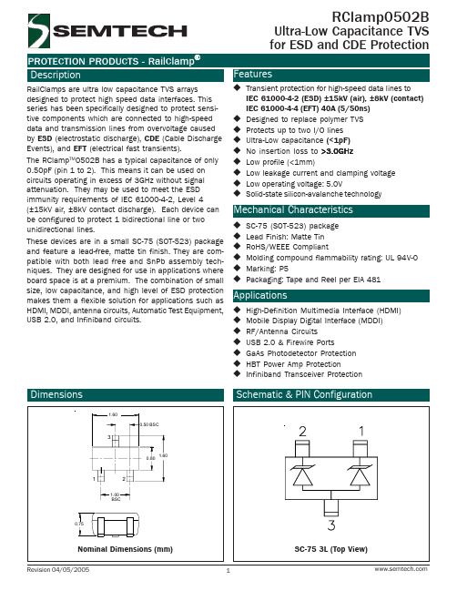
RCLAMP0502B中文资料
Clamping Voltage Clamping Voltage Clamping Voltage Junction Capacitance Junction Capacitance
Symbol V
RWM
VBR
IR
VC VC VC Cj Cj
Conditions
Pin 1 or Pin 2 to Pin 3 and Between Pins 1 and 2
It =1mA Pin 1 or Pin 2 to Pin 3 and Between Pins 1 and 2
VRWM = 5V, T=25°C Pin 1 or Pin 2 to Pin 3 and Between Pins 1 and 2
ESD Response (4kV Contact per IEC 61000-4-2)
RClamp0502B
Insertion Loss S21 (Pin 1 or Pin 2 to Pin 3)
CH1 S21 LOG 6 dB / REF 0 dB
0 dB -6 dB
1: .00460 dB 900 MHz
Applications
High-Definition Multimedia Interface (HDMI) Mobile Display Digital Interface (MDDI) RF/Antenna Circuits USB 2.0 & Firewire Ports GaAs Photodetector Protection HBT Power Amp Protection Infiniband Transceiver Protection
SEMTECH 以太网保护器件资料
Rating Peak Pulse Power (tp = 8/20µs) Peak Pulse Current (tp = 8/20µs) Peak Forward Voltage (IF = 1A, tp=8/20µs) Lead Soldering Temperature Operating Temperature Storage Temperature
tr = 8µs td = 20µs
5 10 15 20 25 30 35 40 45 50 Forward Current - IF (A)
Forward Voltage - V F (V)
Clamping Voltage - VC (V)
% Change in Capacitance
% of Rated Power or IPP
2. The SR05 can be isolated from the power supply by adding a series resistor between pin 4 and VCC. A value of 10kΩ is recommended. The internal TVS and steering diodes remain biased, providing the advantage of lower capacitance.
常用半导体功能术语

肖特基二极管(Schottky Diode)Symbol Parameter 中文VRRM Peak repetitive reverse voltage 反向重复峰值电压VRWM Working peak reverse voltage 方向工作峰值电压VR DC Blocking Voltage 反向直流电压VR(RMS) RMS Reverse Voltage 反向电压有效值IF(AV) Average Rectified Forward Current 正向平均电流IR Reverse Current 反向电流IFSM Non-Repetitive Peak Forward Surge Current 正向浪涌电流VF Forward Voltage 正向直流电压Cj Typical Junction Capactiance 结电容PD Power Dissipation 耗散功率Tj Operating Junction Temperature 工作结温Tstg Storage Temperature Range 存储温度Rth(j-a) Thermal Resistance from Junction to Ambient 结到环境的热阻Pin二极管(Pin Diode)Symbol Parameter 中文VR Continuous reverse voltage 反向直流电压IF Continuous forward current 正向直流电流VF Forward voltage 正向电压IR Reverse current 反向电流Cd diode capacitance 二极管电容rd diode forward resistance 二极管正向电阻Ptot total power dissipation 总的功率损耗Tj Junction Temperature 结温Tstg storage temperature 存储温度TVS二极管(TVS Diode)Symbol Parameter 中文IPP Maximum reverse peak pulse current 峰值脉冲电流VC Clampling voltage 钳位电压IR Maximum reverse leakage current 最大反向漏电流VBR Breakdown voltage 击穿电压VRWM Working peak reverse voltage 反向工作峰值电压VF Forward voltage 正向电压IF Forward current 正向电流IT Test current 测试电流可控硅(SCR)Symbol Parameter 中文VDRM Peak repetitive off-state voltage 断态重复峰值电压VRRM Peak repetitive reverse voltage 反向重复峰值电压IT(RMS) RMS On-state current 额定通态电流ITSM Non repetitive surge peak on-state current 通态非重复浪涌电流IGM Forward peak gate current 控制极重复峰值电流VTM peak forward on-state voltage 通态峰值电压IGT Gate trigger current 控制极触发直流电流VGT Gate trigger voltage 控制极出发电压IH Holding current 维持电流IDRM Peak repetitive off-state current 断态重复峰值电流IRRM Peak repetitive reverse current 反向重复峰值电流PG(AV) Average gate power dissipation 控制极平均功率Tj operating junction temperature range 工作结温Tstg Tstg storage temperature range 存储温度三端稳压管(Three Terminal Voltage Regulator)Symbol Parameter 中文VI input voltage 输入电压Vo output voltage 输出电压△ Load regulation 输出调整率Vo△ Line regulation 输入调整率VoIq quiescent current 偏置电流△ quiescent current change 偏置电流变化量IqVN Output noise voltage 输出噪声电压RR Ripple rejection 纹波抑制比Vd dropout voltage 降落电压Isc short circuit current 短路输出电流Ipk peak current 峰值输出电流Topr operating junction temperature range 结温Tstg storage temperature range 存储温度43系列稳压管(Adjustable Shunt Regulator)Symbol Parameter 中文VKA Cathode voltage 阴极电压IK Cathode current range(continous) 阴极电流Iref Reference input current range,continous 基准输入电流PD Power dissipation 耗散功率Rth(j-a) Thermal resistance from junction to ambient 结到环境的热阻Topr operating junction temperature range 工作结温Tstg storage temperature range 存储温度Vref Reference input voltage 基准输入电压Vref(dev)△Deviation of reference input voltage over full temperature range 全温度范围内基准输入电压的偏差Vref/VKA△△Ratio of change in reference input voltage to the change in cathode voltage 基准输入电压变化量与阴极电压变化量的比Ire△f(dev) Deviation of reference input current over full temperature range 全温度范围内基准输入电流的偏差Imin Minimum cathode current for regulation 稳压时最小负极电流Ioff Off-state cathode current 关断状态阴极电流|ZKA| Dynamic impedance 动态阻抗普通晶体管(Transistor)Symbol Parameter 中文VCBO Collector-Base voltage 发射极开路,集电极-基极电压VCEO Collector-emitter voltage 基极开路,集电极-发射极电压VEBO Emitter-base voltage 集电极开路,发射极-基极电压IC Collector current 集电极电流PC Collector power dissipation 集电极耗散功率Tj Junction temperature 结温Tstg storage temperature 存储温度V(BR)CBO Collector-Base breakdown voltage 发射极开路,集电极-基极反向电压V(BR)CEO Collector-emitter breakdown voltage 基极开路,集电极-发射极反向电压V(BR)EBO Emitter-base breakdown voltage 集电极开路,发射极-基极反向电压ICBO Collector cut-off current 发射极开路,集电极-基极截止电流IEBO Emitter cut-off current 集电极开路,发射极-基极截止电流ICEO Collector cut-off current 基极开路,集电极-发射极截止电流hFE DC current gain 共发射极正向电流传输比的静态值VCEsat Collector-emitter saturation voltage 集电极-发射极饱和电压VBEsat Base-emitter saturation voltage 基极-发射极饱和电压VBE Base-emitter voltage 基极-发射极电压fT Transition frequency 特征频率Cobo Collector output capacitance 共基极输出电容Cibo Collector input capacitance 共基极输入电容F Noise figure 噪声系数ton Turn-on time 开通时间toff Turn-off time 关断时间tr Rise time 上升时间ts Storage time 存储时间tf Fall time 下降时间td Delay time 延迟时间数字晶体管(Digital Transistor)Symbol Parameter 中文VCC Supply voltage 直流电压VIN input voltage 输入电压IO output current 输出电流PD Power dissipation 功率损耗VI(off) Input-off voltage 输入截止电压VI(on) Input-on voltage 输入开启电压VO(on) output voltage 输出电压II input current 输入电流IO(off) output current 输出截止电流GI DC current gain 直流增益R1 Input resistance 输入电阻R2/R1 Resistance ratio 电阻率fT Transition frequency 传输频率Tj junction temperature 结温Tstg storage temperature range 存储温度VCBO Collector-base voltage 发射极开路,集电极-基极反向击穿电压VCEO Collector-emitter voltage 基极开路,集电极-发射极反向击穿电压VEBO Emitter-base voltage 集电极开路,发射极-基极反向击穿电压场效应管(MOSFET)Symbol Parameter 中文ID Continous drain current 漏极直流电流VGS Gate-source voltage 栅-源电压VDS Drain-source voltage 漏-源电压EAS single pulse avalchane energy 单脉冲雪崩击穿能量Rth(j-a) Thermal resistance from junction to ambient 结到环境的热阻Rth(j-c) Thermal resistance from junction to case 结到管壳的热阻V(BR)DSS Drain-source breakdown voltage 漏源击穿电压V(GS)th Gate threshold voltage 栅源阈值电压IGSS Gate-body leakage current 漏-源短路的栅极电流IDSS Zero gate voltage drain curent 栅-源短路的漏极电流rDS(on) Drain-source on-resistance 漏源通态电阻gfs Forward transconductance 跨导VSD Diode forward voltage 漏源间体内反并联二极管正向压降Ciss Input capacitance 栅-源电容Coss Output capacitance 漏-源电容Crss Reverse transfer capacitance 反向传输电容Rg Gate resistance 栅极电阻td(on) Turn-on delay time 开通延迟时间tr Rise time 上升时间td(off) Turn-off delay time 关断延迟时间tf Fall time 下降时间IDM Pulsed drain current 最大脉冲漏电流PD Power dissipation 耗散功率Tj operating junction temperature range 结温Tstg storage temperature range 存储温度。
RCLAMP0504F中文资料
e-t
td = IPP/2
5
10
15
20
25
30
Time (µs)
Forward Voltage vs. peak Pulse Current
8
7
6
5
4
3
Waveform
2
Parameters:
tr = 8µs
1
td = 20µs
0
0
1
2
3
4
5
6
Peak Pulse Current - IPP (A)
25
V
3
pF
1.5
pF
© 2008 Semtech Corp.
2
元器件交易网
PROTECTION PRODUCTS Typical Characteristics
Non-Repetitive Peak Pulse Power vs. Pulse Time
IPP = 6A, tp = 8/20μs Any pin to pin 2
VR = 0V, f = 1MHz Any I/O pin to pin 2
V = 0V, f = 1MHz R
Between I/O pins
Minimum 6
Typical
Maximum 5
Units V V
3
μA
15
V
RClamp0504F
Insertion Loss S21 (I/O to I/O)
CH1 S21 LOG 6 dB / REF 0 dB
START. 030 MHz
STOP 3000.000000 MHz
低电压TVS手册
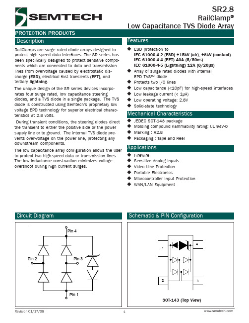
SR2.8RailClampLow Capacitance TVS Diode ArrayRailClamps are surge rated diode arrays designed toprotect high speed data interfaces. The SR series hasbeen specifically designed to protect sensitive compo-nents which are connected to data and transmissionlines from overvoltage caused by electrostatic dis-charge (ESD), electrical fast transients (EFT), andtertiary lightning.The unique design of the SR series devices incorpo-rates four surge rated, low capacitance steeringdiodes, and a TVS diode in a single package. The TVSdiode is constructed using Semtech’s proprietary lowvoltage EPD technology for superior electrical charac-teristics at 2.8 volts.During transient conditions, the steering diodes directthe transient to either the positive side of the powersupply line or to ground. The internal TVS diode pre-vents over-voltage on the power line, protecting anydownstream components.The low capacitance array configuration allows the userto protect two high-speed data or transmission lines.The low inductance construction minimizes voltageovershoot during high current surges.FirewireSensitive Analog InputsVideo Line ProtectionPortable ElectronicsMicrocontroller Input ProtectionWAN/LAN EquipmentESD protection toIEC 61000-4-2 (ESD) ±15kV (air), ±8kV (contact)IEC 61000-4-4 (EFT) 40A (5/50ns)IEC 61000-4-5 (Lightning) 12A (8/20µs)Array of surge rated diodes with internalEPD TVS diodeProtects two I/O linesLow capacitance (<10pF) for high-speed interfacesLow leakage current (< 1µA)Low operating voltage: 2.8VSolid-state technologyJEDEC SOT-143 packageMolding compound flammability rating: UL 94V-0Marking : R2.8Packaging : Tape and ReelAbsolute Maximum RatingElectrical Characteristics8.2RSr e t ema r aP l o bmy S s n o i t i d n oC mum i n iM l a c i p y T mum i x aM s t i nUe g a t l o Vf f O-d n a t Se s r e v eR VMWR8.2Ve g a t l o Vh g u o r h T-h c n u P VT P IT PAµ2=0.3Ve g a t l o Vk c aB-p a n S VBS IBSAm5=8.2Vt n e r r u Ce g a k a e Le s r e v eR IR VMWRC°52=T,V8.2=1Aµe g a t l o Vg n i pma l C VC IP Psµ02/8=p t,A1=0.5Ve g a t l o Vg n i pma l C VC IP Psµ02/8=p t,A5=5.8Ve c n a t i c a p a Cn o i t c n u J Cjd n as n i pO/I n e ew t eBd n u o r GVRz HM1=f,V0=601F ps n i pO/I n e ew t eBVRz HM1=f,V0=3F pg n i t aR l o bmy S e u l a V s t i nU)sµ02/8=p t(r ewo Pe s l u Pk a e P Pk p2s t t aW)sµ02/8=p t(t n e r r u Ce s l u Pk a e P IP P41AI(e g a t l o Vd r aw r o Fk a e PF)sµ02/8=p t,A1=VP F5.1Ve r u t a r e pme Tg n i r e d l o Sd ae L TL).c e s01(62C°e r u t a r e pme Tg n i t a r e pO TJ521+o t55-C°e r u t a r e pme Te g a r o t S TG T S51+o t55-C°Typical CharacteristicsNon-Repetitive Peak Pulse Power vs. Pulse TimePower Derating Curve0.010.11100.11101001000Pulse Duration - t p (µs)P e a k P u l s e P o w e r - P p k (k W)1020304050607080901001100255075100125150Ambient Temperature - T A (oC)% o f R a t e d P o w e r o r I P PClamping Voltage vs. Peak Pulse Current0102030405060708090100110051015202530T im e (µs)P e r c e n t o f I P PPulse WaveformForward Voltage vs. Forward Current0246810121416182005101520Peak Pulse Current - I PP (A)C l a m p i n g V o l t a ge - V C (V )01234567891005101520253035404550Forward Current - I F (A)F o r w a r d V o l t a ge - V F (V )Applications InformationData Line Pr Data Line Pro o t ection Using Int ection Using Internal T ernal T ernal TVV S Diode as ReferenceFigure 1 - EPD TVS IV Characteristic Curve Device Connection Options for Protection of T w o High-Speed Data LinesThe SR2.8 TVS is designed to protect two data lines from transient over-voltages by clamping them to a fixed reference. When the voltage on the protected line exceeds the reference voltage (plus diode V F ) the steering diodes are forward biased, conducting the transient current away from the sensitive circuitry.Data lines are connected at pins 2 and 3. The nega-tive reference (REF1) is connected at pin 1. This pin should be connected directly to a ground plane on the board for best results. The path length is kept as short as possible to minimize parasitic inductance.The positive reference (REF2) is connected at pin 4.The options for connecting the positive reference are as follows:Note that pins 4 is connected internally to the cathode of the low voltage TVS. It is not recommended that this pin be directly connected to a DC source greater than the snap-back votlage (V SB ) as the device can latch on as described below.EPD TVS CharacteristicsThese devices are constructed using Semtech’sproprietary EPD technology. By utilizing the EPD tech-nology, the SR2.8 can effectively operate at 2.8V while maintaining excellent electrical characteristics.The EPD TVS employs a complex nppn structure in contrast to the pn structure normally found in tradi-tional silicon-avalanche TVS diodes. Since the EPD TVS devices use a 4-layer structure, they exhibit aslightly different IV characteristic curve when compared to conventional devices. During normal operation, the device represents a high-impedance to the circuit up to the device working voltage (V RWM ). During an ESDevent, the device will begin to conduct and will enter a low impedance state when the punch through voltage (V PT ) is exceeded. Unlike a conventional device, the low voltage TVS will exhibit a slight negative resistance characteristic as it conducts current. This characteris-tic aids in lowering the clamping voltage of the device,but must be considered in applications where DC voltages are present.When the TVS is conducting current, it will exhibit a slight “snap-back” or negative resistancecharacteristics due to its structure. This point is defined on the curve by the snap-back voltage (V SB )and snap-back current (I SB ). To return to a non-conducting state, the current through the device must fall below the I SB (approximately <50mA) and thevoltage must fall below the V SB (normally 2.8 volts for a 3.3V device). If a 3.3V TVS is connected to 3.3V DC source, it will never fall below the snap-back voltage of 2.8V and will therefore stay in a conducting state.Applications Information (continued)Board Layout Considerations for ESD Protection Board layout plays an important role in the suppression of extremely fast rise-time ESD transients. Recall that the voltage developed across an inductive load is proportional to the time rate of change of current through the load (V = L di/dt). The total clamping voltage seen by the protected load will be the sum of the TVS clamping voltage and the voltage due to theparasitic inductance (VC(TOT) = VC+ L di/dt) . Parasiticinductance in the protection path can result in signifi-cant voltage overshoot, reducing the effectiveness of the suppression circuit. An ESD induced transient for example reaches a peak in approximately 1ns. For a 30A pulse (per IEC 61000-4-2 Level 4), 1nH of series inductance will increase the effective clamping voltage by 30V(V = 1x10⁻⁹ (30/1x10-9)). For maximum effectiveness, the following board layout guidelines are recom-mended:z Minimize the path length between the SR3.3 and the protected line.z Place the SR2.8 near the connector to restrict transient coupling in nearby traces.z Minimize the path length (inductance) between the RJ45 connector and the SR2.8.Matte Tin Lead FinishMatte tin has become the industry standard lead-free replacement for SnPb lead finishes. A matte tin finish is composed of 100% tin solder with large grains. Since the solder volume on the leads is small com-pared to the solder paste volume that is placed on the land pattern of the PCB, the reflow profile will be determined by the requirements of the solder paste. Therefore, these devices are compatible with both lead-free and SnPb assembly techniques. In addition, unlike other lead-free compositions, matte tin does not have any added alloys that can cause degradation of the solder joint.Outline Drawing - SOT-143Contact InformationSemtech Corporation Protection Products Division200 Flynn Road, Camarillo, CA 93012Phone: (805)498-2111 FAX (805)498-3804t r a P r e b m u N h s i n i F d a e L r e p y t Q l e e R e z i S l e e R C T .8.2R S b P n S 000,3h c n I 7TC T .8.2R S ee r F b P 000,3hc n I 7Marking Codesre b m u N t r a P g n i k r a M e d o C 8.2R S 8.2R Ordering Information。
三极管参数符号汇总
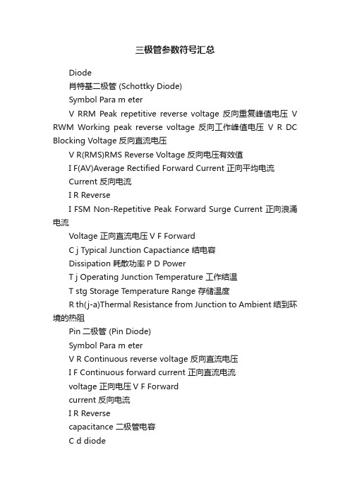
三极管参数符号汇总Diode肖特基二极管 (Schottky Diode)Symbol Para m eterV RRM Peak repetitive reverse voltage 反向重复峰值电压V RWM Working peak reverse voltage 反向工作峰值电压V R DC Blocking Voltage 反向直流电压V R(RMS)RMS Reverse Voltage 反向电压有效值I F(AV)Average Rectified Forward Current 正向平均电流Current 反向电流I R ReverseI FSM Non-Repetitive Peak Forward Surge Current 正向浪涌电流Voltage 正向直流电压V F ForwardC j Typical Junction Capactiance 结电容Dissipation 耗散功率P D PowerT j Operating Junction Temperature 工作结温T stg Storage Temperature Range 存储温度R th(j-a)Thermal Resistance from Junction to Ambient 结到环境的热阻Pin二极管 (Pin Diode)Symbol Para m eterV R Continuous reverse voltage 反向直流电压I F Continuous forward current 正向直流电流voltage 正向电压V F Forwardcurrent 反向电流I R Reversecapacitance 二极管电容C d dioder d diode forward resistance 二极管正向电阻P tot total power dissipation 总的功率损耗T emperature 结温T j Junction temperature 存储温度T stg storageTVS二极管 (TVS Diode)Symbol Para m eterI PP Maximum reverse peak pulse current 峰值脉冲电流voltage 钳位电压V C ClamplingI R Maximum reverse leakage current 最大反向漏电流voltage 击穿电压V(BR) BreakdownV RWM Working peak reverse voltage 反向工作峰值电压V F Forwardvoltage 正向电压current 正向电流I F Forwardcurrent 测试电流I T Test可控硅(SCR)Symbol Para m eterV DRM Peak repetitive off-state voltage 断态重复峰值电压V RRM Peak repetitive reverse voltage 反向重复峰值电压I T(RMS)RMS On-state current 额定通态电流I TSM Non repetitive surge peak on-state current 通态非重复浪涌电流I GM Forward peak gate current 控制极重复峰值电流V TM peak forward on-state voltage 通态峰值电压I GT Gate trigger current 控制极触发直流电流V GT Gate trigger voltage 控制极触发电压current 维持电流I H HoldingI DRM Peak repetitive off-state current 断态重复峰值电流I RRM Peak repetitive reverse current 反向重复峰值电流P G(AV)Average gate power dissipation 控制极平均功率Tj operating junction temperature range 工作结温Tstg storage temperature range 存储温度稳压管(Three Terminal Voltage Regulator)Symbol Para m eterV I inputvoltage 输入电压Vo outputvoltage 输出电压ΔVo Loadregulation 输出调整率ΔVo Lineregulation 输入调整率Iq quiescentcurrent 偏置电流ΔIq quiescent current change 偏置电流变化量V N Output noise voltage 输出噪声电压RR Ripplerejection 纹波抑制比Vd dropoutvoltage 降落电压Isc short circuit current 短路输出电流Ipk peakcurrent 峰值输出电流T opr operating junction temperature range 结温T stg storage temperature range 存储温度43系列稳压管(Adjustable Shunt Regulator)Symbol Para m eterV KA Cathodevoltage 阴极电压I K Cathode current range(continous) 阴极电流I ref Reference input current range,continous 基准输入电流P D Powerdissipation 耗散功率R th(j-a)Thermal resistance from junction to ambient 结到环境的热阻T opr operating junction temperature range 工作结温Tstg storage temperature range 存储温度V ref Reference input voltage 基准输入电压ΔV ref(dev)Deviation of reference input voltage over fulltemperature range全温度范围内基准输入电压的偏差ΔV ref/ΔV KA Ratio of change in reference input voltage to the changein cathode voltage基准输入电压变化量与阴极电压变化量的比ΔI ref(dev)Deviation of reference input current over fulltemperature range全温度范围内基准输入电流的偏差I min Minimum cathode current for regulation 稳压时最小负极电流I off Off-state cathode current 关断状态阴极电流|Z KA| Dynamicimpedance 动态阻抗普通晶体管 (T ransistor)Symbol Para m etervoltage 发射极开路,集电极-基极电压V CBO Collector-Basevoltage 基极开路,集电极-发射极电压V CEO Collector-emitter voltage 集电极开路,发射极-基极电压V EBO Emitter-basecurrent 集电极电流I C CollectorP C Collector power dissipation 集电极耗散功率temperature 结温T j JunctionT stg storagetemperature 存储温度V(BR)CBO Collector-Base breakdown voltage 发射极开路,集电极-基极反向电压breakdownvoltage 基极开路,集电极-发射极反向电压V(BR)CEO Collector-emitterV(BR)EBO Emitter-base breakdown voltage 集电极开路,发射极-基极反向电压I CBO Collector cut-off current 发射极开路,集电极-基极截止电流current 集电极开路,发射极-基极截止电流cut-offI EBO EmitterI CEO Collector cut-off current 基极开路,集电极-发射极截止电流h FE DC current gain 共发射极正向电流传输比的静态值saturation voltage 集电极-发射极饱和电压V CEsat Collector-emittersaturation voltage 基极-发射极饱和电压V BEsat Base-emitter voltage 基极-发射极电压V BE Base-emitterf T Transitionfrequency 特征频率C obo Collector output capacitance 共基极输出电容C ibo Collector input capacitance 共基极输入电容figure 噪声系数F Noisetime 开通时间t on Turn-ontime 关断时间t off Turn-offtime 上升时间t r Risetime 存储时间t s Storagetime 下降时间t f Falltime 延迟时间t d Delay数字晶体管(Digital Transistor) Symbol Para m eter voltage 直流电压V CC Supplyvoltage 输入电压V IN inputcurrent 输出电流I O outputdissipation 功率损耗P D Powervoltage 输入截止电压V I(off) Input-offvoltage 输入开启电压V I(on) Input-onvoltage 输出电压V O(on) outputcurrent 输入电流I I inputcurrent 输出截止电流I O(off) outputG I DC current gain 直流增益R1 Inputresistance 输入电阻ratio 电阻率R2/R1 Resistancefrequency 传输频率f T Transitiontemperature 结温T j junctionT stg storage temperature range 存储温度voltage 发射极开路,集电极-基极反向击穿电压V CBO Collector-baseV CEO Collector-emittervoltage 基极开路,集电极-发射极反向击穿电压voltage 集电极开路,发射极-基极反向击穿电压V EBO Emitter-baseMOS管(MOSFET)Symbol Para m eterI D Continousdraincurrent 漏极直流电流V GS Gate-sourcevoltage 栅-源电压V DS Drain-sourcevoltage 漏-源电压E AS single pulse avalchane energy 单脉冲雪崩击穿能量R th(j-a)Thermal resistance from junction to ambient 结到环境的热阻R th(j-c)Thermal resistance from junction to case 结到管壳的热阻V(BR)DSS Drain-source breakdown voltage 漏源击穿电压V(GS)th Gate threshold voltage 栅源阈值电压I GSS Gate-body leakage current 漏-源短路的栅极电流I DSS Zero gate voltage drain curent 栅-源短路的漏极电流r DS(on) Drain-sourceon-resistance 漏源通态电阻g fs Forwardtransconductance 跨导V SD Diode forward voltage 漏源间体内反并联二极管正向压降C iss Inputcapacitance 栅-源电容C oss Outputcapacitance 漏-源电容C rss Reverse transfer capacitance 反向传输电容R g Gate resistance 栅极电阻t d(on)Turn-on delay time 开通延迟时间t r Risetime 上升时间t d(off)Turn-off delay time 关断延迟时间t f Falltime 下降时间I DM Pulsed drain current 最大脉冲漏电流P D Power dissipation 耗散功率T j operating junction temperature range 结温T stg storage temperature range 存储温度。
- 1、下载文档前请自行甄别文档内容的完整性,平台不提供额外的编辑、内容补充、找答案等附加服务。
- 2、"仅部分预览"的文档,不可在线预览部分如存在完整性等问题,可反馈申请退款(可完整预览的文档不适用该条件!)。
- 3、如文档侵犯您的权益,请联系客服反馈,我们会尽快为您处理(人工客服工作时间:9:00-18:30)。
SR05RailClampLow Capacitance TVS Diode ArrayRailClamps are surge rated diode arrays designed toprotect high speed data interfaces. The SR series hasbeen specifically designed to protect sensitive compo-nents which are connected to data and transmissionlines from overvoltage caused by ESD (electrostaticdischarge), EFT (electrical fast transients), and light-ning.The unique design of the SR series devices incorpo-rates four surge rated, low capacitance steering diodesand a TVS diode in a single package. During transientconditions, the steering diodes direct the transient toeither the positive side of the power supply line or toground. The internal TVS diode prevents over-voltageon the power line, protecting any downstream compo-nents.The low capacitance array configuration allows the userto protect two high-speed data or transmission lines.The low inductance construction minimizes voltageovershoot during high current surges.!USB Power & Data Line Protection!Ethernet 10BaseT!I2C Bus Protection!Video Line Protection!T1/E1 secondary IC Side Protection!Portable Electronics!Microcontroller Input Protection!WAN/LAN Equipment!ISDN S/T Interface!ESD protection to IEC 61000-4-2, Level 4!Array of surge rated diodes with internal TVS Diode!Protects two I/O lines!Low capacitance (<10pF) for high-speed interfaces!Low clamping voltage!Low operating voltage: 5.0V!Solid-state silicon-avalanche technology!JEDEC SOT-143 package!UL 497B listed!Molding compound flammability rating: UL 94V-0!Marking : R05!Packaging : Tape and Reel per EIA 481Absolute Maximum RatingElectrical Characteristics5RSr e t ema r aP l o bmy S s n o i t i d n oC mum i n iM l a c i p y T mum i x aM s t i nUe g a t l o Vf f O-d n a t Se s r e v eR VMWR5Ve g a t l o Vnwo d k a e r Be s r e v eR VRB ItAm1=6Vt n e r r u Ce g a k a e Le s r e v eR IR VMWRC°52=T,V5=5Aµe g a t l o Vg n i pma l C VC IP Psµ02/8=p t,A1=8.9Ve g a t l o Vg n i pma l C VC IP Psµ02/8=p t,A01=21Ve g a t l o Vg n i pma l C VC IP Psµ02/8=p t,A52=02Ve c n a t i c a p a Cn o i t c n u J Cjd n as n i pO/I n e ew t eBd nGVRz HM1=f,V0=601F ps n i pO/I n e ew t eBVRz HM1=f,V0=3F pg n i t aR l o bmy S e u l a V s t i nU)sµ02/8=p t(r ewo Pe s l u Pk a e P Pk p5s t t aW)sµ02/8=p t(t n e r r u Ce s l u Pk a e P IP P52AI(e g a t l o Vd r aw r o Fk a e PF)sµ02/8=p t,A1=VP F5.1Ve r u t a r e pme Tg n i r e d l o Sd ae L TL).c e s01(62C°e r u t a r e pme Tg n i t a r e pO TJ521+o t55-C°e r u t a r e pme Te g a r o t S TG T S51+o t55-C°Typical CharacteristicsNon-Repetitive Peak Pulse Power vs. Pulse TimePower Derating Curve0.010.11100.11101001000Pulse Duration - tp (µs)P e a k P u l s e P o w e r - P P P (k W)01020304050607080901001100255075100125150Ambient Temperature - T A (oC)% o f R a t e d P o w e r o r I P PClamping Voltage vs. Peak Pulse Current0102030405060708090100110051015202530Time (µs)P e r c e n t o f I P PPulse Waveform01234567891005101520253035404550Forward Current - I F (A)F o r w a r d V o l t a ge - V F (V )Forward Voltage vs. Forward CurrentCapacitance vs. Reverse Voltage01234567891005101520253035404550Forward Current - I F (A)F o r w a r d V o l t ag e - V F (V )-16-14-12-10-8-6-4-200123456Reverse Voltage (V)% C h a n g e i nC a p a c i t a n c eDevice Connection Options for Protection of Two High-Speed Data LinesThe SR05 TVS is designed to protect two data lines from transient over-voltages by clamping them to a fixed reference. When the voltage on the protected line exceeds the reference voltage (plus diode V F ) the steering diodes are forward biased, conducting the transient current away from the sensitive circuitry.Data lines are connected at pins 2 and 3. The nega-tive reference (REF1) is connected at pin 1. This pin should be connected directly to a ground plane on the board for best results. The path length is kept as short as possible to minimize parasitic inductance.The positive reference (REF2) is connected at pin 4.The options for connecting the positive reference are as follows:1.To protect data lines and the power line, connectpin 4 directly to the positive supply rail (V CC ). In this configuration the data lines are referenced to the supply voltage. The internal TVS diode prevents over-voltage on the supply rail.2.The SR05 can be isolated from the power supply byadding a series resistor between pin 4 and V CC . A value of 10k Ω is recommended. The internal TVS and steering diodes remain biased, providing the advantage of lower capacitance.3.In applications where no positive supply referenceis available, or complete supply isolation is desired,the internal TVS may be used as the reference. In this case, pin 4 is not connected. The steering diodes will begin to conduct when the voltage on the protected line exceeds the working voltage of the TVS (plus one diode drop).ESD Protection With RailClampsRailClamps are optimized for ESD protection using the rail-to-rail topology. Along with good board layout,these devices virtually eliminate the disadvantages of using discrete components to implement this topology.Consider the situation shown in Figure 1 where dis-crete diodes or diode arrays are configured for rail-to-rail protection on a high speed line. During positive duration ESD events, the top diode will be forward biased when the voltage on the protected line exceeds the reference voltage plus the V F drop of the diode.Data Line and Power Supply Protection Using Vcc as referenceData Line Protection with Bias and Power Supply Isolation ResistorData Line Protection Using Internal TVS Diode as ReferenceApplications InformationFor negative events, the bottom diode will be biased when the voltage exceeds the V F of the diode. At first approximation, the clamping voltage due to the charac-teristics of the protection diodes is given by:V C= V CC + V F (for positive duration pulses)V C = -V F(for negative duration pulses)However, for fast rise time transient events, theeffects of parasitic inductance must also be consid-ered as shown in Figure 2. Therefore, the actual clamping voltage seen by the protected circuit will be:V C = V CC + V F + L P di ESD /dt (for positive duration pulses)V C = -V F - L G di ESD /dt (for negative duration pulses)ESD current reaches a peak amplitude of 30A in 1ns for a level 4 ESD contact discharge per IEC 1000-4-2.Therefore, the voltage overshoot due to 1nH of series inductance is:V = L P di ESD /dt = 1X10⁻⁹ (30 / 1X10⁻⁹) = 30VExample:Consider a V CC = 5V, a typical V F of 30V (at 30A) for the steering diode and a series trace inductance of 10nH.The clamping voltage seen by the protected IC for a positive 8kV (30A) ESD pulse will be:V C = 5V + 30V + (10nH X 30V/nH) = 335VThis does not take into account that the ESD current is directed into the supply rail, potentially damaging any components that are attached to that rail. Also note that it is not uncommon for the V F of discrete diodes to exceed the damage threshold of the protected IC. This is due to the relatively small junction area of typical discrete components. It is also possible that the power dissipation capability of the discrete diode will be exceeded, thus destroying the device.The RailClamp is designed to overcome the inherent disadvantages of using discrete signal diodes for ESD suppression. The RailClamp’s integrated TVS diode helps to mitigate the effects of parasitic inductance inFigure 1 - “Rail-Figure 1 - “Rail-T T o-Rail” Pr o-Rail” Pro o t ection T ection Topologyopology (First Approximation)Figure 2 - The Effects of Parasitic Inductance When Using Discrete Components to ImplementRail-Rail-T T o-Rail Pr o-Rail Pro o t ection Figure 3 - Rail-Figure 3 - Rail-T T o-Rail Pr o-Rail Proo t ection Using RailClam RailClamp T p T V S Arra S Arraysys Applications Information (continued)Applications Information (continued)the power supply connection. During an ESD event,the current will be directed through the integrated TVS diode to ground. The total clamping voltage seen by the protected IC due to this path will be:V C = V F(RailClamp) + V TVSThis is given in the data sheet as the rated clamping voltage of the device. For a SR05 the typical clamping voltage is <16V at I PP =30A. The diodes internal to the RailClamp are low capacitance, fast switching devices that are rated to handle transient currents and main-tain excellent forward voltage characteristics.Universal Serial Bus ESD ProtectionThe figure below illustrates how to use the SR05 to protect one upstream USB port and the SRDA05-4 to protect two downstream USB ports. When the voltage on the data lines exceed the bus voltage (plus one diode drop), the internal rectifiers are forward biased conducting the transient current away from the pro-tected controller chip. The TVS diode directs the surge to ground. The TVS diode also acts to suppress ESD strikes directly on the voltage bus. Thus, both power and data pins are protected with a single device.Reference Semtech application note SI96-18 for further information.Typical ApplicationsOutline Drawing - SOT-143Contact InformationSemtech Corporation Protection Products Division652 Mitchell Rd., Newbury Park, CA 91320Phone: (805)498-2111 FAX (805)498-3804t r a P r e b m u N g n i k r o W e g a t l o V r e p y t Q l e e R e z i S l e e R C T .50R S V 5000,3h c n I 7GT .50R S V5000,01hc n I 31Marking Codesre b m u N t r a P g n i k r a M e d o C 50R S 50R Ordering InformationThis datasheet has been downloaded from: Datasheets for electronic components.。
