x part 3 Swap
c语言swap用法 -回复

c语言swap用法-回复C语言中的swap用法Swap(交换)是在编程中常用的一个概念,它用于交换两个变量的值,以实现数据的调换或排序等操作。
在C语言中,swap的用法并不复杂,但理解其原理对于提高程序的效率和正确性却是非常重要的。
在本文中,我将一步一步回答关于C语言中swap的用法。
1. 交换两个变量的值最常见的用法是交换两个变量的值。
假设我们有两个变量a和b,我们想要交换它们的值。
下面是一个基本的swap函数的定义:cvoid swap(int *a, int *b) {int temp;temp = *a;*a = *b;*b = temp;}在这个函数中,我们使用了一个临时变量temp。
首先,temp的值被设置为变量a的值。
然后,通过指针的方式,将变量a的值设置为变量b的值。
最后,将变量b的值设置为temp的值,从而实现了a和b的值的交换。
在实际调用swap函数的时候,我们需要将变量的地址作为参数传递给函数。
cint main() {int a = 1;int b = 2;printf("Before swap: a = d, b = d\n", a, b);swap(&a, &b);printf("After swap: a = d, b = d\n", a, b);return 0;}输出结果为:Before swap: a = 1, b = 2After swap: a = 2, b = 1通过swap函数,我们实现了变量a和b的值的交换,从而得到了我们想要的结果。
2. 交换数组的元素除了交换两个变量的值,swap函数也可以用于交换数组中的元素。
在这种情况下,我们需要将数组的地址作为参数传递给swap函数,并指定要交换的元素的索引。
下面是一个例子:cvoid swap(int *arr, int i, int j) {int temp;temp = arr[i];arr[i] = arr[j];arr[j] = temp;}在这个函数中,我们通过一个临时变量temp,交换了数组中索引为i和j 的两个元素的值。
swapper2分区及利用
巧建虚拟内存,提高手机运行速度。
作者:木棉藤吉时间:2011-7-25 11:18:00 编辑:木棉藤吉来源:网络转载DroidSwap是用来解决仅配备256MB RAM及以下的安卓手机,运行太多应用程序造成后台软件自动关闭、运行不流畅及卡等现象,尤其适合HTC G1(192MB RAM)、G2和G3(288MB RAM)、华为U8500(256MB RAM)等运行内存较小的安卓手机其他也可使用。
1.合理设置swap分区:DroidSwap的使用方法与“一键省电”类似,都是只需按一下按钮即可看到效果,不过在使用前需要简单设置:安装好该APK软件后,按“Menu”键进入“Configuration”(配置),在下拉菜单中选择“Swap place”选项,为新分区起个好记的名字即可。
2.设置虚拟内存大小:接着进入“Swap size”选项设置分区大小,此处建议将分区大小设置在64MB以下。
注意,笔者测试过选择96MB或128MB,均出现适得其反的效果,虚拟内存太大,读取速度变慢,性能会下降。
但如果是高速卡可选256MB,普通卡建议最大128MB,比较稳定。
3.一键启动Swap分区:在主界面单击顶部“ON”按钮开始启动Swap分区。
整个过程大约持续1-2分钟,期间会有几个“Fail”(失败);不要惊慌,这是因为DroidSwap 需先加载后取得ROOT权限所致。
第一次“ON”显示完成后,再一次单击“ON”直到出现“ALL DONE”启动成功。
用过Linux系统的机油都知道,Linux系统为了最大程度的适用低配置机器,而专门设置了了一个Swap交换分区,以减少对硬件的要求。
Android是基于Linux的,这种方式同样可以应用在Android手机里。
也就是扩展Android手机硬件的内存空间!Swap分区是什么?Swap分区,即交换区,Swap空间的作用可简单描述为:当系统的物理内存不够用的时候,就需要将物理内存中的一部分空间释放出来,以供当前运行的程序使用。
swap分区操作流程
swap分区操作流程Swap分区操作流程1. 什么是Swap分区?Swap分区是一种在操作系统中使用的虚拟内存技术,它可以将部分系统内存空间作为硬盘上的一部分空间使用,用作内存扩展。
当系统内存不足时,Swap分区可以将部分不常用的数据移出内存,从而释放出更多内存供其他应用程序使用。
2. 创建Swap分区要创建Swap分区,需要按照以下步骤进行操作:•打开终端或命令行界面•输入以下命令以创建一个新的Swap分区文件:sudo fallocate -l [大小] [文件路径],例如:sudo fallocate -l 2G/swapfile•输入以下命令使Swap分区只能被管理员读写:sudo chmod 600 /swapfile•输入以下命令以将文件转换为Swap分区:sudo mkswap /swapfile•输入以下命令以启用Swap分区:sudo swapon /swapfile3. 查看Swap分区信息要查看Swap分区的信息,可以执行以下步骤:•打开终端或命令行界面•输入以下命令以查看Swap分区信息:sudo swapon --show 4. 调整Swap分区如果需要调整Swap分区的大小或禁用Swap分区,可以按照以下步骤进行操作:调整Swap分区大小•打开终端或命令行界面•输入以下命令以禁用当前的Swap分区:sudo swapoff /swapfile•输入以下命令以调整Swap分区文件的大小:sudo fallocate -l [新大小] /swapfile•输入以下命令以将文件转换为Swap分区:sudo mkswap /swapfile•输入以下命令以重新启用Swap分区:sudo swapon /swapfile 禁用Swap分区•打开终端或命令行界面•输入以下命令以禁用Swap分区:sudo swapoff /swapfile•输入以下命令以删除Swap分区文件:sudo rm /swapfile5. 总结Swap分区是一种重要的虚拟内存技术,它可以有效扩展系统内存空间。
SWAP设置

Swapper 是设置高速缓存区的工具。
Linux中的Swap(即:交换分区),类似于Windows 的虚拟内存,就是当内存不足的时候,把一部分硬盘空间虚拟成内存使用,从而解决内存容量不足的情况。
Android是基于Linux的操作系统,所以也可以使用Swap分区来提升系统运行效率。
如果一个程序长时间没有活动,就会被置换到Swap分区(或Swap文件), 释放出内存以提高当前程序的性能“扩展内存”用于非应用程序(例如播放器+浏览器+地图等),需要高级权限及SD卡。
注意:使用Swapper 会缩短SD卡寿命。
新版本增加支持开启Swap分区。
功能相当于电脑的虚拟内存。
相对于蹂躏1k+的机子,我更倾向于蹂躏几十块钱的SD卡。
打个比方,用P2P软件下X片对电脑硬盘伤害很大这个大家都知道,但是你会因为这个停止去下片吗?使用方法:有两种设置高速缓存分区的方式:第一种是创建一个Swap文件到SD卡的Fat32分区,大小可以自定义设置。
第一种貌似很多童鞋都不会设置,简单讲下具体设置情况。
有电脑的话我上下图。
进入软件主菜单,点击设置,把swap位置和swap大小设置好。
高级选项→使用swap分区的勾去掉(很多童鞋反应都是fail很大一部分都是这个勾没去掉,,特别注意一下)→返回进入主菜单→创建swap→swap on →获取信息查看是否已经开启成功。
另一种是你的SD卡已经有Swap分区,但是未开启,那么可以使用它来开启1.首先你必须已经有Swap分区,新手可以使用内置分区功能的Recovery分区2.运行Swapper,点击【设置】找到【高级选项】,3.勾选『使用SW AP分区』,点击下面的『SWAP分区』查看是否与你的SD卡分区相对应,在第三分区。
确定后,返回主界面。
4.点击【Swap ON】,最后点击【获取信息】看看是否开启成功。
成功后第四行Swap: 93864KB 本人实测,后台开照相、音乐、网页、QQ等10来个程序,按小房子瞬间返回桌面!不再出现黑屏20秒或者桌面程序长期无响应!运行速度依然流程!每次开机或设置过swap都会关闭,重新点下swap on就可以swap分区不宜过大,因为sd卡的读取速度实在太慢,设置太大的话,会有太多数据滞留在卡内,拖慢慢系统速度。
【洛谷日报#119】浅析Treap
【洛⾕⽇报#119】浅析Treap Treap,⼀种数据结构,⽀持插⼊节点、删除节点、求第x⼤的节点、求权值为x的节点的排名、求权值⽐x⼩的最⼤节点、求权值⽐x⼤的最⼩节点提⽰:以下图⽚均由Powerpoint出品,请原谅丑陋⽆⽐的图【引⼦:⼆叉排序树和堆】⾸先,我们要知道,Treap=Tree+Heap,Tree指的是⼆叉排序树,Heap则是指堆1.Tree——⼆叉排序树⼆叉排序树,是指根的左⼉⼦⽐根⼩,右⼉⼦⽐根⼤,且左右⼦树均为⼆叉排序树的树通俗来说,就是左⼦树全部⽐根⼩,右⼦树全部⽐根⼤,如图:⼆叉排序树这时候,我们要插⼊⼀个节点,就不断地判断与根的⼤⼩关系(假设没有节点相同):1.⽐根⼩,去左⼦树2.⽐根⼤,去右⼦树直到来到⼀个空树,插⼊:插⼊操作删除节点:如果⼀个节点是叶⼦节点,直接销毁否则,如果这个节点有⼀个⼦节点,直接将其连接到该节点的⽗亲否则,沿着右⼦树的根⼀路向左到底,然后⽤那个值替换掉要删除的节点,例如我们要删7:选定8作为7的代替者因为这个点必定⼩于右⼦树的其他值,且⼤于左⼦树的全部数,所以他是作为根的最好⼈选接下来,交换8和7,然后销毁7:交换8和7并删掉7查询x的排名:这个很简单,查看x与根的⼤⼩关系,如果相等,排名为左⼦树元素个数+1⽐根⼩,递归查询他在左⼦树的排名,排名为他在左⼦树的排名,空树排名为0⽐根⼤,递归查询他在右⼦树的排名,排名为右⼦树的排名+左⼦树元素个数+1查询排名为x的数:这个也很好理解,判断左⼦树元素个数是否⼤于等于之如果是就在左⼦树找否则,如果刚好为左⼦树元素个数+1,就是根如果⼤于左⼦树元素个数+1,则必定在右⼦树,这个和查询x排名对照起来就很好理解查询x的前驱(求权值⽐x⼩的最⼤节点):空节点返回-inf如果根的权值⼩于等于x,就在左⼦树找否则,取根和右⼦树查询结果的最⼤值(我们要求最⼤节点)查询x的后继(求权值⽐x⼤的最⼩节点):空节点返回inf如果根的权值⼤于等于x,就去右⼦树否则,取根和左⼦树查询结果的最⼩值(我们要求最⼩节点)我才不会告诉你这两段我是Ctrl C+V的其实上⾯的前驱后继对照看就很好记这时候细⼼的⼈会发现,这六个操作不就是刚刚上⾯讲的Treap⽀持的操作吗?好吧,那如果是这样我们还写个Treap⼲什么?原因看下图退化成为⼀条链**退化成⼀条链了! **恐怕是药丸了,虽然⼀般情况下⼆叉排序树复杂度不错,是但是,不排除有丧⼼病狂的出题⼈故意卡你的情况,这时候复杂度为要怎么办呢?堆!你值得拥有2.Heap——堆堆,⼀种完全⼆叉树(看看看,刚好防⽌了退化),保证根节点⽐左右⼦树都要⼤或⼩,⼤的称为⼤根堆,反之称⼩根堆。
swap大小设置原则

swap大小设置原则在计算机领域中,swap是一个缓存空间,被用作存储一些暂时没有被使用的内存内容。
在某些情况下,计算机内存不足或者请求过多内存时,swap空间就会被应用。
为了更好地使用swap空间,我们需要设置一些原则。
1.根据需要动态设置swap大小swap分区的大小应该根据实际的需要动态设置。
如果内存使用量没有超过物理RAM的80%,则不需要计算机使用swapping。
但是,如果远程访问、虚拟环境或其他应用使计算机需要更多的内存,那么应该动态地增加swap的大小。
在这种情况下,swap空间应该在物理RAM的2倍之下。
如果存在更高的内存压力,可以适当增加swap空间。
但是,也应该注意,如果swap空间过大,将消耗过多的磁盘空间,因此需要在空间和性能之间取得良好的平衡。
2.合理设置交换空间与物理内存为了让swap正常工作,交换空间设置应该考虑到系统的内存容量。
一般的设置规则是将swap设置为物理内存大小的两倍,最大不超过8GB。
在一些老的计算机系统中,物理内存非常小,而swap 空间应该设置在最大物理内存的两倍以内。
3.将swap空间设置在独立的分区上另一种swap大小调整的原则是将swap分区放置在独立的分区上。
这是一个很好的做法,因为如果系统坏了,可以单独恢复swap分区。
此外,可以使用磁盘工具来监测交换空间使用情况,了解系统补丁是否导致了异常。
4.向swap分区中写入数据在某些情况,为提高系统的整体性能,可以将swap设置为独立的SSD或以RAM为基础的文件系统。
无论何种方式,都需要在swap空间中写入数据,以便在任何时候都可以利用这些数据。
如果系统遇到紧急情况,它需要不时地读取交换空间中保存的数据。
当系统在Swap中找到一个以前使用的幸存者(如游戏),它需要将该幸存者从磁盘中读取到物理RAM 中。
5.异常信号或缺少交换空间问题在一些情况下,如果交换空间不足,将报告异常。
管理员应该根据异常信息和系统日志,调整swap分区大小,以避免再次出现这种情况。
利率互换新交易机制——X—Swap系统功能介绍
I RS t r a di n g me c h a ni s m n a me d X— Sw a p s y s t em .Si n c e i t s l a u n ch i n F eb r u a r y 201 4,X— Swa p s y s t em h a s b e e n wi d el y
口 —
O O
0 l
m
- ■I _
l ∞
∞
■_ 嘲
‘ l d , : 1 2
l 4i l : 1 ,
F R o o t3 M
F R o o 6
—
吴 玮
潘墨益
为满足国 内日益增长的利率互换交易需求 ,提高合约标准化和市场透明度 ,全 国银行间同业拆借中心组织业务和开发
团 队经过两年攻关 ,自主研发 了利率互换新交易机制 ( 简称X — S W a p 系统 )。该系统 自2 0 1 4 年2 月运行以来 ,以其友 好的用户界面 、便捷的授信设置 、支持多种订单策略等功能特色提升交易效率和用户体验 ,受到市场一致好评 。
a ppr ai s e d b y mar k e t u s e r s ,gi v i n g c r e di t t o i t s f r i en d l y UI ,e a s y c r e di t s e t an d mu l t i — o r de r s up po r t f ea t u r e s whi c h h a v e gr e a t l y e nh a n c e d t r a di n g e fi ci e n c y an d u s er e x pe r i en c e .
swap的用法

swap的用法
(最新版)
目录
1.swap 的定义与功能
2.swap 的基本用法
3.swap 的扩展用法
4.swap 的注意事项
正文
【1.swap 的定义与功能】
swap 是一个在计算机编程中广泛使用的函数,它的主要作用是交换两个变量的值。
swap 函数在不同的编程语言中可能有不同的名称和语法,但其功能都是类似的。
【2.swap 的基本用法】
swap 的基本用法非常简单,一般形式如下:
`swap(变量 1, 变量 2)`
在执行 swap 函数后,原本的变量 1 的值会变成变量 2 的值,而变量 2 的值会变成变量 1 的值。
【3.swap 的扩展用法】
除了基本的交换值功能外,swap 函数还有一些扩展用法,例如:
- 交换数组元素:通过提供一个数组和两个数组下标,swap 可以交换数组中对应下标的元素值。
- 交换结构体成员:通过提供一个结构体和两个结构体成员名称,swap 可以交换结构体中对应成员的值。
【4.swap 的注意事项】
在使用 swap 函数时,需要注意以下几点:
- 确保要交换的变量或元素是可变的,否则交换操作将无法生效。
- 确保要交换的变量或元素类型相同,否则可能导致程序错误。
swap原理

swap原理
swap(交换)原理是指在某个系统或者环境下,将两个或多
个元素的位置进行互换的操作过程。
这种操作可以应用于不同的场景和数据结构中,例如数组、链表、栈、队列等。
在计算机编程中,swap原理常常用于排序算法中,其中最经
典的就是冒泡排序和快速排序。
冒泡排序中,通过不断交换相邻元素的位置,将较大(或较小)的元素逐渐移到序列的末尾(或起始位置),从而实现排序的目的。
而快速排序则是通过选定一个基准元素,将其他元素分为两个子序列,比基准元素小的移动到左侧,比基准元素大的移动到右侧,然后分别对两个子序列进行递归排序。
在操作系统中,swap原理也被广泛应用于虚拟内存管理中。
为了解决物理内存不足的问题,操作系统会将一部分不常用的数据从内存写入到硬盘的交换空间(Swap Space)中,以释放
出物理内存供其他进程使用。
当需要访问被交换出去的数据时,操作系统会将其重新读取到内存中,而将另一部分不常用的数据进行写回到交换空间中,以实现数据的交换和管理。
总之,swap原理是一种常见的操作,通过交换元素的位置来
实现不同场景下的需求。
它能够应用于排序算法、内存管理、数据结构等多个领域,为系统和程序的性能优化提供了一种有效的手段。
浅析swap内存交换
浅析swap内存交换swap 原理swap 就是内存交换的意思。
计算机对内存分为物理内存与虚拟内存。
物理内存就是计算机的实际内存⼤⼩,虚拟内存则是从磁盘空间开辟出⼀部分内存空间虚拟出来的,所以也叫磁盘缓存。
虚拟内存的出现,让机器内存不够的情况得到部分解决。
程序运⾏的时候系统会在虚拟内存与物理内存直接进⾏替换和加载。
这⾥的虚拟内存就是 swap。
进程运⾏的时候系统会判断当前物理内存是否还有空闲,如果有那么则直接调⼊内存进⾏运⾏;如果没有,那么会根据优先级选择⼀个进程挂起,把该进程交换到 swap 中等待,然后把新的进程调⼊到内存中运⾏。
进程向系统请求内存发现不⾜时,系统会把内存中暂时不⽤的数据交换出去,放在 swap 分区⾥,这个过程称为 swap out(so)当进程⼜需要这些数据且系统发现还有空闲物理内存时,⼜会把 SWAP 分区中的数据交换到物理内存中,这个过程称为 swap in(si)swap 使⽤完,操作系统会触发OOM-Killer机制,杀掉占⽤内存最⼤的进程。
所以⼤家经常会发现内存飙⾼之后进程莫名其妙的不见了。
jvm 与 swap 的关系1:系统内存⾜够 (jvm 内存未使⽤到 swap 内存),但 jvm 内存不够,最终导致 jvm 的频繁垃圾回收(FGC),由于 fullgc 时间很久,会导致线程的长期暂停2:系统内存不够,JVM 堆内存部分⽤到了 swap,此时的垃圾回收需要把 swap 的内存交换到系统物理内存再进⾏ jvm 的垃圾回收。
导致每次 GC 的时间都变得很久3:物理内存不够⽤,⼤量 JVM 的堆内存被交换到 swap 之后,垃圾回收时把 swap 内存交换到物理内存,但 swap 的内存⼜不会⽴即交换回来。
此时 swap 使⽤的内存占⽤会变⼤,可能会导致 oom killer。
IPC-7351B & PCBL Land Pattern Naming Convention

I P C-7351B N a m i n g C o n v e n t i o n f o r S t a n d a r d S M T L a n d P a t t e r n sSurface Mount Land PatternsComponent, Category Land Pattern Name Ball Grid Array’s...............................BGA + Pin Qty + C or N + Pitch P + Ball Columns X Ball Rows _ Body Length X Body Width X Height BGA w/Dual Pitch.BGA + Pin Qty + C or N + Col Pitch X Row Pitch P + Ball Columns X Ball Rows _ Body Length X Body Width X Height BGA w/Staggered Pins..................BGAS + Pin Qty + C or N + Pitch P + Ball Columns X Ball Rows _ Body Length X Body Width X Height BGA Note: The C or N = Collapsing or Non-collapsing BallsCapacitors, Chip, Array, Concave..........................................................CAPCAV + Pitch P + Body Length X Body Width X Height - Pin Qty Capacitors, Chip, Array, Flat..................................................................CAPCAF + Pitch P + Body Length X Body Width X Height - Pin Qty Capacitors, Chip, Non-polarized.................................................................................................CAPC + Body Length + Body Width X Height Capacitors, Chip, Polarized.....................................................................................................CAPCP + Body Length + Body Width X Height Capacitors, Chip, Wire Rectangle........................................................................................CAPCWR + Body Length + Body Width X Height Capacitors, Molded, Non-polarized...........................................................................................CAPM + Body Length + Body Width X Height Capacitors, Molded, Polarized.................................................................................................CAPMP + Body Length + Body Width X Height Capacitors, Aluminum Electrolytic ............................................................................................................CAPAE + Base Body Size X Height Ceramic Flat Packages.....................................................................................................CFP127P + Lead Span Nominal X Height - Pin Qty Column Grid Array’s.....................................................CGA + Pitch P + Number of Pin Columns X Number of Pin Rows X Height - Pin Qty Crystals (2 leads)........................................................................................................................XTAL + Body Length X Body Width X Height Dual Flat No-lead..........................................................................................................DFN + Body Length X Body Width X Height – Pin Qty Diodes, Chip................................................................................................................................DIOC + Body Length + Body Width X Height Diodes, Molded...........................................................................................................................DIOM + Body Length + Body Width X Height Diodes, MELF................................................................................................................................DIOMELF + Body Length + Body Diameter Fuses, Molded............................................................................................................................FUSM + Body Length + Body Width X Height Inductors, Chip.............................................................................................................................INDC + Body Length + Body Width X Height Inductors, Molded........................................................................................................................INDM + Body Length + Body Width X Height Inductors, Precision Wire Wound................................................................................................INDP + Body Length + Body Width X Height Inductors, Chip, Array, Concave..............................................................INDCAV + Pitch P + Body Length X Body Width X Height - Pin Qty Inductors, Chip, Array, Flat......................................................................INDCAF + Pitch P + Body Length X Body Width X Height - Pin Qty Land Grid Array, Round Lead............................LGA + Pin Qty - Pitch P + Pin Columns X Pin Rows _ Body Length X Body Width X Height Land Grid Array, Square Lead........................LGAS + Pin Qty - Pitch P + Pin Columns X Pin Rows _ Body Length X Body Width X Height LED’s, Molded............................................................................................................................LEDM + Body Length + Body Width X Height Oscillators, Side Concave........................................................................OSCSC + Pitch P + Body Length X Body Width X Height - Pin Qty Oscillators, J-Lead.......................................................................................OSCJ + Pitch P + Body Length X Body Width X Height - Pin Qty Oscillators, L-Bend Lead.............................................................................OSCL + Pitch P + Body Length X Body Width X Height - Pin Qty Oscillators, Corner Concave....................................................................................................OSCCC + Body Length X Body Width X Height Plastic Leaded Chip Carriers..................................................PLCC + Pitch P + Lead Span L1 X Lead Span L2 Nominal X Height - Pin Qty Plastic Leaded Chip Carrier Sockets Square.......................PLCCS + Pitch P + Lead Span L1 X Lead Span L2 Nominal X Height - Pin Qty Quad Flat Packages..................................................................QFP + Pitch P + Lead Span L1 X Lead Span L2 Nominal X Height - Pin Qty Ceramic Quad Flat Packages.................................................CQFP + Pitch P + Lead Span L1 X Lead Span L2 Nominal X Height - Pin Qty Quad Flat No-lead................................................................QFN + Pitch P + Body Width X Body Length X Height - Pin Qty + Thermal Pad Pull-back Quad Flat No-lead..............................................PQFN + Pitch P + Body Width X Body Length X Height - Pin Qty + Thermal Pad Quad Leadless Ceramic Chip Carriers..........................................................LCC + Pitch P + Body Width X Body Length X Height - Pin Qty Quad Leadless Ceramic Chip Carriers (Pin 1 on Side)...............................LCCS + Pitch P + Body Width X Body Length X Height - Pin Qty Resistors, Chip...........................................................................................................................RESC + Body Length + Body Width X Height Resistors, Molded......................................................................................................................RESM + Body Length + Body Width X Height Resistors, MELF...........................................................................................................................RESMELF + Body Length + Body Diameter Resistors, Chip, Array, Concave............................................................RESCAV + Pitch P + Body Length X Body Width X Height - Pin Qty Resistors, Chip, Array, Convex, E-Version (Even Pin Size)...............RESCAXE + Pitch P + Body Length X Body Width X Height - Pin Qty Resistors, Chip, Array, Convex, S-Version (Side Pins Diff)................RESCAXS + Pitch P + Body Length X Body Width X Height - Pin Qty Resistors, Chip, Array, Flat.....................................................................RESCAF + Pitch P + Body Length X Body Width X Height - Pin Qty Small Outline Diodes, Flat Lead...................................................................................SODFL + Lead Span Nominal + Body Width X Height Small Outline IC, J-Leaded........................................................................................SOJ + Pitch P +Lead Span Nominal X Height - Pin Qty Small Outline Integrated Circuit, (50 mil Pitch SOIC)......................................................SOIC127P +Lead Span Nominal X Height - Pin Qty Small Outline Packages............................................................................................SOP + Pitch P +Lead Span Nominal X Height - Pin Qty Small Outline No-lead...........................................................SON + Pitch P + Body Width X Body Length X Height - Pin Qty + Thermal Pad Pull-back Small Outline No-lead.........................................PSON + Pitch P + Body Width X Body Length X Height - Pin Qty + Thermal Pad Small Outline Transistors, Flat Lead....................................................................SOTFL + Pitch P + Lead Span Nominal X Height - Pin Qty SOD (Example: SOD3717X135 = JEDEC SOD123)........................................................SOD + Lead Span Nominal + Body Width X Height SOT89 (JEDEC Standard Package).......................................................................................................................................................SOT89 SOT143 & SOT343 (JEDEC Standard Package)..............................................................................................................SOT143 & SOT343 SOT143 & SOT343 Reverse (JEDEC Standard Package)...........................................................................................SOT143R & SOT343R SOT23 & SOT223 Packages (Example: SOT230P700X180-4)...............................SOT + Pitch P + Lead Span Nominal X Height - Pin Qty TO (Generic DPAK - Example: TO228P970X238-3).................................................................TO + Pitch P + Lead Span X Height - Pin QtyI P C-7351B L a n d P a t t e r n N a m i n g C o n v e n t i o n N o t e s•All dimensions are in Metric Units•All Lead Span and Height numbers go two places past the decimal point and “include” trailing Zeros•All Lead Span and Body Sizes go two place before the decimal point and “remove” leading Zeros•All Chip Component Body Sizes are one place to each side of the decimal point•Pitch Values are two places to the right & left of decimal point with no leading Zeros but include trailing zeros N a m i n g C o n v e n t i o n S p e c i a l C h a r a c t e r U s e f o r L a n d P a t t e r n sThe _ (underscore) is the separator between pin Qty in Hidden & Deleted pin componentsThe – (dash) is used to separate the pin qty.The X (capital letter X) is used instead of the word “by” to separate two numbers such as height X width like “Quad Packages”.P C B L i b r a r i e s S u f f i x N a m i n g C o n v e n t i o n f o r L a n d P a t t e r n sCommon SMT Land Pattern to Describe Environment Use (This is the last character in every name)Note: This excludes the BGA component family as they only come in the Nominal Environment Condition •M.................Most Material Condition (Level A)•N..................Nominal Material Condition (Level B)•L.................Least Material Condition (Level C)Alternate Components that do not follow the JEDEC, EIA or IEC Standard•A..................Alternate Component (used primarily for SOP & QFP when Component Tolerance or Height is different) •B..................Second Alternate ComponentReverse Pin Order•-20RN..........20 pin part, Reverse Pin Order, Nominal EnvironmentHidden Pins•-20_24N......20 pin part in a 24 pin package. The pins are numbered 1 – 24 the hidden pins are skipped. The schematic symbol displays up to 24 pins.Deleted Pins•-24_20N......20 pin part in a 24 pin package. The pins are numbered 1 – 20. The schematic symbol displays 20 pins. JEDEC and EIA Standard parts that have several alternate packages•AA, AB, AC.JEDEC or EIA Component IdentifierGENERAL SUFFIXES_HS.........................HS = Land Pattern with Heat Sink attachment requiring additional holes or padsExample: TO254P1055X160_HS-6N_BEC......................BEC = Base, Emitter and Collector (Pin assignments used for three pin Transistors)Example: SOT95P280X160_BEC-3N_SGD......................SGD = Source, Gate and Drain (Pin assignments used for three pin Transistors)Example: SOT95P280X160_SGD-3N_213........................213 = Alternate pin assignments used for three pin TransistorsExample: SOT95P280X160_213-3NP C B L i b r a r i e s N a m i n g C o n v e n t i o n f o r N o n-S t a n d a r d S M T L a n d P a t t e r n s Surface Mount Land PatternsComponent, Category Land Pattern Name Amplifiers....................................................................................................................................................AMP_ Mfr.’s Part Number Batteries......................................................................................................................................................BAT_ Mfr.’s Part Number Capacitors, Variable..................................................................................................................................CAPV_Mfr.’s Part Number Capacitors, Chip, Array, Concave (Pins on 2 or 4 sides)..............................................................CAPCAV_Mfr Series No. - Pin Qty Capacitors, Chip, Array, Flat (Pins on 2 sides)..............................................................................CAPCAF_Mfr Series No. - Pin Qty Capacitors, Miscellaneous............................................................................................................................CAP_Mfr.’s Part Number Crystals......................................................................................................................................................XTAL_Mfr.’s Part Number Diodes, Miscellaneous...................................................................................................................................DIO_Mfr.’s Part Number Diodes, Bridge Rectifiers............................................................................................................................DIOB_Mfr.’s Part Number Ferrite Beads..................................................................................................................................................FB_Mfr.’s Part Number Fiducials......................................................................................................................................FID + Pad Size X Solder Mask Size Filters..............................................................................................................................................................FIL_Mfr.’s Part Number Fuses..........................................................................................................................................................FUSE_Mfr.’s Part Number Fuse, Resettable.....................................................................................................................................FUSER_Mfr.’s Part Number Inductors, Miscellaneous...............................................................................................................................IND_Mfr.’s Part Number Inductors, Chip, Array, Concave (Pins on 2 or 4 sides)..................................................................INDCAV_Mfr Series No. - Pin Qty Inductors, Chip, Array, Flat (Pins on 2 sides).................................................................................INDCAF_Mfr Series No. - Pin Qty Keypad.................................................................................................................................................KEYPAD_Mfr.’s Part Number LEDS............................................................................................................................................................LED_Mfr.’s Part Number LEDS, Chip...................................................................................................................................................LED_Mfr.’s Part Number Liquid Crystal Display...................................................................................................................................LCD_Mfr.’s Part Number Microphones..................................................................................................................................................MIC_Mfr.’s Part Number Opto Isolators............................................................................................................................................OPTO_Mfr.’s Part Number Oscillators......................................................................................................................................OSC_Mfr.’s Part Number - Pin Qty Quad Flat Packages w/Bumper Corners, Pin 1 Side.............BQFP + Pitch P + Lead Span L1 X Lead Span L2 Nominal X Height - Pin Qty Quad Flat Packages w/Bumper Corners, 1 Center..............BQFPC + Pitch P + Lead Span L1 X Lead Span L2 Nominal X Height - Pin Qty Resistors, Chip, Array, Concave (Pins on 2 or 4 sides).................................................................RESCAV_Mfr Series No. - Pin Qty Resistors, Chip, Array, Convex Type E (Pins on 2 sides)...........................................................RESCAXE_Mfr Series No. - Pin Qty Resistors, Chip, Array, Convex Type S (Pins on 2 sides)...........................................................RESCAXS_Mfr Series No. - Pin Qty Resistors, Chip, Array, Flat (Pins on 2 sides)................................................................................RESCAF_Mfr Series No. - Pin Qty Relays.....................................................................................................................................................RELAY_Mfr.’s Part Number Speakers....................................................................................................................................................SPKR_Mfr’s Part Number Switches........................................................................................................................................................SW_Mfr.’s Part Number Test Points, Round......................TP + Pad Size (1 place left of decimal and 2 places right of decimal, Example TP100 = 1.00mm) Test Points, Square...............................................................TPS + Pad Size (1 place left of decimal and 2 places right of decimal) Test Points, Rectangle....................................TP + Pad Length X Pad Width (1 place left of decimal and 2 places right of decimal) Thermistors.............................................................................................................................................THERM_Mfr.’s Part Number Transceivers.............................................................................................................................................XCVR_ Mfr.’s Part Number Transducers (IRDA’s)................................................................................................................................XDCR_Mfr.’s Part Number Transient Voltage S_Mfr.’s Part Number Transient Voltage Suppressors, SP_Mfr.’s Part Number Transistor Outlines, Custom....................................................................................................................TRANS_Mfr.’s Part Number Transformers.............................................................................................................................................XFMR_Mfr.’s Part Number Trimmers & Potentiometers........................................................................................................................TRIM_Mfr.’s Part Number Tuners.....................................................................................................................................................TUNER_Mfr.’s Part Number Varistors.......................................................................................................................................................VAR_Mfr.’s Part Number Voltage Controlled Oscillators.....................................................................................................................VCO_Mfr.’s Part Number Voltage Regulators, Custom......................................................................................................................VREG_Mfr.’s Part NumberI P C-7251N a m i n g C o n v e n t i o n f o r T h r o u g h-H o l e L a n d P a t t e r n sThe land pattern naming convention uses component dimensions to derive the land pattern name.The first 3 – 6 characters in the land pattern name describe the component family.The first number in the land pattern name refers to the Lead Spacing or hole to hole location to insert the component lead.All numbers that follow the Lead Spacing are component dimensions.These characters are used as component body identifiers that precede the value and this is the priority order of the component body identifiers –P = Pitch for components with more than two leadsW = Maximum Lead Width (or Component Lead Diameter)L = Body Length for horizontal mountingD = Body Diameter for round component bodyT = Body Thickness for rectangular component bodyH = Height for vertically mounted componentsQ = Pin Quantity for components with more than two leadsR = Number of Rows for connectorsA, B & C = the fabrication complexity level as defined in the IPC-2221 and IPC-2222Notes:All component body values are in millimeters and go two places to the right of the decimal point and no leading zeros.All Complexity Levels used in the examples are “B”.Component, Category Land Pattern Name Capacitors, Non Polarized Axial Diameter Horizontal Mounting.........CAPAD + Lead Spacing + W Lead Width + L Body Length + D Body Diameter Example: CAPAD800W52L600D150BCapacitors, Non Polarized Axial Diameter; Lead Spacing 8.00; Lead Width 0.52; Body Length 6.00; Body Diameter 1.50Capacitors, Non Polarized Axial Rectangular.........CAPAR + Lead Spacing + W Lead Width + L Body Length + T Body thickness + H Body Height Example: CAPAR800W52L600T50H70BCapacitors, Non Polarized Axial; Lead Spacing 8.00; Lead Width 0.52; Body Length 6.00; Body Thickness 0.50; Body Height 0.70Capacitors, Non Polarized Axial Diameter Vertical Mounting .........CAPADV + Lead Spacing + W Lead Width + L Body Length + D Body Diameter Example: CAPADV300W52L600D150BCapacitors, Non Polarized Axial; Lead Spacing 3.00; Lead Width 0.52; Body Length 6.00; Body Diameter 1.50mmCapacitors, Non Polarized Axial Rect. Vert. Mtg.CAPARV + Lead Spacing + W Lead Width + L Body Length + T Body Thickness + H Body Height Example: CAPARV300W52L600T50H70BCapacitors, Non Polarized Axial Rect. Vertical; Lead Spacing 8.00; Lead Width 0.52; Body Length 6.00; Body Thickness 0.50; Body Height 0.70 Capacitors, Non Polarized Radial Diameter.......................................CAPRD + Lead Spacing + W Lead Width + D Body Diameter + H Body Height Example: CAPRD200W52D300H550BCapacitors, Non Polarized Radial Diameter; lead spacing 2.00; lead width 0.52; Body Diameter 3.00; Height 5.50Capacitors, Non Polarized Radial Rectangular.......CAPRR + Lead Spacing + W Lead Width + L Body Length + T Body thickness + H Body Height Example: CAPRR200W52L50T70H550BCapacitors, Non Polarized Radial Rectangular; lead spacing 2.00; lead width 0.52; Body Length 0.50; Body thickness 0.70; Height 5.50 Capacitors, Non Polarized Radial Disk Button........CAPRB + Lead Spacing + W Lead Width + L Body Length + T Body thickness + H Body Height Example: CAPRB200W52L50T70H550BCapacitors, Non Polarized Radial Rectangular; lead spacing 2.00; lead width 0.52; Body Length 0.50; Body thickness 0.70; Height 5.50 Capacitors, Polarized Axial Diameter Horizontal Mounting................CAPPA + Lead Spacing + W Lead Width + L Body Length + D Body Diameter Example: CAPPAD800W52L600D150BCapacitors, Polarized Axial Diameter; Lead Spacing 8.00; Lead Width 0.52; Body Length 6.00; Body Diameter 1.50Capacitor, Polarized Radial Diameter.................................................CAPPR + Lead Spacing + W Lead Width + D Body Diameter + H Body Height Example: CAPPRD200W52D300H550BCapacitors, Polarized Radial Diameter; lead spacing 2.00; lead width 0.52; Body Diameter 3.00; Height 5.50Diodes, Axial Diameter Horizontal Mounting.......................................DIOAD + Lead Spacing + W Lead Width + L Body Length + D Body Diameter Example: DIOAD800W52L600D150BCapacitors, Non Polarized Axial Diameter; Lead Spacing 8.00; Lead Width 0.52; Body Length 6.00; Body Diameter 1.50Diodes, Axial Diameter Vertical Mounting .........................................DIOADV + Lead Spacing + W Lead Width + L Body Length + D Body Diameter Example: DIOADV300W52L600D150BCapacitors, Non Polarized Axial; Lead Spacing 8.00; Lead Width 0.52; Body Length 6.00; Body Diameter 1.50Dual-In-Line Packages...................................DIP + Lead Span + W Lead Width + P Pin Pitch + L Body Length + H Component Height + Q Pin Qty Example: DIP762W52P254L1905H508Q14BDual-In-Line Package: Lead Span 7.62; Lead Width 0.52; Pin Pitch 2.54; Body Length 19.05; Body Height 5.08; Pin Qty 14Component, Category Land Pattern Name Dual-In-Line Sockets....................................DIPS + Lead Span + W Lead Width + P Pin Pitch + L Body Length + H Component Height + Q Pin Qty Example: DIPS762W52P254L1905H508Q14BDual-In-Line Package Socket: Lead Span 7.62; Lead Width 0.52; Pin Pitch 2.54; Body Length 19.05; Body Height 5.08; Pin Qty 14Headers, Vertical....... HDRV + Lead Span + W Lead Width + P Pin Pitch + R Pins per Row + L Body Length + T Body Thickness + H Component HeightExample: HDRV200W52P200R2L4400T400H900BHeader, Vertical: Lead Span 2.00; Lead Width 0.52; Pin Pitch 2.00; 2 Rows; Body Length 44.00; Body Thickness 4.00; Body Height 9.00 Headers, Right Angle...............HDRRA + Lead Span + W Lead Width + P Pin Pitch + R Pins per Row + L Body Length + T Body Thickness + H Component HeightExample: HDRRA200W52P200R2L4400T400H900BHeader, Vertical: Lead Span 2.00; Lead Width 0.52; Pin Pitch 2.00; 2 Rows; Body Length 44.00; Body Thickness 4.00; Body Height 9.00 Inductors, Axial Diameter Horizontal Mounting....................................INDAD + Lead Spacing + W Lead Width + L Body Length + D Body Diameter Example: INDAD800W52L600D150BInductors, Axial Diameter; Lead Spacing 8.00; Lead Width 0.52; Body Length 6.00; Body Diameter 1.50Inductors, Axial Diameter Vertical Mounting .....................................INDADV + Lead Spacing + W Lead Width + L Body Length + D Body Diameter Example: INDADV300W52L600D150BInductors, Axial Diameter Vertical Mounting; Lead Spacing 3.00; Lead Width 0.52; Body Length 6.00; Body Diameter 1.50Jumpers, Wire...................................................................................................................................................JUMP + Lead Spacing + W Lead Width Example: JUMP500W52BJumper; Lead Spacing 5.00; Lead Width 0.52Mounting Holes Plated With Support Pad..........................................................................MTGP + Pad Size + H Hole Size + Z Inner Layer Pad Size Example: MTGP700H400Z520This is a Mounting hole for a #6-32 screw using a circular 7.00 land on the primary and secondary side of the board, a 4.00 diameter hole with the internal lands are smaller that the external and are also circular 5.20 in diameter.Mounting Holes Non-Plated With Support Pad................................................................MTGNP + Pad Size + H Hole Size + Z Inner Layer Pad Size Example: MTGNP700H400Z520This is a Mounting hole for a #6-32 screw using a circular 7.00 land on the primary and secondary side of the board, a 4.00 diameter hole with the internal lands are smaller that the external and are also circular 5.20 in diameter.Mounting Holes Non-Plated Without Support Pad.....................MTGNP + Pad Size + H Hole Size + Z Inner Layer Pad Size + K Keep-out Diameter Example: MTGNP100H400Z520K700This is a Mounting hole for a #6-32 screw using a circular 1mm land on the primary and secondary side of the board, a 4.00 diameter hole with the internal lands are smaller that the external and are also circular 5.20 in diameter and a 7.00 diameter keep-out.Mounting Holes Plated with 8 Vias .....................................................................MTGP + Pad Size + H Hole Size + Z Inner Layer Pad Size + 8 Vias Example: MTGP700H400Z520V8This is a Mounting hole for a #6-32 screw using a circular 7mm land on the primary and secondary side of the board, a 4mm diameter hole with the internal lands are smaller that the external and are also circular 5.2mm in diameter, with 8 vias.Pin Grid Array’s.............................PGA + Pin Qty + P Pitch + C Pin Columns + R Pin Rows + L Body Length X Body Width + H Component Height Example: PGA84P254C10R10L2500X2500H300BPin Grid Array: Pin Qty 84; Pin Pitch 2.54; Columns 10; Rows 10; Body Length 25.00 X 25.00; Component Height 3.00Resistors, Axial Diameter Horizontal Mounting...................................RESAD + Lead Spacing + W Lead Width + L Body Length + D Body Diameter Example: RESAD800W52L600D150BResistors, Axial Diameter; Lead Spacing 8.00; Lead Width 0.52; Body Length 6.00; Body Diameter 1.50Resistors, Axial Diameter Vertical Mounting ....................................RESADV + Lead Spacing + W Lead Width + L Body Length + D Body Diameter Example: RESADV300W52L600D150BResistors, Axial Diameter Vertical Mounting; Lead Spacing 3.00; Lead Width 0.52; Body Length 6.00; Body Diameter 1.50Resistors, Axial Rectangular Horizontal Mounting...RESAR + Lead Spacing + W Lead Width + L Body Length + T Body thickness + H Body Height Example: RESAR800W52L600T50H70BResistors, Axial Rectangular; Lead Spacing 8.00; Lead Width 0.52; Body Length 6.00; Body Thickness 0.50; Body Height 0.70Test Points, Round Land......................................................................................................................................................................TP + Lead Width Example: TP52Test Points, Square Land..................................................................................................................................................................TPS + Lead Width Example: TPS52Test Points, Top Land Round & Bottom Land Square.....................................................................................................................TPRS + Lead Width Example: TPRS52 Wire....................................................................................................................................................................................................PAD + Wire Width Example: PAD52。
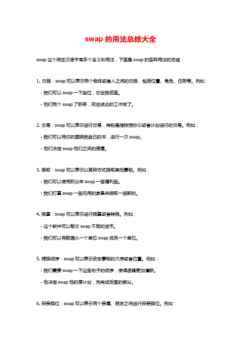
Linuxswap的创建与配置
Linuxswap的创建与配置在Linux下,swap的作⽤类似Windows系统下的“虚拟内存”。
当物理内存不⾜时,拿出部分硬盘空间当SWAP分区(虚拟成内存)使⽤,从⽽解决内存容量不⾜的情况。
Linux下的swap有两种实现形式,⼀种是通过某个物理磁盘分区来实现swap,另⼀种是通过虚拟内存⽂件来实现swap。
⼀、物理磁盘分区来实现swap1、通过分区软件创建⼀个分区,分区类型fdisk下为82,gdisk下为8200,partep分区标记没有定义swap,其实分区后不更改分区类型也⾏测试也可以⽤,但为了在分区⼯具下⽅便查看最好还是把分区类型改成swap对应的分区类型,本⼈理解分区类型就是分区软件下⽤来描述分区所要承载的⽂件系统的类型,⽐如分区类型为83表⽰为linxu分区,⽤于格式化成ext3 ext4等linux⽂件系统,分区创建的⽅法这⾥就不写了前⾯有分区创建的⽅法。
2、使⽤mkswap命令把分区格式化为swap分区-------------------------------------------------------------------root@debian:~# mkswap /dev/sdb1Setting up swapspace version 1, size = 1024 MiB (1073737728 bytes) #交换分区的容量为1Gno label, UUID=47fe2c83-c4b9-4ee5-ad91-4a9642f66df5root@debian:~#-------------------------------------------------------------------3、使⽤swapon命令使交换分区/dev/sdb1⽣效-------------------------------------------------------------------root@debian:~# free -h #查看没加前swap容量 total used free shared buff/cache availableMem: 2.0G 250M 1.4G 8.5M 311M 1.6GSwap: 2.0G 0B 2.0G #没加前容量为2Groot@debian:~# swapon /dev/sdb1 #使新添加的swap⽣效root@debian:~# free -h #查看添加完后的容量 total used free shared buff/cache availableMem: 2.0G 250M 1.4G 8.5M 311M 1.6GSwap: 3.0G 0B 3.0G #添加完容量变成了3Groot@debian:~#-------------------------------------------------------------------4、Linux swapon命令参数及⽤法swapon 是开启swap,相对的便有⼀个关闭swap的指令,swapoffswapon [选项] [设备]-h 显⽰帮助信息-V 显⽰版本信息-v 显⽰详细模式-s 显⽰swap的使⽤情况,可以查看所有激活的swap-a 将/etc/fstab⽂件中所有设置为swap的设备启⽤-p 设定优先权,你可以在0到32767中间选⼀个数字给他。
c语言swap用法 -回复

c语言swap用法-回复C语言Swap用法在C语言中,swap(交换)是一种常见的操作,它允许我们交换两个变量的值。
这种操作非常有用,可以在许多编程场景下发挥作用。
它可以用于排序算法,优化算法等。
在本文中,我们将一步一步地回答关于C语言swap用法的问题,以便更好地理解它。
一、什么是Swap操作?Swap操作是指交换两个变量的值。
例如,如果有两个变量a和b,我们可以使用swap操作将它们的值互换。
通过此操作,变量a将拥有变量b 的值,而变量b将拥有变量a的值。
这种操作是通过临时变量来完成的。
具体而言,我们将两个变量的值存储在临时变量中,然后将它们互相赋值,从而实现交换。
二、为什么要使用Swap操作?交换操作非常有用,它可以在许多编程问题中发挥作用。
在排序算法中,我们经常需要交换两个元素的位置以实现排序。
此外,在优化算法中,也使用交换操作来改变变量的值以找到更好的解决方案。
总之,交换操作是一种通用的技术,可以在许多编程场景中帮助我们解决问题。
三、如何使用Swap操作?在C语言中,我们可以使用指针或传值的方式实现Swap操作。
1. 使用指针方式进行Swap操作:使用指针方式进行Swap操作有助于我们直接修改变量的值,而不需要创建临时变量。
下面是使用指针方式进行Swap操作的示例代码:c#include <stdio.h>void swap(int *a, int *b){int temp = *a;*a = *b;*b = temp;}int main(){int x = 5, y = 10;printf("Before swap: x = d, y = d\n", x, y);swap(&x, &y);printf("After swap: x = d, y = d\n", x, y);return 0;}在这个例子中,我们定义了一个swap函数,它接收两个指针作为参数。
swap的用法总结大全
swap的用法总结大全swap这个词在汉语中有多个含义和用法,下面是swap的各种用法的总结:1. 交换:swap可以表示两个物体或者人之间的交换,包括位置、角色、任务等。
例如: - 我们可以swap一下座位,你坐我后面。
- 他们两个swap了职务,现在彼此的工作变了。
2. 交易:swap可以表示进行交易,特别是指按照协议或者计划进行的交易。
例如:- 我们可以用你的画换我自己的书,进行一次swap。
- 他们决定swap他们之间的房屋。
3. 换取:swap可以表示以某种方式换取其他事物。
例如:- 我们可以使用积分来swap一些福利品。
- 我们打算swap一些无用的家具来换取一些新的。
4. 换算:swap可以表示进行换算或者转换。
例如:- 这个软件可以帮你swap不同的货币。
- 我们可以将数据从一个单位swap成另一个单位。
5. 掉换顺序:swap可以表示改变事物的次序或者位置。
例如:- 我们需要swap一下这些句子的顺序,使得逻辑更加清晰。
- 他决定swap他的原计划,先完成后面的部分。
6. 探亲换位:swap可以表示两个亲属、朋友之间进行探亲换位。
例如:- 我和我的朋友计划明年进行一次swap,我去她的城市,她来我的城市。
7. 讨债:swap可以表示还钱或者补偿。
例如:- 我们需要尽快swap借款,以免产生更多的利息。
- 我们要把这个坏掉的东西swap还给对方。
8. 切换:swap可以表示切换到其他的状态或者模式。
例如:- 你可以通过按下这个按钮来swap到手动模式。
- 我们可以通过改变设置来swap到夜间模式。
这些是swap的一些常见的用法,根据具体语境和词组的搭配,swap可能还有其他的用法。
swap3概念 -回复
swap3概念-回复什么是“Swap3”概念?“Swap3”是一种独特的教育理念和方法论,它旨在帮助学生在学习过程中更好地掌握和应用所学知识。
Swap3以合作和互助为基础,通过互换学习角色、分组合作等方式激发学生的学习动力和积极性,促进他们的思考能力和创造力的发展。
本文将从Swap3的定义、实施步骤和实际案例等方面进行介绍。
Swap3的定义:Swap3的名称是由Swap(交换)和3(指代三个学习角色:学生、教师和家长)组成的。
它强调学习的交换过程,探索不同角色的学习体验,以提高学生对知识的理解和应用。
Swap3鼓励学生主动参与,并通过跨学科、跨年级和跨文化的合作,培养他们的团队合作和解决问题的能力。
Swap3的实施步骤:1. 创建学习小组:将学生分成小组,每个小组由不同年级和不同学科的学生组成。
保证小组里的学生能够相互支持和互助。
2. 设计学习任务:教师根据教学目标和学生的需求设计学习任务。
这些任务应该鼓励学生的主动参与和合作,并涵盖多样化的学习方法和评估方式。
3. 角色交换:每个小组内的学生轮流扮演学生、教师和家长的角色。
学生角色负责学习和探索,教师角色负责指导和辅导,家长角色负责提供支持和反馈。
4. 学习反思:学生在角色交换后,通过小组讨论和个人反思的方式分享他们的学习体验和收获。
这有助于学生加深对所学知识的理解和应用,并提供改进学习策略的机会。
Swap3的案例应用:在一所小学中,一位教师应用Swap3的概念进行了一堂数学课的教学。
在这堂课中,教师首先将学生分成小组,确保每个小组内都有不同年级的学生。
然后,教师设计了一个数学问题,要求学生合作解决。
在这个任务中,每个小组内的学生轮流扮演学生、教师和家长。
学生角色通过合作和讨论来解决问题,教师角色负责辅导和提供必要的指导,家长角色提供支持和反馈。
这样的交换角色过程让学生们更好地理解和应用所学知识。
学生能从不同的角度去思考问题,并从教师和家长角色中获得不同的反馈和建议。
swap的用法和短语例句意思是什么
swap的用法和短语例句意思是什么swap有交换;用 ... 作交易等意思,那么你知道swap的用法吗?下面跟着店铺一起来学习swap的用法和短语例句吧,希望对大家的学习有所帮助!swap的用法swap的用法1:swap的基本意思是“交换”,指双方各自拿出自己的东西给对方,是非正式用语。
swap的用法2:swap既可用作及物动词,也可用作不及物动词。
用作及物动词时,接名词、代词作宾语,偶尔也可接双宾语。
swap的用法3:swap的过去式和过去分词均为swapped。
swap的用法4:swap还可用作名词,意思是“交换”。
swap的常用短语用作动词 (v.)swap for (v.+prep.)swap round (v.+adv.)swap with (v.+prep.)Swap的网络释义Swap交换; 置换; 互换; 交换,调动(等量齐观),调换;swap order换货单;swap transaction调期交易; 掉期交易; 互惠信贷交易; 换汇交易;credit swap互惠贷款; 信用换汇; 互惠贷款来源:考试大; 信用互换;swap deposit掉期存款; 假美金”;swap的用法例句1. If she ever fancies a job swap, I could be interested.如果她想和别人互换工作,我会很感兴趣的。
2. Next week they will swap places and will repeat the switch weekly.下周他们将交换座位,并且以后每周换一次。
3. I'd gladly swap places with mummy any day.什么时候让我和妈妈交换角色我都愿意。
4. I've finished this magazine. Can I swap with you?这本杂志我看完了。
我能跟你交换一下吗?5. a swap meet for collectors of Star Trek memorabilia《星际迷航》纪念品收藏者交流会6. I will swap you my bicycle for your radio.我想拿我的自行车换你的收音机.7. This comic was a swap that I got from Nick.这本漫画书是我从尼克那里换来的.8. They will swap posts in a year's time, according to new party rules which rotate the leadership.根据轮流担任领导的新政党章程,他们在一年后会轮换职位。
swap的用法
swap的用法随着互联网的普及和全球化的加速,交换方式不断创新,SWAP(交换)已成为一种受欢迎的互动方式。
本文将详细介绍SWAP的用法,帮助你更好地利用这一模式进行有益的交换。
1.SWAP的概念与含义SWAP,全称“Study With A Pal”,意为“与朋友一起学习”,是一种基于互联网的线上交换平台。
用户可以在SWAP平台上提出自己的需求,寻找志同道合的交换伙伴,实现物品、技能、时间等资源的相互交换。
SWAP的核心理念是“互助共赢”,通过交换,参与者可以节省成本、提高效率,拓宽人脉,实现个人价值的提升。
2.SWAP的用法分类SWAP的用法主要分为以下三类:a.交换货币:用户在SWAP平台上,可以将自己的货币兑换成其他国家的货币,实现跨国交换。
这种做法可以帮助用户规避汇率风险,降低汇款成本,提高资金利用率。
b.交换商品或服务:用户可以在SWAP平台上发布自己拥有的商品或服务,与其他用户进行交换。
例如,A拥有一台闲置的相机,可以与B交换B的闲置自行车;C拥有一项专业技能,可以与D进行一对一的技能培训交换。
c.交换技能或知识:SWAP平台也是一个技能和知识的交流平台。
用户可以在这里发布自己擅长的领域,寻找愿意交换的伙伴。
这种交换方式可以帮助用户提高自己的技能水平,拓宽知识面。
3.SWAP的实操步骤要顺利完成SWAP,可以遵循以下步骤:a.确定交换对象:在SWAP平台上,用户需要明确自己想要交换的物品、服务或技能,以便精准地找到匹配的交换伙伴。
b.确定交换内容:在找到交换伙伴后,双方需要详细沟通,明确交换的具体内容,如物品的邮寄方式、服务的提供时间等。
c.协商与签订协议:在确定交换内容后,双方可以通过SWAP平台进行协商,达成一致后签订电子协议,以确保双方的权益。
d.完成交换:按照约定的时间和方式,双方完成交换。
在交换完成后,双方可以在SWAP平台上对对方进行评价,以便其他用户参考。
4.SWAP的优势与注意事项SWAP的优势在于:a.节省成本:通过SWAP,用户可以充分利用闲置资源,降低消费成本。
swap的用法总结大全

swap的用法总结大全(学习版)编制人:__________________审核人:__________________审批人:__________________编制学校:__________________编制时间:____年____月____日序言下载提示:该文档是本店铺精心编制而成的,希望大家下载后,能够帮助大家解决实际问题。
文档下载后可定制修改,请根据实际需要进行调整和使用,谢谢!并且,本店铺为大家提供各种类型的经典范文,如英语单词、英语语法、英语听力、英语知识点、语文知识点、文言文、数学公式、数学知识点、作文大全、其他资料等等,想了解不同范文格式和写法,敬请关注!Download tips: This document is carefully compiled by this editor.I hope that after you download it, it can help you solve practical problems. The document can be customized and modified after downloading, please adjust and use it according to actual needs, thank you!In addition, this shop provides various types of classic sample essays, such as English words, English grammar, English listening, English knowledge points, Chinese knowledge points, classical Chinese, mathematical formulas, mathematics knowledge points, composition books, other materials, etc. Learn about the different formats and writing styles of sample essays, so stay tuned!swap的用法总结大全swap的意思n. 交换,交换物,被掉换者vi. 交换(工作)vt. 用…替换,把…换成,掉换(过来)变形:过去式: swapped;现在分词:swapping;过去分词:swapped;swap用法swap可以用作动词swap的基本意思是“交换”,指双方各自拿出自己的东西给对方,是非正式用语。
swap3概念
swap3概念
SWaP3是当前红外探测器领域的一个重要发展趋势,它代表了更小尺寸、更轻重量、更低功耗、更低价格和更高性能的追求。
这一概念的出现,标志着红外探测器从过去单纯追求高性能的观念,逐渐转向了更加注重实用性和可制造性的方向。
首先,SWaP3中的“更小尺寸”和“更轻重量”,意味着红外探测器在保持性能的同时,正在向着更加紧凑和轻量化的方向发展。
这不仅有助于提高设备的便携性,还为集成化和模块化设计提供了更大的灵活性。
其次,“更低功耗”是实现探测器长时间稳定运行的关键。
通过优化电路设计和降低工作温度等手段,可以显著降低探测器的功耗,从而提高其工作可靠性。
再来,“更低价格”则是让红外探测器从过去的奢侈品逐渐转变为平民化的产品。
这得益于技术的进步和规模化生产带来的成本降低,使得红外探测器的应用领域不断扩大。
最后,“更高性能”仍然是我们追求的目标。
尽管SWaP3强调实用性,但性能的提升仍然是不可或缺的。
这包括提高探测器的灵敏度、响应速度、温度分辨率等关键指标,以满足不同应用场景的需求。
综上所述,SWaP3概念的提出是红外探测器领域发展的一大进步。
它不仅引领着探测器技术的不断进步,同时也促进了相关产业的创新与发展。
未来,随着SWaP3技术的不断成熟,相信红外探测器将在更多领域发挥出更大的作用。
- 1、下载文档前请自行甄别文档内容的完整性,平台不提供额外的编辑、内容补充、找答案等附加服务。
- 2、"仅部分预览"的文档,不可在线预览部分如存在完整性等问题,可反馈申请退款(可完整预览的文档不适用该条件!)。
- 3、如文档侵犯您的权益,请联系客服反馈,我们会尽快为您处理(人工客服工作时间:9:00-18:30)。
more companies to exchange cash flows in the future. The agreement defines the dates when the cash flows are to be paid and the way in which they are to calculated. A forward contract can be viewed as a simple example of swap which exchange cash flows on just one future date. In most cases, the two companies will exchange cash flows for many times in the future, so a swap also can be viewed as a portfolio of a series of forward contracts.
late 1970s.During that period, currency traders developed currency swaps in order to escape from British exchange control. Its embryos are parallel loan(平行贷款) and back-to-back loan(背对背贷 款). In 1981,the Salomon Brothers Company promote a swap agreement between IBM and World Bank and this is known as a landmark in the development of swap market. The first interest rate swap emerged in London,1981,and is introduced to the America in 1982.From that time, swap market was developing rapidly.
€220,500 (4.9%) A $275,000 (5.5%) B
$300,000 (6%)
A Bondholders
Net effect: A’s interest payments consist of
€220,500 and $25,000.
(3)
15 September, Five Years Later
$10 million A €9 million B
$10 million
A Bondholders
Net effect: A pays off its bondholders and Terminates its swap.
2.History
of Swaps
The origin of swap market can be dated back to the
Example (Currency Swap): A issues a five-year $10 million bond at a rate of 6 percent. It then enters into a swap with B in which B will make payments to A in U.S. dollars at a fixed rate of 5.5 percent and A will make payments to B in euros at a fixed rate of 4.9 percent each 15 March and 15 September for five years. The payments are based on a notional principal of 10 million in dollars and 9 million in euros. Assume the swap starts on 15 September of the current year.
Outline of Swaps
1.Definition of financial swaps.
There are three kinds of swaps:(1) exchange of
interest rate is known as interest rate swap.(2) exchange of currencies is known as currency swap.(3)exchange of both interest rate and currency is known as cross-currency interest rate swap.
Part 3 Swaps
Chapter
6 Review of swaps Chapter 7 Swaps pricing and risk analysis Chapter 8 Application of swaps
Chapter 6 Review of Swaps
Definition of financial swaps A financial swap is an agreement between two or
Interest Rate Swap (IRS) is a kind of swap in which the two companies agree to exchange cash flows on the basis of same nominal seed capital of same currency. If the cash flows of one company is calculated according to a floating rate selected in advance and the cash flows of other company is calculated according to a fixed rate, then the swap is called coupon swap (plain vanilla interest rate swap). If the two company exchange interest calculated at different floating rates, then the swap is called basis swap. From the point of time period, the common periods of interest rate swap are 1-year,2-year,3-year,4-year,5year,7-year and 10-year. Sometimes there are also 30year and 50-year swaps.
Thus,
the swap is composed of the following transactions: 15 September: B pays A €9 million, and A pays B $10 million. Each 15 March and 15 September for five years: B pays A 0.055× (180/360) × $10 million = $275,000; A pays B 0.049 ×(180/360) × €9 million = €220,500 15 September five years after initiation: B pays A $10 million, and A pays B €9 million.
Bank of America
Currency swap is a kind of swap which involves exchanging principal and fixed interest payments in one currency for principal and fixed interest payments in another. A interest rate swap usually does not need to exchange principal and only have to exchange the interest differential. While a currency swap requires the principal amounts in each currency to be exchanged at the beginning and at the end of the life of the swap and the interest amount to be exchanged during the life of the swap.
B prices the swap and quotes a fixed rate of 6.2 percent. The fixed a payments will be made based on a day count of 90/365, and the floating payments will be made based on 90/360. Current LIBOR is 5.9 percent. Therefore, the first fixed payment, which A makes to B, is $25,000,000× (0.062) ×(90/365)=$382,192 The first floating payment, which B makes to A, is $25,000,000× (0.059) ×(90/360)=$368,750
Example(Interest Rate Swap) : Suppose that on 15 December, A borrows money for one year from the Bank of America. The loan is for $25 million and specifies that A will make interest payments on a quarterly basis on the 15th of March, June, September, and December for one year at the rate of LIBOR plus 25 basis points. At the end of the year, it will pay back the principal. A believes that it is getting a good rate, but fearing a rise in interest rates, it would prefer a fixed-rate loan. Suppose it approaches B and requests a quote on a swap to pay a fixed rate and receive LIBOR, with payments on the dates of its loan payments.