LM317 英文原版技术手册
lm317参数及中文使用手册
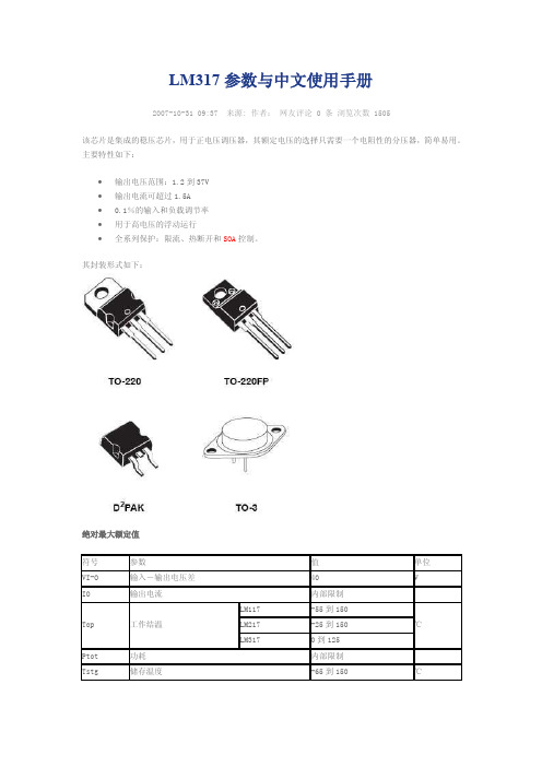
LM317参数与中文使用手册2007-10-31 09:37 来源: 作者:网友评论 0 条浏览次数 1505该芯片是集成的稳压芯片,用于正电压调压器,其额定电压的选择只需要一个电阻性的分压器,简单易用。
主要特性如下:∙输出电压范围:1.2到37V∙输出电流可超过1.5A∙0.1%的输入和负载调节率∙用于高电压的浮动运行∙全系列保护:限流、热断开和SOA控制。
其封装形式如下:绝对最大额定值引脚图(顶视)注:输入至少要比输出高2V,否则不能调压。
输入电要最高不能超过40V吧。
输出电流最好不超过1A。
输入12V的话,输出最高就是10V左右。
由于它内部还是线性稳压,因此功耗比较大。
当输入输入电压差比较大且输出电流也比较大时,注意317的功耗不要过大。
一般加散热片后功耗也不超过20W。
因此压差大时建议分档调压。
应用电路下面是赠送的两篇散文欣赏,可以仔细阅读,不需要的朋友可以下载后编辑删除!!谢谢!!脚下的时光不知走过多少地方,不知看过多少风景,不知听说过多少轶事;题记:蒲公英我走过很多地方,但是同样的,我也有更多的地方没去过!我渴望走遍地球上每一寸土地,我期许世界上每一个地方的人都善良!然而,现实的世界告诉我;理想的丰满一定要遇到拥有相同理想的另一半!我喜欢珠海,一个美丽的花园城市;我喜欢那里的天气,没有北方的寒冷;四季如春的温度感觉非常惬意,不用担心换季带来的差异!走在市区的街道上,绿化的花草树木被园丁修剪的井然有序;形态各异的花卉搭配得格外美观!尤其是除过草之后的绿地,泥土的芬芳与绿草的清新扑鼻而来,有一种身处大草原的感觉,使人心旷神怡!我时常一个人发呆,散步;看着过往的人群,车水马龙的街道;也时常去繁华的街巷,拥挤的商业中心;感觉这才是生活,正因为世界有了这么多事物的陪伴,才使我有了对美好生活的向往与喜悦!珠海的夜,很美;到处灯红酒绿,一派歌舞升平的祥和;每当夜幕降临,才是广东因有的生活的开始!溜冰场,酒吧,迪厅,大排档等等等等;我很庆幸在这里认识了很多人,他们教会了我很多,也帮助了我很多;我们都是来自五湖四海,为了同一个目标而聚集在一起的年轻人;我们时常出去聚会,嗨皮;但等到散场后,又回到了应有的孤寂!白天,可以去渔女,公园,九州城,免税店等等都是不错的地方!人常说,一个时代会有一个时代的代表;而我在这个曾经为之奋斗的地方,也时常会想起曾经相识的人,走过的地方,看过的风景;有时候,听着当时的流行歌曲,也会感伤;也会自嘲一笑;还有那公车到站的粤语提醒,还有那想见却永远没见的人;一篇篇,一幕幕久久回荡在脑海;早晨的肠粉,中午的餐饭,下午的炒粉,晚上的烧烤;好像味道还回味在口中一样!人,只有在对自己真诚的人的眼里,才会感觉到亲切;而我,也着实喜欢这座城市带给我家一样的温暖感觉!在这短暂而悠长的时光里,我成长了很多,也磨砺了很多;正是因为思想的成熟,阅历的增长,我选择了离开;去寻找属于自己的新的天地,新的开始,新的征程!其实,无论走过多少地方;都不重要!重要的是你从中得到什么!知识!阅历!思想!······每个人,在人生的道路上;难免遇到挫折困苦,也难免会因为一些因素而错失机缘!也不可能因为一时的过失而自暴自弃颓废一生!人,应该用豁达的心态来迎接下一秒的新鲜时光;而不是沉溺在上一秒的懊恼当中!每个人的路,都在自己的脚下;只有自己醒悟才能把未来的路走好,反之只会让错误延续到未来,从而影响以后的健康生活!即便曾经的时光再美好,那也只是人生道路上的一段插曲;没必要去纠结当时的愕然,愚昧!就像我,从来不对上一秒的事情产生情绪一样!一切都是恬淡的样子,顺其自然比什么都好!对于未来,只要真诚的去善待身边的所有;我相信,未来的时光,也该是你想象的模样!蒲公英2015.12.13家乡的茶籽林家乡高才坂,一年四季茶籽林郁郁葱葱,枝繁叶茂。
LM317功能说明
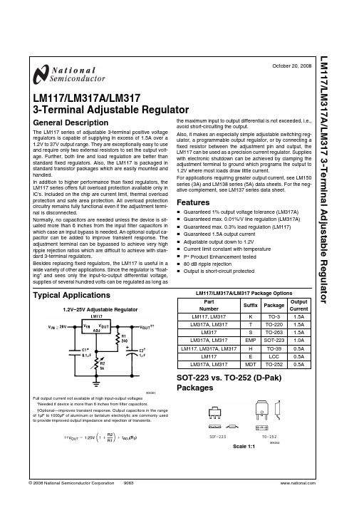
SOT-223 vs. TO-252 (D-Pak) Packages
Scale 1:1
906354
© 2008 National Semiconductor Corporation 9063
LM117/LM317A/LM317
Connection Diagrams
1.5A
SOT-223 4- Lead
0°C ≤ TJ ≤ +125°C −40°C ≤ TJ ≤ +125°C
TO-39 Metal Can
(H)
LCC
−55°C ≤ TJ ≤ +150°C −55°C ≤ TJ ≤ +150°C −40°C ≤ TJ ≤ +125°C 0°C ≤ TJ ≤ +125°C −55°C ≤ TJ ≤ +150°C
Package Marking LM117K STEEL P+ LM317K STEEL P+ LM117K/883 LM317AT P+ LM317T P+
LM317S P+
N01A
N07A
LM117H P+ LM117H/883 LM317AH P+ LM317H P+ LM117E/883
LM317MDT
TO-252 3- Lead D-Pack
0°C ≤ TJ ≤ +125°C −40°C ≤ TJ ≤ +125°C
1.0A
1.0A 0.5A 0.5A 0.5A 0.5A 0.5A 0.5A
0.5A
Order Number LM117K STEEL LM317K STEEL LM117K/883 LM317AT LM317T LM317S LM317SX LM317EMP LM317EMPX LM317AEMP LM317AEMPX LM117H LM117H/883 LM317AH LM317H LM117E/883 LM317MDT LM317MDTX LM317AMDT LM317AMDTX
LM317中英文资料
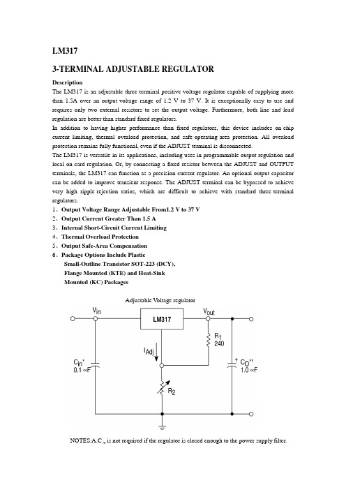
LM3173-TERMINAL ADJUSTABLE REGULATORDescriptionThe LM317 is an adjustable three-terminal positive-voltage regulator capable of supplying more than 1.5A over an output-voltage range of 1.2 V to 37 V. It is exceptionally easy to use and requires only two external resistors to set the output voltage. Furthermore, both line and load regulation are better than standard fixed regulators.In addition to having higher performance than fixed regulators, this device includes on-chip current limiting, thermal overload protection, and safe-operating-area protection. All overload protection remains fully functional, even if the ADJUST terminal is disconnected.The LM317 is versatile in its applications, including uses in programmable output regulation and local on-card regulation. Or, by connecting a fixed resistor between the ADJUST and OUTPUT terminals, the LM317 can function as a precision current regulator. An optional output capacitor can be added to improve transient response. The ADJUST terminal can be bypassed to achieve very high ripple-rejection ratios, which are difficult to achieve with standard three-terminal regulators.1、Output Voltage Range Adjustable From1.2 V to 37 V2、Output Current Greater Than 1.5 A3、Internal Short-Circuit Current Limiting4、Thermal Overload Protection5、Output Safe-Area Compensation6、Package Options Include PlasticSmall-Outline Transistor SOT-223 (DCY),Flange Mounted (KTE) and Heat-SinkMounted (KC) PackagesAdjustable V oltage regulatorNOTES:A.Cis not required if the regulator is closed enough to the power-supply filter.inB.Coimproves transient response, but is not needed for stability.Vout is calculated as Vout=Vref(1+12RR)+(IAdj×R2)APPLICATION INFORMATIONBasic Circuit OperationThe LM317 is a 3−terminal floating regulator. In operation, the LM317 develops and maintains a nominal 1.25 V reference (Vref) between its output and adjustment terminals. This reference voltage is converted to a programming current (IPROG) by R1 (see Figure 17), and this constant current flows through R2 to ground. The regulated output voltage is given by:Vout =Vref(1+12RR)+(IAdj×R2)Since the current from the adjustment terminal (IAdj) represents an error term in the equation, theLM317 was designed to control IAdjto less than 100 A and keep it constant. To do this, all quiescent operating current is returned to the output terminal. This imposes the requirement for a minimum load current. If the load current is less than this minimum, the output voltage will rise. Since the LM317 is a floating regulator, it is only the voltage differential across the circuit which is important to performance, and operation at high voltages with respect to ground is possible.Basic Circuit ConfigurationVref=1.25V TypicalLoad RegulationThe LM317 is capable of providing extremely good load regulation, but a few precautions are needed to obtain maximum performance. For best performance, the programming resistor (R1) should be connected as close to the regulator as possible to minimize line drops which effectively appear in series with the reference, thereby degrading regulation. The ground end of R2 can be returned near the load ground to provide remote ground sensing and improve load regulation.External CapacitorsA 0.1 μF disc or 1.0 μF tantalum input bypass capacitor (Cin) is recommended to reduce the sensitivity to input line impedance. The adjustment terminal may be bypassed to ground toimprove ripple rejection. This capacitor (CAdj) prevents ripple from being amplified as the output voltage is increased. A 10 μF capacitor should improve ripple rejection about 15 dB at 120 Hz in a 10 V application. Although the LM317 is stable with no output capacitance, like any feedback circuit, certain values of external capacitance can cause excessive ringing. An output capacitance(Co) in the form of a 1.0 μF tantalum or 25 μF aluminum electrolytic capacitor on the output swamps this effect and insures stability.Protection DiodesWhen external capacitors are used with any IC regulator it is sometimes necessary to add protection diodes to prevent the capacitors from discharging through low current points into the regulator. Figure 18 shows the LM317 with the recommended protection diodes for outputvoltages in excess of 25 V or high capacitance values (Co > 25 μF, CAdj> 10 μF). Diode D1prevents Cofrom discharging thru the IC during an input short circuit. Diode D2 protects againstcapacitor CAdjdischarging through the IC during an output short circuit. The combination ofdiodes D1 and D2 prevents CAdjfrom discharging through the IC during an input short circuit. Voltage Regulator with Protection DiodesLM317—三端可调节输出正电压稳压器概述LM317是3端可调节输出正电压稳压器,在输出范围为1.2V到37V范围时能提供超过1.5A的电流。
LM317参数与中文使用手册
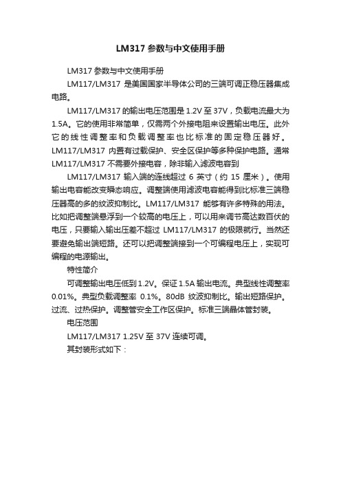
LM317参数与中文使用手册LM317参数与中文使用手册LM117/LM317 是美国国家半导体公司的三端可调正稳压器集成电路。
LM117/LM317 的输出电压范围是1.2V至37V,负载电流最大为1.5A。
它的使用非常简单,仅需两个外接电阻来设置输出电压。
此外它的线性调整率和负载调整率也比标准的固定稳压器好。
LM117/LM317 内置有过载保护、安全区保护等多种保护电路。
通常LM117/LM317 不需要外接电容,除非输入滤波电容到LM117/LM317 输入端的连线超过 6 英寸(约 15 厘米)。
使用输出电容能改变瞬态响应。
调整端使用滤波电容能得到比标准三端稳压器高的多的纹波抑制比。
LM117/LM317能够有许多特殊的用法。
比如把调整端悬浮到一个较高的电压上,可以用来调节高达数百伏的电压,只要输入输出压差不超过LM117/LM317的极限就行。
当然还要避免输出端短路。
还可以把调整端接到一个可编程电压上,实现可编程的电源输出。
特性简介可调整输出电压低到1.2V。
保证1.5A 输出电流。
典型线性调整率0.01%。
典型负载调整率0.1%。
80dB 纹波抑制比。
输出短路保护。
过流、过热保护。
调整管安全工作区保护。
标准三端晶体管封装。
电压范围LM117/LM317 1.25V 至 37V 连续可调。
其封装形式如下:符号参数值单位VI-O 输入-输出电压差40 VIO 输出电流内部限制Top 工作结温LM117 -55到150 ℃LM217 -25到150 LM317 0到125Ptot 功耗内部限制Tstg 储存温度-65到150 ℃引脚图(顶视)注:输入至少要比输出高2V,否则不能调压。
输入电要最高不能超过40V吧。
输出电流最好不超过1A。
输入12V的话,输出最高就是10V 左右。
由于它内部还是线性稳压,因此功耗比较大。
当输入输入电压差比较大且输出电流也比较大时,注意317的功耗不要过大。
一般加散热片后功耗也不超过20W。
lm317可调稳压管(中文资料)

lm317中文资料|lm317应用电路图|LM317 pdf内容介绍:包含了LM317的各种应用电路图资料,LM317的工作原理资料,LM317的中文PDF资料,LM317的英文PDF资料,LM317的引脚(管脚)图.
LM317工作原理:LM317的输入最同电压为30多伏,输出电压1.5----32V...电流1.5A...不过在用的时候要注意功耗问题...注意散热问题。
LM317有三个引脚.一个输入一个输出一个电压调节。
输入引脚输入正电压,输出引脚接负载, 电压调节引脚一个引脚接电阻(200左右)在输出引脚,另一个接可调电阻(几K)接于地.输入和输出引脚对地要接滤波电容.
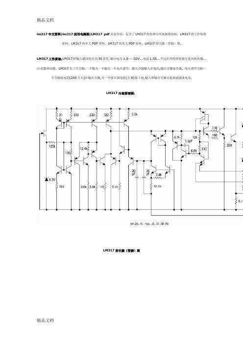
LM317内部原理图:
LM317的引脚(管脚)图
LM317应用电路图:1.LM317标准应用电路图
2.LM317带可调限流和输出电压的标准应用电路图
3. LM317的5.0V电子关断稳压器应用电路图
4.LM317电流稳压器应用电路图
5.LM317可调节电流限流器的应用电路图
6. LM317软启动应用电路图。
LM317M-D(LDO)
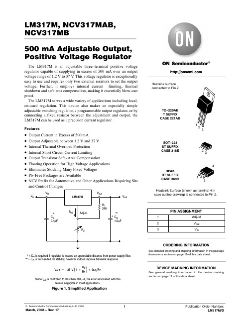
Figure Symbol
Min
Typ
Max
Unit
Line Regulation (Note 3) (TA = 25°C, 3.0 V ≤ VI - VO ≤ 40 V)
Load Regulation (Note 3) ăTA = 25°C, 10 mA ≤ IO ≤ 0.5 A ąVO ≤ 5.0 V ąVO ≥ 5.0 V
Figure 1. Simplified Application
ORDERING INFORMATION
See detailed ordering and shipping information in the package dimensions section on page 10 of this data sheet.
and Control Changes
Vin Vin
Vout
LM317M
Vout
* Cin 0.1mF
IAdj Adjust
R1 240
** + CO
1.0mF
R2
Heatsink surface connected to Pin 2
TO-220AB T SUFFIX CASE 221AB
SOT-223 ST SUFFIX CASE 318E
1 2 3 1 23
DPAK DT SUFFIX CASE 369C
4
12 3
Heatsink Surface (shown as terminal 4 in case outline drawing) is connected to Pin 2.
PD
Internally Limited
qJA
LM317L规格书

O
I
ELECTRICAL CHARACTERRISTISTICS
PARAMETER Line Regulation Load Regulation Reference Voltage Adjustment Pin Current Adjustment Pin Current Change Minimum Load Current Current Limit RMS Output Noise % of VOUT Ripple Rejection Ratio
MINΒιβλιοθήκη TYP 0.02 0.3 1.25 50 0.2 3.5 1.5 200 50 0.03 65 80
MAX 0.07 1.5 1.30 100 5 5 2.5 300 120
UNIT %/V % V µA µA mA mA % dB
1.20
90 25 58
Unless otherwise noted, these specifications apply: 0℃≦TJ≦70℃ for the WS317L;VIN-VOUT=5V and IOUT= 40mA. Although power dissipation is internally limited, these specifications are applicable for power dissipation up to 625mW. IMAX is 100mA Regulation is measure at constant junction temperature, using pulse testing with a low duty cycle. Changes in output voltage due to heating effects are covered under the specification for thermal regulation. Thermal resistance of the TO-92 package is 180℃/W junction to ambient with 0.4” leads from a PC board and 160 ℃/W junction to ambient with 0.125” length to a PC board
LM317全球某工商大学版中文资料

LM317By Cl1.概述LM117/LM317是美国国家半导体公司的三端可调正稳压器集成电路。
Adj调整端和输出端out提供一个内部参考电压1.25V。
输出端范围是1.2V至37V,负载最大电流为1.5A。
使用简单,只需两个外接电阻来设置输出电压。
它的线性调整率和负载调整率也比标准的固定稳压器好。
内置过载保护,安全区保护等多种保护电路。
2.封装2.1.TO-92底视图3. 片内原理图4. 应用4.1. 标准应用如果输入Vin=5V ,Vout 要求输出3.3V 左右,R1=240Ω,则:忽略Iadj ,6.393240)125.13.3(1)1(2=⨯-=⨯-=R V Vo R REF经过240Ω扥电阻的电流为1.25V/240Ω=5.2083mA实际情况下,R1如果选2个470Ω并联,为235Ω,那么,R2=200+200=400Ω,那么,Vout=1.25V(1+400/235)=3.377V通常LM117/LM317不需要外接电容,除非输入滤波电容到输入端的连接线超过6英寸(约15厘米)。
使用输出电容对稳定性而言不需要,但能改变瞬态响应。
调整端使用滤波电容能得到比标准三端稳压器高得多的纹波抑制比。
5.参数5.1.电气特征(Vi - Vo = 5 V, Io = 500 mA, IMAX = 1.5A and PMAX = 20W, unless otherwise specified)(*) CADJ is connected between pin 1 and ground.Note:(1) Unless otherwise specified the above specs, apply over the following conditions : LM 117 Tj = – 55 to 150°C;LM 217 Tj = – 25 to 150°C ; LM 317 Tj = 0 to 125°C.。
LM317L
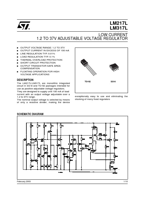
TEST CIRCUIT
2/10
LM217L/LM317L
ELECTRICAL CHARACTERISTICS OF LM217L (refer to the test circuits, TJ = - 40 to 125°C, VI - VO = 5 V, IO = 40 mA, unless otherwise specified).
4/10
LM217L/LM317L
Figure 4 : Voltage Regulator with Protection Diodes
Figure 5 : Slow Turn-on 15V Regulator
Figure 6 : Current Regulator
Vref 1.25V IO = + IADJ ≈ R1 R1
CONNECTION DIAGRAM (top view)
PIN 1 = ADJUST PIN 2 = IN PIN 3 = OUT
BOTTOM VIEW
SO-8
TO-92
ORDERING CODES
TYPE LM217L LM317L SO-8 LM217LD LM317LD TO-92 LM217LZ LM317LZ
TO-92 SO-8
DESCRIPTION The LM217L/LM317L are monolithic integrated circuit in SO-8 and TO-92 packages intended for use as positive adjustable voltage regulators. They are designed to supply until 100 mA of load current with an output voltage adjustable over a 1.2 to 37V range. The nominal output voltage is selected by means of only a resistive divider, making the device
LM317_DataSheet
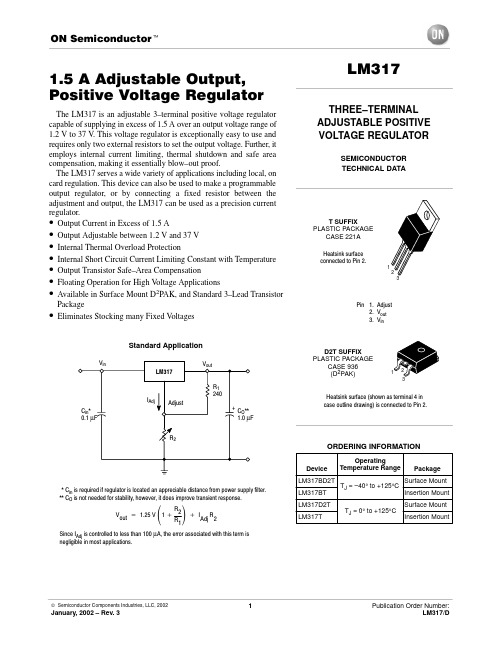
R2
**ĂCin is required if regulator is located an appreciable distance from power supply filter. **ĂCO is not needed for stability, however, it does improve transient response.
1.25
0.02
20 0.3 0.7 3.5
2.2 0.4 0.003
65 80 0.3
0.04
%/V
25
mV
0.5
% VO
0.07
% VO/W
100
µA
5.0
µA
1.3
V
0.07
%V
70
mV
1.5
% VO
–
% VO
10
mA
A – –
–
% VO
dB – –
1.0
%/1.0 k
Hrs.
Thermal Resistance Junction to Case, T Package
RθJC
–
5.0
–
°C/W
NOTES: 1. Tlow to Thigh = 0° to +125°C, for LM317T, D2T. Tlow to Thigh = –40° to +125°C, for LM317BT, BD2T. 2. Imax = 1.5 A, Pmax = 20 W 3. Load and line regulation are specified at constant junction temperature. Changes in VO due to heating effects must be taken into account separately. Pulse testing with low duty cycle is used.
LM317MDTG中文资料

PD
Internally Limited
qJA
70
°C/W
qJC
5.0
°C/W
ąąTA = 25°C ąąąThermal Resistance, Junction-to-Air ąąąThermal Resistance, Junction-to-Case ąPlastic Package, ST Suffix, Case 318E
Figure 1. Simplified Application
ORDERING INFORMATION
See detailed ordering and shipping information in the package dimensions section on page 10 of this data sheet.
Line Regulation 3.0 V ≤ VI-VO ≤ 40 V (Note 3)
Load Regulation 10 mA ≤ IO ≤ 0.5 A (Note 3) ąVO ≤ 5.0 V ąVO ≥ 5.0 V
Temperature Stability (Tlow ≤ TJ ≤ Thigh)
Ripple Rejection, VO = 10 V, f = 120 Hz (Note 4) ăWithout CAdj ăCAdj = 10 mF
Thermal Shutdown (Note 5)
3
Regline
4
Regload
5
IAdj
3, 4
DIAdj
5
Vref
3
Regline
4
Regload
ELECTRICAL CHARACTERISTICS (VI - VO = 5.0 V; IO = 0.1 A, TJ = Tlow to Thigh (Note 2), unless otherwise noted.)
ST LM217M LM317M 数据手册
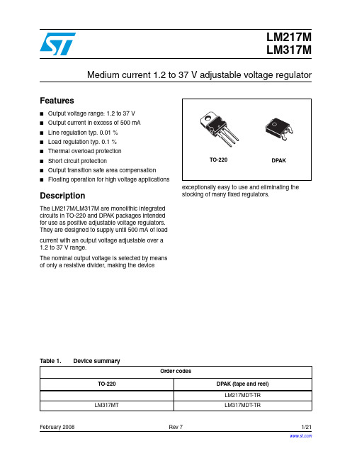
February 2008Rev 71/21LM217M LM317MMedium current 1.2 to 37 V adjustable voltage regulatorFeatures■Output voltage range: 1.2 to 37 V ■Output current in excess of 500 mA ■Line regulation typ. 0.01 %■Load regulation typ. 0.1 %■Thermal overload protection ■Short circuit protection■Output transition safe area compensation ■Floating operation for high voltage applicationsDescriptionThe LM217M/LM317M are monolithic integrated circuits in TO-220 and DPAK packages intended for use as positive adjustable voltage regulators. They are designed to supply until 500 mA of load current with an output voltage adjustable over a 1.2 to 37 V range.The nominal output voltage is selected by means of only a resistive divider, making the deviceexceptionally easy to use and eliminating the stocking of many fixed regulators.Table 1.Device summaryOrder codesTO-220DPAK (tape and reel)LM217MDT -TRLM317MTLM317MDT -TRContents LM217M - LM317MContents1Diagram . . . . . . . . . . . . . . . . . . . . . . . . . . . . . . . . . . . . . . . . . . . . . . . . . . . 3 2Pin configuration . . . . . . . . . . . . . . . . . . . . . . . . . . . . . . . . . . . . . . . . . . . 4 3Maximum ratings . . . . . . . . . . . . . . . . . . . . . . . . . . . . . . . . . . . . . . . . . . . . 5 4Electrical characteristics . . . . . . . . . . . . . . . . . . . . . . . . . . . . . . . . . . . . . 6 5Typical performance . . . . . . . . . . . . . . . . . . . . . . . . . . . . . . . . . . . . . . . . . 86Application information . . . . . . . . . . . . . . . . . . . . . . . . . . . . . . . . . . . . . . 96.1External capacitors (Figure8) . . . . . . . . . . . . . . . . . . . . . . . . . . . . . . . . . . 96.2Protection diodes (Figure8) . . . . . . . . . . . . . . . . . . . . . . . . . . . . . . . . . . . . 96.3Start-up block . . . . . . . . . . . . . . . . . . . . . . . . . . . . . . . . . . . . . . . . . . . . . . . 9 7Application circuits . . . . . . . . . . . . . . . . . . . . . . . . . . . . . . . . . . . . . . . . . 10 8Package mechanical data . . . . . . . . . . . . . . . . . . . . . . . . . . . . . . . . . . . . 12 9Revision history . . . . . . . . . . . . . . . . . . . . . . . . . . . . . . . . . . . . . . . . . . . 202/21LM217M - LM317M Diagram 1 Diagram3/21Pin configuration LM217M - LM317M 2 Pin configuration4/21LM217M - LM317M Maximum ratings5/213 Maximum ratingsTable 2.Absolute maximum ratingsSymbol ParameterValue Unit V I -V O Input-output differential voltage 40V P D Power dissipationInternally limited mW T OP Operating junction temperature range (1)1.Re-Boot is not guaranteed for T J ≥ 85°C.for LM217M -40 to 125°C for LM317M0 to 125T STGStorage temperature range-55 to 150°CTable 3.Thermal dataSymbol ParameterTO-220DPAK Unit R thJC Thermal resistance junction-case 38°C/W R thJAThermal resistance junction-ambient50100°C/WElectrical characteristics LM217M - LM317M6/214 Electrical characteristicsTable 4.Electrical characteristics of LM217M (refer to the test circuits, T J = - 40 to 125 °C,V I - V O = 5 V, I O = 100 mA, P D ≤ 7.5 W, unless otherwise specified)Symbol ParameterTest conditionsMin.Typ.Max.Unit ΔV OLine regulationV I - V O = 3 to 40 V T J = 25°C0.010.02%/V0.020.05ΔV OLoad regulationV O ≤ 5 VI O = 10 to 500mAT J = 25°C515mV2050V O ≥ 5 VI O = 10 to 500mAT J = 25°C0.10.3%/V O 0.31I ADJ Adjustment pin current 50100µA ΔI ADJ Adjustment pin current V I - V O = 3 to 40 V, I O = 10 to 500 mA 0.25µA V REF Reference voltage V I - V O = 3 to 40 V, I O = 10 to 500 mA1.21.25 1.3V ΔV O /V O Output voltagetemperature stability 0.7%I O(min)Minimum load current V I - V O = 40 V 3.55mA I O(max)Maximum output current V I - V O ≤ 15 V5001000mA V I - V O = 40 V , P d < P DMAX , T J = 25°C 200eN Output noise voltage (percentage of V O ) B = 10 Hz to 100 kHz, T J = 25°C 0.003%SVRSupply voltage rejection (1)1.C ADJ is connected between Adjust pin and Ground.T J = 25°C f = 120 HzC ADJ = 065dBC ADJ = 10 µF6680LM217M - LM317M Electrical characteristics7/21Table 5.Electrical characteristics of LM317M (refer to the test circuits, T J = 0 to 125 °C,V I - V O = 5 V, I O = 100 mA, P D ≤ 7.5 W, unless otherwise specified)Symbol ParameterTest conditionsMin.Typ.Max.Unit ΔV OLine regulationV I - V O = 3 to 40 V T J = 25°C0.010.04%/V0.020.07ΔV OLoad regulationV O ≤ 5 VI O = 10 to 500mAT J = 25°C525mV2070V O ≥ 5 VI O = 10 to 500mAT J = 25°C0.10.5%/V O 0.3 1.5I ADJ Adjustment pin current 50100µA ΔI ADJ Adjustment pin current V I - V O = 3 to 40 V, I O = 10 to 500 mA 0.25µA V REF Reference voltage V I - V O = 3 to 40 V, I O = 10 to 500 mA1.21.25 1.3V ΔV O /V O Output voltagetemperature stability 0.7%I O(min)Minimum load current V I - V O = 40 V 3.510mA I O(max)Maximum output current V I - V O ≤ 15 V5001000mA V I - V O = 40 V , P d < P DMAX , T J = 25°C 200eN Output noise voltage (percentage of V O ) B = 10 Hz to 100 kHz, T J = 25°C 0.003%SVRSupply voltage rejection (1)T J = 25°C f = 120 HzC ADJ = 065dBC ADJ = 10 µF66801.C ADJ is connected between Adjust pin and Ground.Typical performance LM217M - LM317M8/215 Typical performanceNote:P dmax calculated for T a = 50°C.LM217M - LM317M Application information9/216 Application informationThe LM217M/LM317M provide an internal reference voltage of 1.25 V between the outputand adjustment terminals. These devices are used to set a constant current flow across an external resistor divider (see Figure 6), giving an output voltage V O of: V O = V REF (1 + R 2 / R 1) + I ADJ R 2.The devices were designed to minimize the term I ADJ (100 µA max) and to maintain it very constant in line and load changes. Usually, the error term I ADJ × R 2 can be neglected. To obtain the previous requirement, all the regulator quiescent current is returned to the output terminal, imposing a minimum load current condition. If the load is insufficient, the output voltage will rise.Since the LM217M/LM317M devices are floating regulators and "see" only the input-to-output differential voltage, supplies of very high voltage with respect to ground can beregulated as long as the maximum input-to-output differential is not exceeded. Furthermore, programmable regulators are easily obtained and, by connecting a fixed resistor between the adjustment and output, the devices can be used as a precision current regulator. In order to optimize the load regulation, the current set resistor R 1 (see Figure 6) should be tied as close as possible to the regulator, while the ground terminal of R 2 should be near the ground of the load to provide remote ground sensing.6.1 External capacitors (Figure 8)Normally no capacitors are needed unless the devices are situated far from the input filter capacitors; in which case an input bypass is needed.A 0.1 µF disc or 1 µF tantalum input bypass capacitor (C I ) is recommended to reduce the sensitivity to input line impedance.The adjustment terminal may be bypassed to ground to improve ripple rejection. Thiscapacitor (C ADJ ) prevents ripple from being amplified as the output voltage is increased. A 10 µF capacitor should improve ripple rejection of about 80 dB at 120 Hz in a 10 V application.Although the LM217M/LM317M devices are stable with no output capacitance like any feedback circuit, certain values of external capacitance can cause excessive ringing. An output capacitance (C O ) in the form of a 1 µF tantalum or 25 µF aluminium electrolytic capacitor on the output swamps this effect and insures stability.6.2 Protection diodes (Figure 8)When external capacitors are used with any IC regulator it is sometimes necessary to add protection diodes to prevent the capacitors from discharging through low current points into the regulator.Figure 6 shows the LM217M/LM317M with the recommended protection diodes for output voltages in excess of 25 V or high capacitance values (C 3 > 25 µF , C 2 > 10 µF). Diode D1 prevents C 3 from discharging through the IC during an input short-circuit. The combination of diodes D1 and D2 prevents C 2 from discharging through the regulator during an input or output short-circuit.6.3 Start-up blockIt’s not guaranteed the Re-Boot of the device when the junction temperature is over 85 °C.Application circuits LM217M - LM317M10/217 Application circuitsFigure 8.Voltage regulator with protection diodesFigure 9.Slow turn-on 15 V regulatorFigure 10.Current regulatorI O =V REF /R 1 + I ADJ = 1.25V/R 1LM217M - LM317MApplication circuitsFigure 11.5 V electronic shut-down regulatorFigure 12.Digitally selected outputs(R 2 = sets maximum V O )Package mechanical data LM217M - LM317M 8 Package mechanical dataIn order to meet environmental requirements, ST offers these devices in ECOPACK®packages. These packages have a lead-free second level interconnect. The category ofsecond Level Interconnect is marked on the package and on the inner box label, incompliance with JEDEC Standard JESD97. The maximum ratings related to solderingconditions are also marked on the inner box label. ECOPACK is an ST trademark.ECOPACK specifications are available at: .LM217M - LM317M Package mechanical dataPackage mechanical data LM217M - LM317MLM217M - LM317M Package mechanical dataPackage mechanical data LM217M - LM317MLM217M - LM317M Package mechanical dataNote:The DPAK package coming from the two subcontractors (Fujitsu and IDS) are fully compatible with the ST's package suggested footprint.Table 6.DPAK mechanical dataDim.type STD-STtype FUJITSU-Subcon.type IDS-Subconmm.mm.mm.Min.Typ.Max.Min.Typ.Max.Min.Typ.Max.A 2.20 2.40 2.25 2.302.35 2.19 2.38A10.90 1.100.96 1.060.89 1.14A20.030.2300.100.030.23b 0.640.900.760.860.640.88b4 5.20 5.40 5.28 5.38 5.21 5.46c 0.450.600.460.560.460.58c20.480.600.460.560.460.58D 6.006.206.05 6.15 5.976.22D1 5.105.27 5.47 5.20E 6.406.606.556.60 6.656.356.73E1 4.70 4.77 4.70e 2.282.232.282.332.28e1 4.40 4.60 4.51 4.61H 9.3510.109.9010.309.4010.42L 1.001.401.600.90L1 2.80 2.50 2.65L20.801.03 1.130.89 1.27L40.601.000.700.900.641.02R 0.200.400.20V20°8°0°8°0°8°Package mechanical data LM217M - LM317M Figure 16.DPAK footprint recommended dataTable 7.Footprint dataValuesDim.mm.inch.A 6.700.264B 6.700.64C 1.80.070D 3.00.118E 1.600.063F 2.300.091G 2.300.091LM217M - LM317M Package mechanical dataRevision history LM217M - LM317M 9 Revision historyTable 8.Document revision historyDate Revision Changes21-Jun-20045The document has been reformatted.06-Dec-20066DP AK mechanical data updated, added footprint data.11-Feb-20087Added: Table1 on page1.LM217M - LM317MPlease Read Carefully:Information in this document is provided solely in connection with ST products. STMicroelectronics NV and its subsidiaries (“ST”) reserve the right to make changes, corrections, modifications or improvements, to this document, and the products and services described herein at any time, without notice.All ST products are sold pursuant to ST’s terms and conditions of sale.Purchasers are solely responsible for the choice, selection and use of the ST products and services described herein, and ST assumes no liability whatsoever relating to the choice, selection or use of the ST products and services described herein.No license, express or implied, by estoppel or otherwise, to any intellectual property rights is granted under this document. If any part of this document refers to any third party products or services it shall not be deemed a license grant by ST for the use of such third party products or services, or any intellectual property contained therein or considered as a warranty covering the use in any manner whatsoever of such third party products or services or any intellectual property contained therein.UNLESS OTHERWISE SET FORTH IN ST’S TERMS AND CONDITIONS OF SALE ST DISCLAIMS ANY EXPRESS OR IMPLIED WARRANTY WITH RESPECT TO THE USE AND/OR SALE OF ST PRODUCTS INCLUDING WITHOUT LIMITATION IMPLIED WARRANTIES OF MERCHANTABILITY, FITNESS FOR A PARTICULAR PURPOSE (AND THEIR EQUIVALENTS UNDER THE LAWS OF ANY JURISDICTION), OR INFRINGEMENT OF ANY PATENT, COPYRIGHT OR OTHER INTELLECTUAL PROPERTY RIGHT. UNLESS EXPRESSLY APPROVED IN WRITING BY AN AUTHORIZED ST REPRESENTATIVE, ST PRODUCTS ARE NOT RECOMMENDED, AUTHORIZED OR WARRANTED FOR USE IN MILITARY, AIR CRAFT, SPACE, LIFE SAVING, OR LIFE SUSTAINING APPLICATIONS, NOR IN PRODUCTS OR SYSTEMS WHERE FAILURE OR MALFUNCTION MAY RESULT IN PERSONAL INJURY, DEATH, OR SEVERE PROPERTY OR ENVIRONMENTAL DAMAGE. ST PRODUCTS WHICH ARE NOT SPECIFIED AS "AUTOMOTIVE GRADE" MAY ONLY BE USED IN AUTOMOTIVE APPLICATIONS AT USER’S OWN RISK.Resale of ST products with provisions different from the statements and/or technical features set forth in this document shall immediately void any warranty granted by ST for the ST product or service described herein and shall not create or extend in any manner whatsoever, any liability of ST.ST and the ST logo are trademarks or registered trademarks of ST in various countries.Information in this document supersedes and replaces all information previously supplied.The ST logo is a registered trademark of STMicroelectronics. All other names are the property of their respective owners.© 2008 STMicroelectronics - All rights reservedSTMicroelectronics group of companiesAustralia - Belgium - Brazil - Canada - China - Czech Republic - Finland - France - Germany - Hong Kong - India - Israel - Italy - Japan - Malaysia - Malta - Morocco - Singapore - Spain - Sweden - Switzerland - United Kingdom - United States of America21/21。
NATIONAL SEMICONDUCTOR LM117HV LM317HV 说明书

LM117HV/LM317HV3-Terminal Adjustable RegulatorGeneral DescriptionThe LM117HV/LM317HV are adjustable 3-terminal positive voltage regulators capable of supplying in excess of 1.5A over a 1.2V to 57V output range.They are exceptionally easy to use and require only two external resistors to set the output voltage.Further,both line and load regulation are bet-ter than standard fixed regulators.Also,the LM117HV is packaged in standard transistor packages which are easily mounted and handled.In addition to higher performance than fixed regulators,the LM117HV series offers full overload protection available only in IC’s.Included on the chip are current limit,thermal over-load protection and safe area protection.All overload protec-tion circuitry remains fully functional even if the adjustment terminal is disconnected.Normally,no capacitors are needed unless the device is situ-ated more than 6inches from the input filter capacitors in which case an input bypass is needed.An optional output capacitor can be added to improve transient response.The adjustment terminal can be bypassed to achieve very high ripple rejections ratios which are difficult to achieve with standard 3-terminal regulators.Besides replacing fixed regulators,the LM117HV is useful in a wide variety of other applications.Since the regulator is “floating”and sees only the input-to-output differential volt-age,supplies of several hundred volts can be regulated as long as the maximum input to output differential is not ex-ceeded,i.e.do not short the output to ground.Also,it makes an especially simple adjustable switching regulator,a programmable output regulator,or by connecting a fixed resistor between the adjustment and output,the LM117HV can be used as a precision current regulator.Sup-plies with electronic shutdown can be achieved by clamping the adjustment terminal to ground which programs the out-put to 1.2V where most loads draw little current.The LM117HVK STEEL and LM317HVK STEEL are pack-aged in standard TO-3transistor packages,while the LM117HVH and LM317HVH are packaged in a solid Kovar base TO-39transistor package.The LM317HVT uses a TO-220plastic package.The LM117HV is rated for operation from −55˚C to +150˚C,and the LM317HV from 0˚C to +125˚C.Featuresn Adjustable output down to 1.2V n Guaranteed 1.5A output current n Line regulation typically 0.01%/V n Load regulation typically 0.1%n Current limit constant with temperature n 100%electrical burn-inn Eliminates the need to stock many voltages n Standard 3-lead transistor package n 80dB ripple rejectionn Output is short-circuit protected nP +Product Enhancement testedTypical Applications1.2V-45V Adjustable RegulatorDS009062-1Full output current not available at high input-output voltages†Optional —improves transient response.Output capacitors in the range of 1µF to 1000µF of aluminum or tantalum electrolytic are commonly used to provide improved output impedance and rejection of transients.*Needed if device is more than 6inches from filter capacitors.April 2000LM117HV/LM317HV 3-Terminal Adjustable Regulator©2000National Semiconductor Corporation Typical Applications(Continued)Digitally Selected OutputsDS009062-2*Sets maximum V OUT5V Logic Regulator with Electronic Shutdown *DS009062-3*Min.output ≈1.2VL M 117H V /L M 317H V 2Absolute Maximum Ratings(Note1)If Military/Aerospace specified devices are required, please contact the National Semiconductor Sales Office/ Distributors for availability and specifications.(Note4)Power Dissipation Internally limited Input—Output Voltage Differential+60V,−0.3V Operating Junction Temperature RangeLM117HV−55˚C to+150˚C LM317HV0˚C to+125˚C Storage Temperature−65˚C to+150˚C Lead Temperature(Soldering,10sec.)300˚C ESD Tolerance(Note5)2000VElectrical Characteristics(Note2)Parameter Conditions LM117HV LM317HV UnitsMin Typ Max Min Typ MaxLine Regulation T J=25˚C,3V≤V IN−V OUT≤60V0.010.020.010.04%/V(Note3)I L=10mALoad Regulation T J=25˚C,10mA≤I OUT≤I MAX0.10.30.10.5% Thermal Regulation T J=25˚C,20ms Pulse0.030.070.040.07%/W Adjustment Pin Current5010050100µA Adjustment Pin Current Change10mA≤I L≤I MAX0.250.25µA3.0V≤(V IN−V OUT)≤60VReference Voltage 3.0V≤(V IN−V OUT)≤60V,(Note4) 1.20 1.25 1.30 1.20 1.25 1.30V10mA≤I OUT≤I MAX,P≤P MAXLine Regulation 3.0V≤(V IN−V OUT)≤60V,0.020.050.020.07%/VI L=10mA,(Note3)Load Regulation10mA≤I OUT≤I MAX(Note3)0.310.3 1.5% Temperature Stability T MIN≤T J≤T MAX11% Minimum Load Current(V IN−V OUT)=60V 3.57 3.512mA Current Limit(V IN−V OUT)≤15VK,T Packages 1.5 2.2 3.5 1.5 2.2 3.7AH Package0.50.8 1.80.50.8 1.9A(V IN−V OUT)≤60VK,T Packages0.30.3AH Package0.030.03ARMS Output Noise,%of V OUT T J=25˚C,10Hz≤f≤10kHz0.0030.003%Ripple Rejection Ratio V OUT=10V,f=120Hz6565dBC ADJ=10µF66806680dBLong-Term Stability T J=125˚C0.310.31% Thermal Resistance,H Package12151215˚C/W Junction to Case T Package45˚C/WK Package 2.33 2.33˚C/W Thermal Resistance,H Package140140˚C/W Junction to Ambient T Package50˚C/W(no heat sink)K Package3535˚C/WNote1:“Absolute Maximum Ratings”indicate limits beyond which damage to the device may occur.Operating Ratings indicate conditions for which the device is functional,but do not guarantee specific performance limits.Note2:Unless otherwise specified,these specifications apply:−55˚C≤T J≤+150˚C for the LM117HV,and0˚C≤T J≤+125˚C for the LM317HV;V IN−V OUT=5V and I OUT=0.1A for the TO-39package and I OUT=0.5A for the TO-3and TO-220packages.Although power dissipation is internally limited,these specifications are applicable for power dissipations of2W for the TO-39and20W for the TO-3and TO-220.I MAX is1.5A for the TO-3and TO-220and0.5A for the TO-39package.Note3:Regulation is measured at constant junction temperature.Changes in output voltage due to heating effects must be taken into account separately.Pulse test-ing with low duty cycle is used.Note4:Refer to RETS117HVH for LM117HVH or RETS117HVK for LM117HVK military specificatioins.Note5:Human body model,1.5kΩin series with100pF.LM117HV/LM317HV3Typical Performance CharacteristicsOutput capacitor =0µF unless otherwise noted.Load RegulationDS009062-32Current LimitDS009062-33Adjustment CurrentDS009062-34Dropout Voltage DS009062-35Temperature Stability DS009062-36Minimum Operating CurrentDS009062-37Ripple Rejection DS009062-38Ripple Rejection DS009062-39Ripple RejectionDS009062-40Output Impedance DS009062-41Line Transient Response DS009062-42Load Transient ResponseDS009062-43L M 117H V /L M 317H V 4Application HintsIn operation,the LM117HV develops a nominal 1.25V refer-ence voltage,V REF ,between the output and adjustment ter-minal.The reference voltage is impressed across program resistor R1and,since the voltage is constant,a constant current I 1then flows through the output set resistor R2,giv-ing an output voltage ofSince the 100µA current from the adjustment terminal repre-sents an error term,the LM117HV was designed to minimize I ADJ and make it very constant with line and load changes.To do this,all quiescent operating current is returned to the output establishing a minimum load current requirement.If there is insufficient load on the output,the output will rise.External CapacitorsAn input bypass capacitor is recommended.A 0.1µF disc or 1µF solid tantalum on the input is suitable input bypassing for almost all applications.The device is more sensitive to the absence of input bypassing when adjustment or output capacitors are used but the above values will eliminate the possiblity of problems.The adjustment terminal can be bypassed to ground on the LM117HV to improve ripple rejection.This bypass capacitor prevents ripple from being amplified as the output voltage is increased.With a 10µF bypass capacitor 80dB ripple rejec-tion is obtainable at any output level.Increases over 10µF do not appreciably improve the ripple rejection at frequen-cies above 120Hz.If the bypass capacitor is used,it is sometimes necessary to include protection diodes to prevent the capacitor from discharging through internal low current paths and damaging the device.In general,the best type of capacitors to use are solid tanta-lum.Solid tantalum capacitors have low impedance even at high frequencies.Depending upon capacitor construction,it takes about 25µF in aluminum electrolytic to equal 1µF solid tantalum at high frequencies.Ceramic capacitors are also good at high frequencies;but some types have a large decrease in capacitance at frequencies around 0.5MHz.For this reason,0.01µF disc may seem to work better than a 0.1µF disc as a bypass.Although the LM117HV is stable with no output capacitors,like any feedback circuit,certain values of external capaci-tance can cause excessive ringing.This occurs with values between 500pF and 5000pF.A 1µF solid tantalum (or 25µF aluminum electrolytic)on the output swamps this effect andinsures stability.Any increase of load capacitance larger than 10µF will merely improve the loop stability and output impedance.Load RegulationThe LM117HV is capable of providing extremely good load regulation but a few precautions are needed to obtain maxi-mum performance.The current set resistor connected be-tween the adjustment terminal and the output terminal (usu-ally 240Ω)should be tied directly to the output of the regulator rather than near the load.This eliminates line drops from appearing effectively in series with the reference and degrading regulation.For example,a 15V regulator with 0.05Ωresistance between the regulator and load will have a load regulation due to line resistance of 0.05Ωx I L .If the set resistor is connected near the load the effective line resis-tance will be 0.05Ω(1+R2/R1)or in this case,11.5times worse.Figure 2shows the effect of resistance between the regula-tor and 240Ωset resistor.With the TO-3package,it is easy to minimize the resistance from the case to the set resistor,by using two separate leads to the case.However,with the TO-5package,care should be taken to minimize the wire length of the output lead.The ground of R2can be returned near the ground of the load to provide remote ground sensing and improve load regulation.Protection DiodesWhen external capacitors are used with any IC regulator it is sometimes necessary to add protection diodes to prevent the capacitors from discharging through low current points into the regulator.Most 10µF capacitors have low enough internal series resistance to deliver 20A spikes when shorted.Although the surge is short,there is enough energy to damage parts of the IC.When an output capacitor is connected to a regulator and the input is shorted,the output capacitor will discharge into the output of the regulator.The discharge current depends on the value of the capacitor,the output voltage of the regu-lator,and the rate of decrease of V IN .In the LM117HV,this discharge path is through a large junction that is able to sus-tain 15A surge with no problem.This is not true of other types of positive regulators.For output capacitors of 25µF or less,there is no need to use diodes.The bypass capacitor on the adjustment terminal can dis-charge through a low current junction.Discharge occurs when either the input or output is shorted.Internal to the LM117HV is a 50Ωresistor which limits the peak discharge current.No protection is needed for output voltages of 25VDS009062-5FIGURE 1.DS009062-6FIGURE 2.Regulator with Line Resistance in Output LeadLM117HV/LM317HV5Application Hints(Continued)or less and 10µF capacitance.Figure 3shows an LM117HV with protection diodes included for use with outputs greater than 25V and high values of output capacitance.Current LimitInternal current limit will be activated whenever the output current exceeds the limit indicated in the Typical Perfor-mance Characteristics.However,if during a short circuit con-dition the regulator’s differential voltage exceeds the Abso-lute Maximum Rating of 60V (e.g.V IN ≥60V,V OUT =0V),internal junctions in the regulator may break down and the device may be damaged or fail.Failure modes range from an apparent open or short from input to output of the regulator,to a destroyed package (most common with the TO-220package).To protect the regulator,the user is advised to be aware of voltages that may be applied to the regulator during fault conditions,and to avoid violating the Absolute Maxi-mum Ratings.Note:D1protects against C1D2protects against C2Schematic DiagramTypical ApplicationsDS009062-7FIGURE 3.Regulator with Protection DiodesDS009062-8Slow Turn-On 15V RegulatorDS009062-9Adjustable Regulator with ImprovedRipple RejectionDS009062-10†Solid tantalum*Discharges C1if output is shorted to groundL M 117H V /L M 317H V 6Typical Applications(Continued)High Stability10V RegulatorDS009062-11High Current Adjustable RegulatorDS009062-12†Solid tantalum*Minimum load current=30mA‡Optional—improves ripple rejection0to30V RegulatorDS009062-13 Full output current not available at high input-output voltagesPower FollowerDS009062-14LM117HV/LM317HV7Typical Applications(Continued)5A Constant Voltage/Constant Current RegulatorDS009062-15†Solid tantalum*Lights in constant current mode1A Current RegulatorDS009062-161.2V–20V Regulator with Minimum Program CurrentDS009062-17*Minimum load current ≈4mAL M 117H V /L M 317H V 8Typical Applications(Continued)High Gain AmplifierDS009062-18Low Cost 3A Switching RegulatorDS009062-19†Solid tantalum*Core —Arnold A-254168-260turns4A Switching Regulator with Overload ProtectionDS009062-20†Solid tantalum*Core —Arnold A-254168-260turnsLM117HV/LM317HV9Typical Applications(Continued)Precision Current LimiterDS009062-21*0.8Ω≤R1≤120ΩTracking PreregulatorDS009062-22Adjustable Multiple On-Card Regulatorswith Single Control*DS009062-23 *All outputs within±100mV†Minimum load—10mAAC Voltage RegulatorDS009062-2412V Battery ChargerDS009062-25Use of R S allows low charging rates with fully charged battery.**The1000µF is recommended to filter out input transientsLM117HV/LM317HV10Typical Applications(Continued)50mA Constant Current Battery ChargerDS009062-26Adjustable4A RegulatorDS009062-27Current Limited6V ChargerDS009062-28*Sets peak current(0.6A for1Ω)**The1000µF is recommended to filter out input transientsLM117HV/LM317HV11Connection Diagrams(See Physical Dimension section for further information)(TO-3)Metal Can PackageDS009062-29Case is Output Bottom ViewOrder Number LM117HVKSTL/883See NS Package Number K02C Order Number LM317HVK STEEL See NS Package Number K02A(TO-39)Metal Can PackageDS009062-30Case is Output Bottom ViewOrder Number LM117HVH,LM117HVH/883or LM317HVHSee NS Package Number H03A(TO-220)Plastic PackageDS009062-31Front ViewOrder Number LM317HVT See NS Package Number T03BL M 117H V /L M 317H V 12Physical Dimensionsinches (millimeters)unless otherwise notedOrder Number LM117HVH,LM117HVH/883,or LM317HVHNS Package Number H03AMetal Can Package (K)Order Number LM317HVK STEELNS Package Number K02ALM117HV/LM317HV13Physical Dimensionsinches (millimeters)unless otherwise noted (Continued)Metal Can Package (K)Mil-Aero ProductOrder Number LM117HVKSTL/883NS Package Number K02COrder Number LM317HVT NS Package Number T03BL M 117H V /L M 317H V 14NotesLIFE SUPPORT POLICYNATIONAL’S PRODUCTS ARE NOT AUTHORIZED FOR USE AS CRITICAL COMPONENTS IN LIFE SUPPORT DEVICES OR SYSTEMS WITHOUT THE EXPRESS WRITTEN APPROVAL OF THE PRESIDENT AND GENERAL COUNSEL OF NATIONAL SEMICONDUCTOR CORPORATION.As used herein:1.Life support devices or systems are devices orsystems which,(a)are intended for surgical implant into the body,or(b)support or sustain life,and whose failure to perform when properly used in accordance with instructions for use provided in the labeling,can be reasonably expected to result in a significant injury to the user.2.A critical component is any component of a lifesupport device or system whose failure to perform can be reasonably expected to cause the failure of the life support device or system,or to affect its safety or effectiveness.National Semiconductor CorporationAmericasTel:1-800-272-9959 Fax:1-800-737-7018 Email:***************National SemiconductorEuropeFax:+49(0)180-5308586Email:**********************Deutsch Tel:+49(0)6995086208English Tel:+44(0)8702402171Français Tel:+33(0)141918790National SemiconductorAsia Pacific CustomerResponse GroupTel:65-2544466Fax:65-2504466Email:******************National SemiconductorJapan Ltd.Tel:81-3-5639-7560Fax:81-3-5639-7507 LM117HV/LM317HV 3-Terminal Adjustable RegulatorNational does not assume any responsibility for use of any circuitry described,no circuit patent licenses are implied and National reserves the right at any time without notice to change said circuitry and specifications.。
(整理)lm317可调稳压管中文资料2.
lm317中文资料|lm317应用电路图|LM317 pdf内容介绍:包含了LM317的各种应用电路图资料,LM317的工作原理资料,LM317的中文PDF资料,LM317的英文PDF资料,LM317的引脚(管脚)图.
LM317工作原理:LM317的输入最同电压为30多伏,输出电压1.5----32V...电流1.5A...不过在用的时候要注意功耗问题...注意散热问题。
LM317有三个引脚.一个输入一个输出一个电压调节。
输入引脚输入正电压,输出引脚接负载, 电压调节引脚一个引脚接电阻(200左右)在输出引脚,另一个接可调电阻(几K)接于地.输入和输出引脚对地要接滤波电容.
LM317内部原理图:
LM317的引脚(管脚)图
LM317应用电路图:
1.LM317标准应用电路图
2.LM317带可调限流和输出电压的标准应用电路图
3. LM317的5.0V电子关断稳压器应用电路图
4.LM317电流稳压器应用电路图
5.LM317可调节电流限流器的应用电路图
6. LM317软启动应用电路图。
LM317资料
LM117/217LM3171.2V TO 37V VOLTAGE REGULATORJune 1998s OUTPUT VOLTAGE RANGE :1.2TO 37V s OUTPUT CURRENT IN EXCESS OF 1.5A s 0.1%LINE AND LOAD REGULATION sFLOATING OPERATION FOR HIGH VOLTAGESsCOMPLETE SERIES OF PROTECTIONS :CURRENT LIMITING,THERMAL SHUTDOWN AND SOA CONTROLDESCRIPTIONThe LM117/LM217/LM317are monolithic integrated circuit in TO-220,ISOWATT220,TO-3and D 2PAK packages intended for use as positive adjustable voltage regulators.They are designed to supply more than 1.5A of load current with an output voltage adjustable over a 1.2to 37V range.The nominal output voltage is selected by means of only a resistive divider,making the device exceptionally easy to use and eliminating the stocking of many fixed regulators.TO-3TO-220D 2PAKABSOLUTE MAXIMUM RATINGSymbol ParameterValue Unit V i-o Input-output Differential Voltage40V I O Output CurrentIntenrally LimitedT o pOperating Junction Temperature for:LM117LM217LM317-55to 150-25to 1500to 125o C oC o C P t ot Power Dissipation Internally LimitedT stgStorage Temperature-65to 150o CTHERMAL DATASymbolParameterTO-3TO-220ISOWATT220D 2PAK UnitR t hj-case R th j-a mb Thermal Resistance Junction-case Max Thermal Resistance Junction-ambient Max435350460362.5o C/W oC/WISOWATT220®1/11CONNECTION DIAGRAM AND ORDERING NUMBERS (top view)TO-220D 2PAKTO-3Type TO-3TO-220ISOWATT220D 2PAK LM117LM117K LM217LM217K LM217T LM217D2TLM317LM317KLM317TLM317P LM317D2TSCHEMATIC DIAGRAMISOWATT220LM117/217/3172/11BASIC ADJUSTABLE REGULATORELECTRICAL CHARACTERISTICS(V i-V o=5V,I o=500mA,I MAX=1.5A and P MAX=20W,unless otherwise specified)Symbol Parameter Test Conditions LM117/LM217LM317UnitMin.Typ.Max.Min.Typ.Max.∆V o Line Regulation V i-V o=3to40V T j=25o C0.010.020.010.04%/V0.020.050.020.07%/V∆V o Load Regulation V o≤5VI o=10mA to I MAX T j=25o C515525mV20502070mVV o≥5VI o=10mA to I MAX T j=25o C0.10.30.10.5%0.310.3 1.5%I ADJ Adjustment Pin Current5010050100µA ∆I ADJ Adjustment Pin Current V i-V o=2.5to40VI o=10mA to I MAX0.250.25µAV REF Reference Voltage(between pin3and pin1)V i-V o=2.5to40VI o=10mA to I MAXP D≤P MAX1.2 1.25 1.3 1.2 1.25 1.3V∆V o V o Output VoltageTemperature Stability11%I o(min)Minimum Load Current V i-V o=40V 3.55 3.510mAI o(max)Maximum LoadCurrent V i-V o≤15VP D<P MAX1.52.2 1.5 2.2AV i-V o=40VP D<P MAXT j=25o C0.40.4Ae N Output Noise Voltage(percentance of V O)B=10Hz to10KHzT j=25o C0.0030.003%SVR Supply VoltageRejection(*)T j=25o Cf=120HzC ADJ=06565dBC ADJ=10µF66806680dB(*)CADJ is connected between pin1and ground.Note:(1)Unless otherwise specified the above specs,apply over the following conditions:LM117T j=–55to150°C;LM217T j=–25to150°C;LM317T j=0to125°C.LM117/217/3173/11APPLICATION INFORMATIONThe LM117/217/317provides an internal reference voltage of1.25V between the output and adjustments terminals.This is used to set a constant current flow across an external resistor divider(see fig.4),giving an output voltage V O of:V O=V REF(1+R2R1)+I ADJ R2The device was designed to minimize the term I ADJ(100µA max)and to maintain it very constant with line and load ually,the error term I ADJ⋅R2can be neglected.To obtain the previous requirement,all the regulator quiescent current is returned to the output terminal, imposing a minimum load current condition.If the load is insufficient,the output voltage will rise. Since the LM117/217317is a floating regulator and”sees”only the input-to-output differential voltage,supplies of very high voltage with respect to ground can be regulated as long as the maximum input-to-output differential is not exceeded.Furthermore,programmable regulator are easily obtainable and,by connecting a fixed resistor between the adjustment and output,the device can be used as a precision current regulator.In order to optimise the load regulation,the current set resistor R1(see fig.4)should be tied as close as possible to the regulator,while the ground terminal of R2should be near the ground of the load to provide remote ground sensing. Performance may be improved with added capacitance as follow:An input bypass capacitor of0.1µFAn adjustment terminal to ground10µF capacitor Figure4:Basic Adjustable Regulator.Figure1:Output Current vs.Input-output Differential Voltage.Figure2:Dropout Voltage vs.Junction Temperature.Figure3:Reference Voltage vs.Junction LM117/217/3174/11to improve the ripple rejection of about15dB (C ADJ).An1µF tantalium(or25µFAluminium electrolitic) capacitor on the output to improve transient response.In additional to external capacitors,it is good practice to add protection diodes,as shown in fig.5.D1protect the device against input short circuit, while D2protect against output short circuit for capacitance discharging.Figure5:Voltage Regulator with Protection Diodes.D1protect the device against input short circuit,while D2protects against output short circuit for capacitors discharging Figure6:Slow Turn-on15V Regulator.Figure7:Current Regulator.I o=V refR1+I ADJ≈1.25VR1LM117/217/3175/11Figure8:5V Electronic Shut-down Regulator Figure9:Digitally Selected Outputs(R2sets maximum V o) Figure10:Battery Charger(12V)Figure11:Current Limited6V Charger*R S sets output impedance of chargerZ o=R S(1+R2 R1)Use of R S allows low charging rates with fully charged battery.*R3sets peak current(0.6A for1Ω).**C1recommended to filter out input transients.LM117/217/317 6/11DIM.mminch MIN.TYP.MAX.MIN.TYP.MAX.A 11.70.460B 0.961.100.0370.043C 1.700.066D 8.70.342E 20.00.787G 10.90.429N 16.90.665P 26.2 1.031R 3.884.090.1520.161U 39.501.555V30.101.185EBRCDA P GNVUOP003NTO-3(R)MECHANICAL DATALM117/217/3177/11DIM.mminch MIN.TYP.MAX.MIN.TYP.MAX.A 4.40 4.600.1730.181C 1.23 1.320.0480.051D 2.402.720.0940.107D1 1.270.050E 0.490.700.0190.027F 0.610.880.0240.034F1 1.14 1.700.0440.067F2 1.14 1.700.0440.067G 4.95 5.150.1940.203G1 2.4 2.70.0940.106H210.010.400.3930.409L216.40.645L413.014.00.5110.551L5 2.65 2.950.1040.116L615.2515.750.6000.620L7 6.2 6.60.2440.260L9 3.5 3.930.1370.154DIA.3.75 3.850.1470.151L6ACDED 1FGL7L2Dia.F 1L5L4H 2L9F 2G 1TO-220MECHANICAL DATAP011CLM117/217/3178/11DIM.mm inch MIN.TYP.MAX.MIN.TYP.MAX.A 4.4 4.60.1730.181B 2.5 2.70.0980.106D 2.5 2.750.0980.108E 0.40.70.0150.027F 0.7510.0300.039F1 1.15 1.70.0450.067F2 1.15 1.70.0450.067G 4.95 5.20.1950.204G1 2.4 2.70.0940.106H 1010.40.3930.409L2160.630L328.630.6 1.126 1.204L49.810.60.3850.417L615.916.40.6260.645L799.30.3540.366Ø3 3.20.1180.126L2ABDEHGL6¯FL3G 1123F 2F 1L7L4ISOWATT220MECHANICAL DATAP011GLM117/217/3179/11DIM.mminch MIN.TYP.MAX.MIN.TYP.MAX.A 4.3 4.60.1690.181A1 2.49 2.690.0980.106B 0.70.930.0270.036B2 1.25 1.40.0490.055C 0.450.60.0170.023C2 1.21 1.360.0470.053D 8.959.350.3520.368E 1010.280.3930.404G 4.88 5.280.1920.208L 1515.850.5900.624L2 1.27 1.40.0500.055L31.41.750.0550.068L2L3LB2BGEAC2DCA1P011P6/CTO-263(D 2PAK)MECHANICAL DATALM117/217/31710/11LM117/217/317Information furnished is believed to be accurate and reliable.However,STMicroelectronics assumes no responsibility for the consequence s of use of such information nor for any infringement of patents or other rights of third parties which may result from its use.No license is granted by implication or otherwise under any patent or patent rights of STMicroelectronics.Specification mentioned in this publication are subject to change without notice.This publication supersedes and replaces all information previously supplied.STMicroelectronics products are not authorized for use as critical components in life support devices or systems without express written approval of STMicroelectronics.The ST logo is a trademark of STMicroelectronics©1998STMicroelectronics–Printed in Italy–All Rights ReservedSTMicroelectronics GROUP OF COMPANIESAustralia-Brazil-Canada-China-France-Germany-Italy-Japan-Korea-Malaysia-Malta-Morocco-The Netherlands-Singapore-Spain-Sweden-Switzerland-Taiwan-Thailand-United Kingdom-U.S.A..11/11。
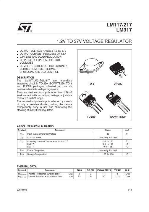
LM317_DataSheet
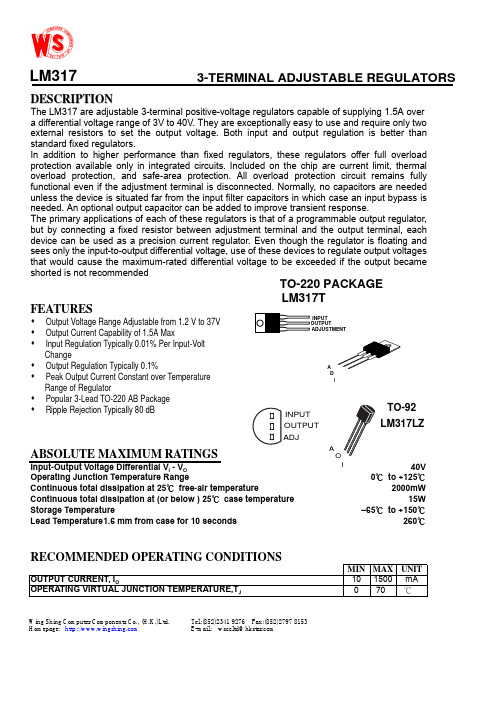
D E S C R I P T I O NThe LM 317 are adjustable 3-terminal positive-voltage regulators capable of supplying 1.5A over a differential voltage range of 3V to 40V. They are exceptionally easy to use and require only two external resistors to set the output voltage. Both input and output regulation is better than standard fixed regulators.In addition to higher performance than fixed regulators, these regulators offer full overload protection available only in integrated circuits. Included on the chip are current limit, thermal overload protection, and safe-area protection. All overload protection circuit remains fully functional even if the adjustment terminal is disconnected. Normally, no capacitors are needed unless the device is situated far from the input filter capacitors in which case an input bypass is needed. An optional output capacitor can be added to improve transient response.The primary applications of each of these regulators is that of a programmable output regulator,but by connecting a fixed resistor between adjustment terminal and the output terminal, each device can be used as a precision current regulator. Even though the regulator is floating and sees only the input-to-output differential voltage, use of these devices to regulate output voltages that would cause the maximum-rated differential voltage to be exceeded if the output became shorted is not recommendedFEATURES! Output Voltage Range Adjustable from 1.2 V to 37V ! Output Current Capability of 1.5A Max! Input Regulation Typically 0.01% Per Input-Volt Change! Output Regulation Typically 0.1%! Peak Output Current Constant over Temperature Range of Regulator! Popular 3-Lead TO-220 AB Package !Ripple Rejection Typically 80 dBABSOLUTE MAXIMUM RATINGSInput-Output Voltage Differential V I - V O 40VOperating Junction Temperature Range0℃ to +125℃Continuous total dissipation at 25℃ free-air temperature2000mWContinuous total dissipation at (or below ) 25℃ case temperature 15WStorage Temperature–65℃ to +150℃Lead Temperature1.6 mm from case for 10 seconds260℃RECOMMENDED OPERATING CONDITIONSMIN MAXUNITOUTPUT CURRENT, I O 101500mA OPERATING VIRTUAL JUNCTION TEMPERATURE,T J 070 ℃Wing Shing Computer Components Co., (H.K.)Ltd.Tel:(852)2341 9276Fax:(852)2797 8153Homepage:E-mail: wsccltd@3-TERMINAL ADJUSTABLE REGULATORSTO-220 PACKAGE INPUT ADJUSTMENTA D ILM317LM317TOITO-92LM317LZINPUT OUTPUT ADJELECTRICAL CHARACTERISTICSPARAMETERTEST CONDITIONSMIN TYP MAXUNITT J =MIN to MAX 0.010.04Input Regulation*2V I -V O =3V to 40V *3I O =10mA to 1.5A0.020.07%/V V O =10V , f=120HZ 65Ripple RejectionV O =10V , f=120HZ10-µF capacitor between ADJ and ground 6680dB V O ≤5V 525mV I O =10mA TO 1.5A,T J =25℃*3,V O >5V0.10.5%V O ≥5V2070mV Output RegulationI O =10mA to 1.5AV O >5V0.3 1.5%Output V oltage Change With Temperature T J =MIN to MAX1%Output V oltage long-term Drift*4After 1000h at T J = MAX and VI-VO=40V 0.31%Output Noise V oltagef=10Hz to 10kHz, T J =25℃0.003%Minimum Output Current to MaintainRegulationV I -V O =40V3.510mA V I -V O ≤15V1.52.2Peak Output CurrentV I -V O ≤40V , T J =250.150.4AAdjustment-terminal Current50100µA Change in adjustment-terminal CurrentV I -V O =2.5V to 40V ,I O =10mA to 1.5A0.25.0µA Reference V oltage(Output to ADJ) V I -V O=3V to 40V , IO=10mA to 1.5A,P ≤15W1.201.251.30V*1All characteristics are measured with a 0.1-µF capacitor across the input and a 1-µF capacitor across the output.*2Input regulation is expressed here as the percentage change in output voltage per 1-V change at the input*3Pulse testing techniques are used to maintain the junction temperature as close to the ambient temperature as possible.Thermal effects must be taken into account separately.*4Since long-term drift cannot be measured on the individual devices prior to shipment. This specification is not intended to be a guarantee or warranty. It is an engineering estimate of the average drift to be expected from lot to lot.TYPICAL APPLICATION DATA1. Use of an input bypass capacitor is recommended if regulator is far from filter capacitors.2. Use of an output capacitor improves transient response but is optional.3. V REF equals the difference between the output and adjustment terminal voltages.REGV I 0V O = V REF { 1+ }2R 13-TERMINAL ADJUSTABLE REGULATORSSee Note 3Uniess otherwise notedshown as MIN or MAX, use the appropriatevalue specified under recommended operating conditions.voltage is calculated fromPOSITIVE ADJUSTABLE REGULATORPAD LOCATION LM 317COORDINATESµm PAD N PAD NAME X Y 1ADJ 21204102OUTPUT 173014903INPUT 11209504OUTPUT901003-TERMINAL ADJUSTABLE REGULATORSLM317。
三端可调节输出正电压稳压器LM317T

三端可调节输出正电压稳压器LM317是可调节3端正电压稳压器,在输出电压范围为1.2伏到37伏时能够提供超过1.5安的电流。
此稳压器非常易于使用,只需要两个外部电阻来设置输出电压。
此外还使用内部限流、热关断和安全工作区补偿之基本能防止烧断保险丝。
LM317服务于多种应用场合,包括局部稳压、卡上稳压。
该器件还可以用来制伏一种可编程的输出稳压器,或者,通过在调整点和输出之间接一个固定电阻,LM317可用作一种精密稳流器。
*输出电流超过1.5A*输出在1.2~37V之间可调节*内部热过载保护*不随温度变化的内部短路电流限制*输出晶体管安全工作区补偿*对高压应用孚空工作*避免置备多种固定电压标准应用*专稳用器离电源港液器有…定距為时 6是必需的4Co对稔定性而言不必要;但改逬瞬态响応V CXJt= 1.25V( 1 + 务IgFG因为ly控制在小于10OuAiS •顶的淚差在多数应用中可忽路使W 317稳压器从零伏起调电路、LM317T应用电路一例(转载)lm317LM317作为输出电压可变的集成三端稳压块,是一种使用方便、应用广泛的集成稳压块。
317系列稳压块的型号很多:例如 LM317HVH 、W317L等。
电子爱好者经常用317稳压块制作输出电压可变的稳压电源。
稳压电源的输出电压可用下式计算,Vo = 1.25 ( 1 + R2/R1 )。
仅仅从公式本身看,R1、R2的电阻值可以随意设定。
然而作为稳压电源的输出电压计算公式,R1和R2的阻值是不能随意设定的。
首先317稳压块的输出电压变化范围是Vo = 1.25V — 37V (高输出电压的317稳压块如 LM317HVA、LM317HVK等,其输出电压变化范围是Vo = 1.25V — 45V ),所以 R2/R1的比值范围只能是0 — 28.6。
其次是317稳压块都有一个最小稳定工作电流,有的资料称为最小输出电流,也有的资料称为最小泄放电流。
最小稳定工作电流的值一般为 1.5mA。
- 1、下载文档前请自行甄别文档内容的完整性,平台不提供额外的编辑、内容补充、找答案等附加服务。
- 2、"仅部分预览"的文档,不可在线预览部分如存在完整性等问题,可反馈申请退款(可完整预览的文档不适用该条件!)。
- 3、如文档侵犯您的权益,请联系客服反馈,我们会尽快为您处理(人工客服工作时间:9:00-18:30)。
KA317 / LM317 — 3-Terminal Positive Adjustable Regulator3-Terminal Positive Adjustable RegulatorFeatures•Output-Current In Excess of 1.5 A•Output-Adjustable Between 1.2 V and 37 V •Internal Thermal Overload Protection •Internal Short-Circuit Current Limiting•Output-Transistor Safe Operating Area Compensation •TO-220 PackageOrdering InformationBlock DiagramProduct NumberPackagePacking MethodOperating TemperatureLM317T TO-220 (Single Gauge)Rail 0°C to +125°C KA317TUTO-220 (Dual Gauge)Rail0°C to +125°CRlimit3Vin Voltage ReferenceProtection CircuitryInputR LIMIT DescriptionThis monolithic integrated circuit is an adjustable 3-termi-nal positive-voltage regulator designed to supply more than 1.5 A of load current with an output voltage adjust-able over a 1.2 V to 37 V range. It employs internal cur-rent limiting, thermal shutdown, and safe area compensation.TO-2201. Adj2. Output3. Input1OutputKA317 / LM317 — 3-Terminal Positive Adjustable RegulatorAbsolute Maximum RatingsStresses exceeding the absolute maximum ratings may damage the device. The device may not function or be opera-ble above the recommended operating conditions and stressing the parts to these levels is not recommended. In addi-tion, extended exposure to stresses above the recommended operating conditions may affect device reliability. The absolute maximum ratings are stress ratings only. Values are at T A = 25°C unless otherwise noted.Thermal CharacteristicsSymbolParameterValueUnitV I - V O Input-Output Voltage Differential 40V T LEAD Lead Temperature230°C T J Operating Junction Temperature Range 0 to +125°C T STG Storage Temperature Range-65 to +125°C ΔV O /ΔTTemperature Coefficient of Output Voltage±0.02%/°CSymbolParameter ValueUnitsP D Power DissipationInternally LimitedW R θJA Thermal Resistance, Junction to Ambient 80°C/W R θJCThermal Resistance, Junction to Case5°C/WNotes:1. Load and line regulation are specified at constant junction temperature. Change in V D due to heating effects must be taken into account separately. Pulse testing with low duty is used (P MAX = 20 W).2. C ADJ , when used, is connected between the adjustment pin and ground.e N RMS Noise,% of V OUT T A = +25°C, 10 Hz ≤ f ≤ 10 kHz 0.0030.010%/V O RR Ripple RejectionV O = 10 V, f = 120 Hz without C ADJ 60dB C ADJ = 10 μF (2)6675dBSTLong-Term Stability, T J = T HIGH T A = +25°C for End Point Measurements, 1000 HR0.31.0%Figure 4. Dropout VoltageFigure 5. Reference VoltageFigure 6. Short Circuit vs Input-Output VoltageTEMPERATURE (°C)I N P U T -O U T P U T D TEMPERATURE (°C)R E F E R E N C 051015202530350123I S C - S H O R T C I R C U I T C U R R E N T (A )V I -V O - INPUT OUTPUT VOLTAGE [V]T A = 25oCV OUT = 1.25 V, Shorthed to GNDFigure 8. TO-220, MOLDED, 3-LEAD, JEDEC, VARIATION ABPackage drawings are provided as a service to customers considering Fairchild components. Drawings may change in any manner without notice. Please note the revision and/or date on the drawing and contact a Fairchild Semiconductor representative to verify or obtain the most recent revision. Package specifications do not expand the terms of Fairchild’s worldwide terms and conditions, specifically the warranty therein, which covers Fairchild products.Always visit Fairchild Semiconductor’s online packaging area for the most recent package drawings:Figure 9. TO220, MOLDED, 3-LEAD, NON-JEDEC, VARIATION ABPackage drawings are provided as a service to customers considering Fairchild components. Drawings may change in any manner without notice. Please note the revision and/or date on the drawing and contact a Fairchild Semiconductor representative to verify or obtain the most recent revision. Package specifications do not expand the terms of Fairchild’s worldwide terms and conditions, specifically the warranty therein, which covers Fairchild products.Always visit Fairchild Semiconductor’s online packaging area for the most recent package drawings:/dwg/TO/TO220Y03.pdf.TRADEMARKSThe following includes registered and unregistered trademarks and service marks, owned by Fairchild Semiconductor and/or its global subsidiaries, and is not intended to be an exhaustive list of all such trademarks. 2Cool ¥AccuPower ¥AX-CAP ®*BitSiC ¥Build it Now ¥CorePLUS ¥CorePOWER ¥CROSSVOLT ¥CTL ¥Current Transfer Logic ¥DEUXPEED ®Dual Cool™ EcoSPARK ®EfficientMax ¥ESBC ¥Fairchild ®Fairchild Semiconductor ®FACT Quiet Series ¥FACT ®FAST ®FastvCore ¥FETBench ¥FPS ¥F-PFS ¥FRFET ®Global Power Resource SMGreenBridge ¥Green FPS ¥Green FPS ¥ e-Series ¥G max ¥GTO ¥IntelliMAX ¥ISOPLANAR ¥Making Small Speakers Sound Louderand Better™MegaBuck ¥MICROCOUPLER ¥MicroFET ¥MicroPak ¥MicroPak2¥MillerDrive ¥MotionMax ¥mWSaver ¥OptoHiT ¥OPTOLOGIC ®OPTOPLANAR ®®PowerTrench ®PowerXS™Programmable Active Droop ¥QFET ®QS ¥Quiet Series ¥RapidConfigure ¥¥Saving our world, 1mW/W/kW at a time™ SignalWise ¥SmartMax ¥SMART START ¥Solutions for Your Success ¥SPM ®STEALTH ¥SuperFET ®SuperSOT ¥-3 SuperSOT ¥-6 SuperSOT ¥-8 SupreMOS ®SyncFET ¥Sync-Lock™®*TinyBoost ¥TinyBuck ¥TinyCalc ¥TinyLogic ®TINYOPTO ¥TinyPower ¥TinyPWM ¥TinyWire ¥TranSiC ¥TriFault Detect ¥TRUECURRENT ®*P SerDes ¥UHC ®Ultra FRFET ¥UniFET ¥VCX ¥VisualMax ¥VoltagePlus ¥XS™* Trademarks of System General Corporation, used under license by Fairchild Semiconductor.DISCLAIMERFAIRCHILD SEMICONDUCTOR RESERVES THE RIGHT TO MAKE CHANGES WITHOUT FURTHER NOTICE TO ANY PRODUCTS HEREIN TO IMPROVE RELIABILITY, FUNCTION, OR DESIGN. FAIRCHILD DOES NOT ASSUME ANY LIABILITY ARISING OUT OF THE APPLICATION OR USE OF ANY PRODUCT OR CIRCUIT DESCRIBED HEREIN; NEITHER DOES IT CONVEY ANY LICENSE UNDER ITS PATENT RIGHTS, NOR THE RIGHTS OF OTHERS. THESE SPECIFICATIONS DO NOT EXPAND THE TERMS OF FAIRCHILD’S WORLDWIDE TERMS AND CONDITIONS, SPECIFICALLY THE WARRANTY THEREIN, WHICH COVERS THESE PRODUCTS.LIFE SUPPORT POLICYFAIRCHILD’S PRODUCTS ARE NOT AUTHORIZED FOR USE AS CRITICAL COMPONENTS IN LIFE SUPPORT DEVICES OR SYSTEMS WITHOUT THE EXPRESS WRITTEN APPROVAL OF FAIRCHILD SEMICONDUCTOR CORPORATION. As used herein:1. Life support devices or systems are devices or systems which, (a) are intended for surgical implant into the body or (b) support or sustain life, and (c) whose failure to perform when properly used in accordance with instructions for use provided in the labeling, can be reasonably expected to result in a significant injury of the user.2. A critical component in any component of a life support, device, orsystem whose failure to perform can be reasonably expected to cause the failure of the life support device or system, or to affect its safety or effectiveness. ANTI-COUNTERFEITING POLICYFairchild Semiconductor Corporation's Anti-Counterfeiting Policy. Fairchild's Anti-Counterfeiting Policy is also stated on our external website, , under Sales Support.Counterfeiting of semiconductor parts is a growing problem in the industry. All manufacturers of semiconductor products are experiencing counterfeiting of their parts. Customers who inadvertently purchase counterfeit parts experience many problems such as loss of brand reputation, substandard performance, failed applications, and increased cost of production and manufacturing delays. Fairchild is taking strong measures to protect ourselves and our customers from the proliferation of counterfeit parts. Fairchild strongly encourages customers to purchase Fairchild parts either directly from Fairchild or from Authorized Fairchild Distributors who are listed by country on our web page cited above. Products customers buy either from Fairchild directly or from Authorized Fairchild Distributors are genuine parts, have full traceability, meet Fairchild's quality standards for handling and storage and provide access to Fairchild's full range of up-to-date technical and product information. Fairchild and our Authorized Distributors will stand behind all warranties and will appropriately address any warranty issues that may arise. Fairchild will not provide any warranty coverage or other assistance for parts bought from Unauthorized Sources. Fairchild is committed to combat this global problem and encourage our customers to do their part in stopping this practice by buying direct or from authorized distributors.PRODUCT STATUS DEFINITIONS Definition of TermsDatasheet IdentificationProduct StatusDefinitionAdvance Information Formative / In DesignDatasheet contains the design specifications for product development. Specifications may changein any manner without notice.P reliminary First ProductionDatasheet contains preliminary data; supplementary data will be published at a later date. FairchildSemiconductor reserves the right to make changes at any time without notice to improve design. No Identification Needed Full ProductionDatasheet contains final specifications. Fairchild Semiconductor reserves the right to makechanges at any time without notice to improve the design.Obsolete Not In ProductionDatasheet contains specifications on a product that is discontinued by Fairchild Semiconductor.The datasheet is for reference information only.Rev. I64®。
