FPGA可编程逻辑器件芯片XC6SLX16-2CS中文规格书
FPGA可编程逻辑器件芯片XC6VLX760-1FFG1760C中文规格书
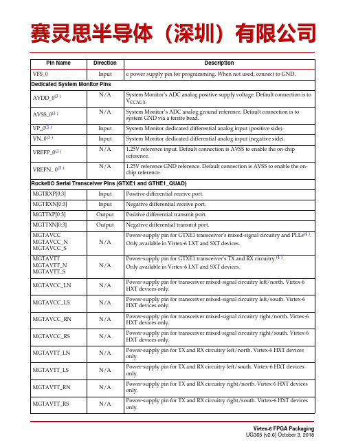
VFS_0Inpute power supply pin for programming. When not used, connect to GND.Dedicated System Monitor Pins AVDD_0(3)N/A System Monitor’s ADC analog positive supply voltage. Default connection is to V CCAUX .AVSS_0(3)N/A System Monitor’s ADC analog ground reference. Default connection is to system GND via a ferrite bead.VP_0(3)Input System Monitor dedicated differential analog input (positive side).VN_0(3)Input System Monitor dedicated differential analog input (negative side).VREFP_0(3)N/A 1.25V reference input. Default connection is AVSS to enable the on-chip reference.VREFN_ 0(3)N/A1.25V reference GND reference. Default connection is AVSS to enable the on-chip reference.RocketIO Serial Transceiver Pins (GTXE1 and GTHE1_QUAD)MGTRXP[0:3]Input Positive differential receive port.MGTRXN[0:3]Input Negative differential receive port.MGTTXP[0:3]Output Positive differential transmit port.MGTTXN[0:3]Output Negative differential transmit port.MGTAVCC MGTAVCC_N MGTAVCC_S N/APower-supply pin for GTXE1 transceiver’s mixed-signal circuitry and PLLs (4).Only available in Virtex-6 LXT and SXT devices.MGTAVTT MGTAVTT_N MGTAVTT_S N/APower-supply pin for GTXE1 transceiver’s TX and RX circuitry.(4).Only available in Virtex-6 LXT and SXT devices.MGTAVCC_LN N/A Power-supply pin for transceiver mixed-signal circuitry left/north. Virtex-6 HXT devices only.MGTAVCC_LS N/A Power-supply pin for transceiver mixed-signal circuitry left/south. Virtex-6 HXT devices only.MGTAVCC_RN N/A Power-supply pin for transceiver mixed-signal circuitry right/north. Virtex-6 HXT devices only.MGTAVCC_RS N/A Power-supply pin for transceiver mixed-signal circuitry right/south. Virtex-6 HXT devices only.MGTAVTT_LN N/A Power-supply pin for TX and RX circuitry left/north. Virtex-6 HXT devices only.MGTAVTT_LS N/A Power-supply pin for TX and RX circuitry left/south. Virtex-6 HXT devices only.MGTAVTT_RN N/A Power-supply pin for TX and RX circuitry right/north. Virtex-6 HXT devices only.MGTAVTT_RSN/APower-supply pin for TX and RX circuitry right/south. Virtex-6 HXT devices only.Pin Name Direction DescriptionTable 2-2:FF784/RF784 Package—LX75T, LX130T, LX195T, and LX240T (Cont’d) Bank Pin Description Pin Number NoConnect (NC) 25IO_L18P_GC_25H2025IO_L18N_GC_25G2125IO_L19P_GC_25F2025IO_L19N_GC_25F2126IO_L0P_26E1226IO_L0N_26D1126IO_L1P_26E1326IO_L1N_26E1426IO_L2P_26H1626IO_L2N_26G1626IO_L3P_26G1426IO_L3N_26F1426IO_L4P_26J1626IO_L4N_VREF_26H1526IO_L5P_26B1126IO_L5N_26C1126IO_L6P_26D1326IO_L6N_26D1226IO_L7P_26C1426IO_L7N_26B1326IO_L8P_SRCC_26J1526IO_L8N_SRCC_26K1526IO_L9P_MRCC_26B1426IO_L9N_MRCC_26A1426IO_L10P_MRCC_26F1626IO_L10N_MRCC_26F1526IO_L11P_SRCC_26G1226IO_L11N_SRCC_26F1226IO_L12P_VRN_26E1526IO_L12N_VRP_26D1526IO_L13P_26A1526IO_L13N_26A1626IO_L14P_26A11FF1156/RF1156 Package—LX130T, LX195T, LX240T, LX365T, SX315T, and SX475T Table 2-5:FF1156/RF1156 Package—LX130T, LX195T, LX240T, LX365T, SX315T, and SX475T (Cont’d)Bank Pin Description Pin Number No Connect (NC) 25IO_L18P_GC_25H2825IO_L18N_GC_25H2925IO_L19P_GC_25B3125IO_L19N_GC_25A3126IO_L0P_26C2026IO_L0N_26D2026IO_L1P_26A2326IO_L1N_26A2426IO_L2P_26G2126IO_L2N_26G2226IO_L3P_26B2326IO_L3N_26C2326IO_L4P_26J2026IO_L4N_VREF_26J2126IO_L5P_26B2126IO_L5N_26B2226IO_L6P_26E2226IO_L6N_26E2326IO_L7P_26A2026IO_L7N_26A2126IO_L8P_SRCC_26F1926IO_L8N_SRCC_26F2026IO_L9P_MRCC_26B2026IO_L9N_MRCC_26C1926IO_L10P_MRCC_26F2126IO_L10N_MRCC_26G2026IO_L11P_SRCC_26H1926IO_L11N_SRCC_26H2026IO_L12P_VRN_26D2126IO_L12N_VRP_26E2126IO_L13P_26E1926IO_L13N_26D19Chapter 2:Pinout TablesTable 2-5:FF1156/RF1156 Package—LX130T, LX195T, LX240T, LX365T, SX315T,and SX475T (Cont’d)Bank Pin Description Pin Number No Connect (NC)26IO_L14P_26H2226IO_L14N_VREF_26J2226IO_L15P_26A1826IO_L15N_26A1926IO_L16P_26K2126IO_L16N_26K2226IO_L17P_26B1826IO_L17N_26C1826IO_L18P_26L2026IO_L18N_26L2126IO_L19P_26C2226IO_L19N_26D2232IO_L0P_32AG1532IO_L0N_32AF1532IO_L1P_32AK1432IO_L1N_32AJ1432IO_L2P_32AJ1532IO_L2N_32AH1532IO_L3P_32AL1532IO_L3N_32AL1432IO_L4P_32AG1632IO_L4N_VREF_32AF1632IO_L5P_32AN1532IO_L5N_32AM1532IO_L6P_32AJ1732IO_L6N_32AJ1632IO_L7P_32AP1632IO_L7N_32AP1532IO_L8P_SRCC_32AH1732IO_L8N_SRCC_32AG1732IO_L9P_MRCC_32AC1532IO_L9N_MRCC_32AD15。
FPGA可编程逻辑器件芯片5CGXFC7C6F23I7N中文规格书
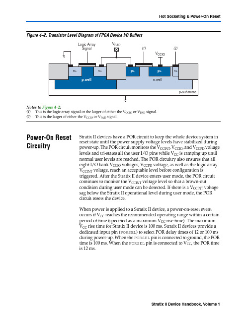
Hot Socketing & Power-On Reset Figure4–2.Transistor Level Diagram of FPGA Device I/O BuffersNotes to Figure4–2:(1)This is the logic array signal or the larger of either the V CCIO or V PAD signal.(2)This is the larger of either the V CCIO or V PAD signal.Power-On Reset Circuitry Stratix II devices have a POR circuit to keep the whole device system in reset state until the power supply voltage levels have stabilized during power-up. The POR circuit monitors the V CCINT, V CCIO, and V CCPD voltage levels and tri-states all the user I/O pins while V CC is ramping up until normal user levels are reached. The POR circuitry also ensures that all eight I/O bank V CCIO voltages, V CCPD voltage, as well as the logic array V CCINT voltage, reach an acceptable level before configuration is triggered. After the Stratix II device enters user mode, the POR circuit continues to monitor the V CCINT voltage level so that a brown-out condition during user mode can be detected. If there is a V CCINT voltage sag below the Stratix II operational level during user mode, the POR circuit resets the device.When power is applied to a Stratix II device, a power-on-reset event occurs if V CC reaches the recommended operating range within a certain period of time (specified as a maximum V CC rise time). The maximum V CC rise time for Stratix II device is 100 ms. Stratix II devices provide a dedicated input pin (PORSEL) to select POR delay times of 12 or 100 ms during power-up. When the PORSEL pin is connected to ground, the POR time is 100 ms. When the PORSEL pin is connected to V CC, the POR time is 12 ms.TriMatrix Embedded Memory Blocks in Stratix II and Stratix II GX Devices Figure2–8.Stratix II and Stratix II GX Simple Dual-Port Timing WaveformsNotes to Figure2–8:(1)The crosses in the data waveform during read mean “don’t care.”(2)The read enable rden signal is not available in M-RAM blocks. The M-RAM block in simple dual-port mode alwaysreads out the data stored at the current read address location.True Dual-Port ModeStratix II and Stratix II GX M4K and M-RAM memory blocks support thetrue dual-port mode. True dual-port mode supports any combination oftwo-port operations: two reads, two writes, or one read and one write attwo different clock frequencies. Figure2–9 shows Stratix II andStratix II GX true dual-port memory configuration.Figure2–9.Stratix II and Stratix II GX True Dual-Port Memory Note(1)Note to Figure2–9:(1)True dual-port memory supports input/output clock mode in addition to theindependent clock mode shown.TriMatrix MemoryTriMatrixMemory TriMatrix memory consists of three types of RAM blocks: M512, M4K, and M-RAM. Although these memory blocks are different, they can allimplement various types of memory with or without parity, including true dual-port, simple dual-port, and single-port RAM, ROM, and FIFO buffers. Table 2–3 shows the size and features of the different RAM blocks.Column IOEv v v Row IOE v v v vTable 2–2. Stratix II Device Routing Scheme (Part 2 of 2)Source DestinationS h a r e d A r i t h m e t i c C h a i nC a r r y C h a i n R e g i s t e r C h a i n L o c a l I n t e r c o n n e c tD i r e c t L i n k I n t e r c o n n e c t R 4 I n t e r c o n n e c t R 24 I n t e r c o n n e c t C 4 I n t e r c o n n e c t C 16 I n t e r c o n n e c t A L M M 512 R A M B l o c k M 4K R A M B l o c k M -R A M B l o c k D S P B l o c k sC o l u m n I O E R o w I O E Table 2–3.TriMatrix Memory Features (Part 1 of 2)Memory FeatureM512 RAM Block (32×18 Bits)M4K RAM Block (128×36 Bits)M-RAM Block (4K ×144Bits)Maximum performance500 MHz 550 MHz 420 MHz T rue dual-port memoryv v Simple dual-port memoryv v v Single-port memoryv v v Shift registerv v ROMv v (1)FIFO bufferv v v Pack modev v Byte enablev v v Address clock enablev v Parity bitsv v v Mixed clock modev v v Memory initialization (.mif )v v。
FPGA可编程逻辑器件芯片XC6SLX75-2CSG484I中文规格书
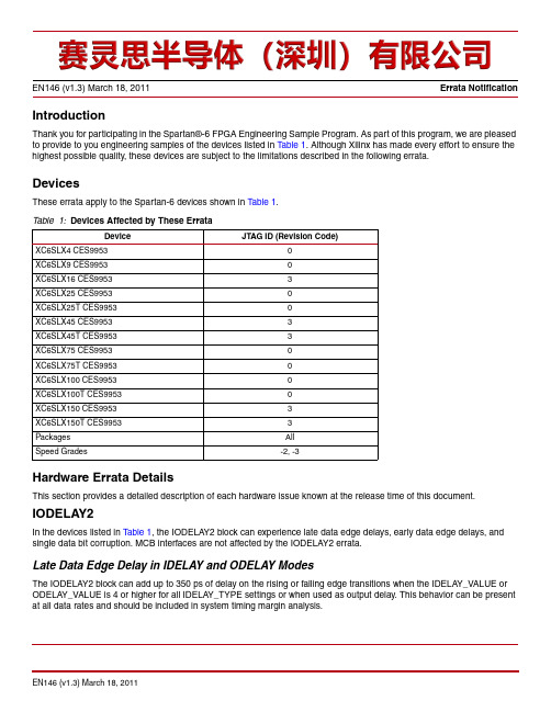
IntroductionThank you for participating in the Spartan®-6 FPGA Engineering Sample Program. As part of this program, we are pleased to provide to you engineering samples of the devices listed in T able 1. Although Xilinx has made every effort to ensure the highest possible quality, these devices are subject to the limitations described in the following errata.DevicesThese errata apply to the Spartan-6 devices shown in Table 1.Hardware Errata DetailsThis section provides a detailed description of each hardware issue known at the release time of this document.IODELAY2In the devices listed in Table 1, the IODELAY2 block can experience late data edge delays, early data edge delays, and single data bit corruption. MCB interfaces are not affected by the IODELAY2 errata.Late Data Edge Delay in IDELAY and ODELAY ModesThe IODELAY2 block can add up to 350ps of delay on the rising or falling edge transitions when the IDELAY_VALUE or ODELAY_VALUE is 4 or higher for all IDELAY_TYPE settings or when used as output delay. This behavior can be present at all data rates and should be included in system timing margin analysis.EN146 (v1.3) March 18, 2011Errata NotificationTable 1:Devices Affected by These ErrataDeviceJTAG ID (Revision Code)XC6SLX4 CES99530XC6SLX9 CES99530XC6SLX16 CES99533XC6SLX25 CES99530XC6SLX25T CES99530XC6SLX45 CES99533XC6SLX45T CES99533XC6SLX75 CES99530XC6SLX75T CES99530XC6SLX100 CES99530XC6SLX100T CES99530XC6SLX150 CES99533XC6SLX150T CES99533Packages All Speed Grades-2, -3Block RAMDual Port Block RAM Address Overlap in READ_FIRST and Simple Dual Port ModeWhen using the block RAM in True Dual Port (TDP) READ_FIRST mode or Simple Dual Port (SDP) mode, with different clocks on ports A and B, the user must ensure certain addresses do not occur simultaneously on both ports when both ports are enabled and one port is being written to. Failure to observe this restriction can result in read and/or memory array corruption.The description is found in the Conflict Avoidance section in v1.2 of UG383, the Spartan-6 FPGA Block RAM Resources User Guide.This description was originally added to the Spartan-6 FPGA Block RAM Resources User Guide, v1.1, published 10/28/09. This errata is being provided to highlight this change and ensure that all users are aware of this design restriction. ISE® 12.1 software provides appropriate warnings for possible violations of these restrictions.This issue will not be fixed in the devices listed in Table1.Work-aroundThe recommended work-around to avoid memory array corruption issue is to configure the block RAM inWRITE_FIRST mode. WRITE_FIRST mode is available in block RAMs configured in TDP mode in all ISE software versions. WRITE_FIRST mode is available in block RAMs configured in SDP mode from ISE v12.3 and later.See Answer Record 34533.performance mode when operating within the standard V CCINT recommended operating conditions. In addition, a new Extended MCB performance mode has been introduced with V CCINT operating conditions that allow the MCB to operate at the originally specified performance.Table 3:MCB Performance Specification ComparisonPerformance Specification V CCINT Operating RangeDDR2 / DDR3 Performance-2-3Original (No Longer Supported) 1.14V – 1.26V667Mb/s800Mb/s New (Standard Performance) 1.14V – 1.26V625Mb/s667Mb/s New (Extended Performance) 1.2V – 1.26V667Mb/s800Mb/sSCD9953 Test ConditionsThe devices listed in Table1 support the Industrial temperature range (T j=–40°C to +100°C), unless otherwise specified.Operational GuidelinesDesign Software RequirementsThe devices listed in Table1, unless otherwise specified, require the following Xilinx development software installation:•Speed specification v1.08 (or later), Xilinx ISE Design Suite 12.1 (or later).TraceabilityThe XC6SLX45T is marked as shown in Figure1. The other devices in Table1 are marked similarly.Revision History Figure 1:Example Device Top Mark质量等级领域:宇航级IC、特军级IC、超军级IC、普军级IC、禁运IC、工业级IC,军级二三极管,功率管等;应用领域:航空航天、船舶、汽车电子、军用计算机、铁路、医疗电子、通信网络、电力工业以及大型工业设备祝您:工作顺利,生活愉快!以赛灵思半导体(深圳)有限公司提供的参数为例,以下为XC6SLX75-2CSG484I的详细参数,仅供参考。
FPGA可编程逻辑器件芯片XC2S100-6CS144C中文规格书

FPGA可编程逻辑器件芯⽚XC2S100-6CS144C中⽂规格书Configuration Sequence supply sequencing requirements. Power V CCO last after V CCINT and V CCAUX to ensurethat the outputs stay disabled until configuration begins.All JTAG and serial configuration pins are located in V CCAUX and VCCO_2 supply banks. The dual-purpose pins are located in Banks 0, 1, and 2 (one exception is A24 and A25 are in bank5 for larger devices with 6 I/O banks). The DONE and PROGRAM_B dedicated inputs operate at the VCCO_2 LVCMOS level, and the JTAG input pins (TCK, TMS, and TDI) and the SUSPEND pin operate at the V CCAUX LVCMOS level. The DONE pin operates at the VCCO_2 voltage level with the output standard set to LVCMOS 8mA SLOW. TDO drives at the voltage level provided on V CCAUX at 8 mA SLOW.For all modes that use dual-purpose I/O, the associated VCCO_X must be connected to the appropriate voltage to match the I/O standard of the configuration device. HSWAPEN requires that VCCO_0 be supplied, and DOUT requires that VCCO_1 be supplied. The pins are also LVCMOS18, LVCMOS25, or LVCMOS33 8mA SLOW during configuration, depending on the VCCO_X level.For power-up, the V CCINT power pins must be supplied with 1.2V for -2/-3 speed grades and 1.0V for -1L sources. VCCO_2 must be supplied. Table5-11 shows the power supplies required for configuration. Table5-12 shows the timing for power-up. Table 5-11:Power Supplies Required for ConfigurationPin Name(1)DescriptionV CCINT Internal core voltage.V BATT(2)Encryption Key battery supply. If there is no encryption keybeing stored in the volatile memory, V BATT should beconnected to V CCAUX or GND, or left unconnected.V FS Encryption Key eFUSE programming voltage. If eFUSEprogramming is not needed, connect V FS to V CC or GND(recommended).V CCAUX(3)Auxiliary power input for configuration logic and other FPGAfunctions.VCCO_0 VCCO_1 VCCO_2(4) VCCO_5(5)Dual-purpose configuration pin output supply voltage. VCCO_2 cannot be 1.2V or 1.5V during configuration.Notes:1.For recommended operating values, refer to DS162, Spartan-6 FPGA Data Sheet: DC and Switching Characteristics.2.V BATT or V FS are required only when using bitstream encryption and are only supported in Spartan-6LX75, LX75T, LX100, LX100T, LX150, and LX150T devices.3.V CCAUX must be greater than or equal to V FS during eFUSE programming. This requirement is notnecessary for configuration.4.If VCCO_2 is 1.8V, V CCAUX must be 2.5V. If VCCO_2 is 2.5V or 3.3V, V CCAUX can be either 2.5V or 3.3V.5.VCCO_5 might be needed if BPI configuration mode is used and A24 and A25 are in I/O Bank 5.Chapter 5:Configuration DetailsConfiguration Options Register (COR1 and COR2)The Configuration Options Register is used to set certain configuration options for the device. The name of each bit position in COR1 and COR2 is given in Table5-36. Table 5-36:Configuration Options (COR1 and COR2) DescriptionsRegister Field Bit Index Description BitGen DefaultCOR1DRIVE_AWAKE150: Does not drive the awake pin (open drain).1: Actively drives the awake pin.RESERVED14:5Reserved.0110111000CRC_BYPASS4Does not check against the updated CRC value.0DONE_PIPE30: No pipeline stage for DONEIN.1: Add pipeline stage to DONEIN.DRIVE_DONE20: DONE pin is open drain.1: DONE pin is actively driven High.SSCLKSRC1:0Startup sequence clock.00: CCLK.01: UserClk.1x: TCK.00COR2RESET_ON_ERROR15Option to fallback when a crc_error occurs.0: Disable reset on error.1: Enable reset on error.0 RESERVED14:12Reserved000DONE_CYCLE11:9Startup phase in which DONE pin is released.(001,010,011,100,101,110)100LCK_CYCLE8:6Stall in this startup phase until DCM or PLL lock isasserted. (001,010,011,100,101,110,111wait>)111 (No wait)GTS_CYCLE5:3Startup phase in which I/Os switch from 3-state to userdesign.(000, 001,010,011,100,101,110,111)101GWE_CYCLE2:0Startup phase in which the global write enable is asserted.(000, 001,010,011,100,101,110,111)110Configuration PacketsSuspend Register (PWRDN_REG)Frame Length RegisterFrame Length Register (FLR) is written with the length of a frame, as measured in 16-bit words, near the beginning of the configuration bitstream. FLR must be written before any FDR operation will work. It is not necessary to set the FLR more than once.The actual value written to FLR = Actual Frame Length.Based on the segmentation scheme in Spartan-6 devices, the frame length for type0 (CLB, IOI, and special blocks) and type1 (block RAM) are fixed. The only block that needs a specified frame length is IOB.Multi-Frame Write RegisterThe Spartan-6 FPGA supports Multi-Frame Write (MFWR) for first-time configuration but does not support it during reconfiguration. The FPGA has to go through one power cycle or use PROGRAM_B to reset the chip before MFWR can be used.Table 5-37:Power-Down Register Description Field Bit IndexDescriptionBitGen DefaultRESERVED 15Reserved.EN_EYES14Enable Multi-Pin Wake-Up.0: Disable Multi-Pin Wake-Up.1: Enable Multi-Pin Wake-Up.0RESERVED 13:6Reserved.0010_0010FILTER_B 50: Suspend filter (300ns) on.1: Filter off.0EN_PGSR40: No GSR pulse during return from Suspend.1: Generate GSR pulse during return from Suspend.0RESERVED 3Reserved.EN_PWRDN 20: Suspend is disabled.1: Suspend is enabled.0KEEP_SCLK0: Use MCCLK for startup sequence initiated by power-up.1: Use SSCLKSRC for startup sequence initiated by power-up.1Table 5-38:Frame Length RegisterBits FLR[15:0]xxxxxxxxxxxxxxxxChapter 5:Configuration DetailsConfiguration Packets。
FPGA可编程逻辑器件芯片XC2S600E-6FGG456C中文规格书

Spartan-3 FPGA Design DocumentationThe functionality of the Spartan®-3 FPGA family is described in the following documents. The topics covered in each guide are listed.•UG331: Spartan-3 Generation FPGA User Guide •Clocking Resources•Digital Clock Managers (DCMs)•Block RAM•Configurable Logic Blocks (CLBs)-Distributed RAM -SRL16 Shift Registers -Carry and Arithmetic Logic•I/O Resources•Embedded Multiplier Blocks •Programmable Interconnect •ISE® Software Design Tools •IP C ores•Embedded Processing and Control Solutions •Pin Types and Package Overview •Package Drawings •Powering FPGAs•UG332: Spartan-3 Generation Configuration User Guide •Configuration Overview -Configuration Pins and Behavior -Bitstream Sizes•Detailed Descriptions by Mode-Master Serial Mode using Xilinx Platform Flash PROM-Slave Parallel (SelectMAP) using a Processor -Slave Serial using a Processor -JTAG Mode•ISE iMPACT Programming ExamplesCreate a Xilinx user account and sign up to receiveautomatic e-mail notification whenever this data sheet or the associated user guides are updated.For specific hardware examples, see the Spartan-3 FPGA Starter Kit board web page, which has links to various design examples and the user guide.DS099 (v3.1) June 27, 2013Product SpecificationThe output frequency (f CLKFX) can be expressed as a function of the incoming clock frequency (f CLKIN) as follows:f CLKFX = f CLKIN(CLKFX_MULTIPL Y/CLKFX_DIVIDE)Equation3 Regarding the two attributes, it is possible to assign any combination of integer values, provided that two conditions are met:•The two values fall within their corresponding ranges, as specified in Table18.•The f CLKFX frequency calculated from the above expression accords with the DCM’s operating frequency specifications.For example, if CLKFX_MULTIPL Y = 5 and CLKFX_DIVIDE = 3, then the frequency of the output clock signal would be 5/3 that of the input clock signal.DFS Frequency ModesThe DFS supports two operating modes, High Frequency and Low Frequency, with each specified over a different clock frequency range. The DFS_FREQUENCY_MODE attribute chooses between the two modes. When the attribute is set to LOW, the Low Frequency mode permits the two DFS outputs to operate over a low-to-moderate frequency range. When the attribute is set to HIGH, the High Frequency mode allows both these outputs to operate at the highest possible frequencies. DFS With or Without the DLLThe DFS component can be used with or without the DLL component:Without the DLL, the DFS component multiplies or divides the CLKIN signal frequency according to the respective CLKFX_MULTIPL Y and CLKFX_DIVIDE values, generating a clock with the new target frequency on the CLKFX and CLKFX180 outputs. Though classified as belonging to the DLL component, the CLKIN input is shared with the DFS component. This case does not employ feedback loop; therefore, it cannot correct for clock distribution delay.With the DLL, the DFS operates as described in the preceding case, only with the additional benefit of eliminating the clock distribution delay. In this case, a feedback loop from the CLK0 output to the CLKFB input must be present.The DLL and DFS components work together to achieve this phase correction as follows: Given values for theCLKFX_MULTIPL Y and CLKFX_DIVIDE attributes, the DLL selects the delay element for which the output clock edge coincides with the input clock edge whenever mathematically possible. For example, when CLKFX_MULTIPL Y = 5 and CLKFX_DIVIDE = 3, the input and output clock edges will coincide every three input periods, which is equivalent in time to five output periods.Smaller CLKFX_MULTIPL Y and CLKFX_DIVIDE values achieve faster lock times. With no factors common to the two attributes, alignment will occur once with every number of cycles equal to the CLKFX_DIVIDE value. Therefore, it is recommended that the user reduce these values by factoring wherever possible. For example, given CLKFX_MULTIPL Y = 9 and CLKFX_DIVIDE = 6, removing a factor of three yields CLKFX_MULTIPL Y = 3 and CLKFX_DIVIDE = 2. While both value-pairs will result in the multiplication of clock frequency by 3/2, the latter value-pair will enable the DLL to lock more quickly.Table 18:DFS AttributesAttribute Description ValuesDFS_FREQUENCY_MODE Chooses between High Frequency and Low Frequency modes Low, HighCLKFX_MULTIPL Y Frequency multiplier constant Integer from 2 to 32 CLKFX_DIVIDE Frequency divisor constant Integer from 1 to 32Table 19:DFS SignalsSignal Direction DescriptionCLKFX Output Multiplies the CLKIN frequency by the attribute-value ratio (CLKFX_MULTIPL Y/CLKFX_DIVIDE) to generate a clock signal with a new target frequency.CLKFX180Output Generates a clock signal with same frequency as CLKFX, only shifted 180° out-of-phase.Both the Fixed Phase and Variable Phase operating modes employ this calculation. If the PHASE_SHIFT value is zero, then CLKFB and CLKIN will be in phase, the same as when the PS component is disabled. When the PHASE_SHIFT value is positive, the CLKFB signal will be shifted later in time with respect to CLKIN. If the attribute value is negative, the CLKFB signal will be shifted earlier in time with respect to CLKIN.The Fixed Phase ModeThis mode fixes the desired fine phase shift to a fraction of the T CLKIN, as determined by Equation4 and its user-selected PHASE_SHIFT value P. The set of waveforms insection [b] of Figure22 illustrates the relationship between CLKFB and CLKIN in the Fixed Phase mode. In the Fixed Phase mode, the PSEN, PSCLK and PSINCDEC inputs are not used andmust be tied to GND. Fixed phase shift requires ISE software version 10.1.03 or later.ConfigurationSpartan-3 devices are configured by loading application specific configuration data into the internal configuration memory. Configuration is carried out using a subset of the device pins, some of which are "Dedicated" to one function only, while others, indicated by the term "Dual-Purpose", can be re-used as general-purpose User I/Os once configuration is complete.Depending on the system design, several configuration modes are supported, selectable via mode pins. The mode pins M0, M1, and M2 are Dedicated pins. The mode pin settings are shown in Table 26.The HSWAP_EN input pin defines whether the I/O pins that are not actively used during configuration have pull-up resistorsduring configuration. By default, HSWAP_EN is tied High (via an internal pull-up resistor if left floating) which shuts off the pull-up resistors on the user I/O pins during configuration. When HSWAP_EN is tied Low, user I/Os have pull-ups during configuration. The Dedicated configuration pins (CCLK, DONE, PROG_B, M2, M1, M0, HSWAP_EN) and the JTAG pins (TDI, TMS, TCK, and TDO) always have a pull-up resistor to VCCAUX during configuration, regardless of the value on the HSWAP_EN pin. Similarly, the dual-purpose INIT_B pin has an internal pull-up resistor to VCCO_4 or VCCO_BOTTOM, depending on the package style.Depending on the chosen configuration mode, the FPGA either generates a CCLK output, or CCLK is an input accepting an externally generated clock.A persist option is available which can be used to force the configuration pins to retain their configuration function even after device configuration is complete. If the persist option is not selected then the configuration pins with the exception of CCLK, PROG_B, and DONE can be used as user I/O in normal operation. The persist option does not apply to the boundary-scan related pins. The persist feature is valuable in applications that readback configuration data after entering the User mode.Table 27 lists the total number of bits required to configure each FPGA as well as the PROMs suitable for storing those bits. See DS123: Platform Flash In-System Programmable Configuration PROMs data sheet for more information.The maximum bitstream length that Spartan-3 FPGAs support in serial daisy-chains is 4,294,967,264 bits (4Gbits), roughly equivalent to a daisy-chain with 323 XC3S5000 FPGAs. This is a limit only for serial daisy-chains where configuration data is passed via the FPGA’s DOUT pin. There is no such limit for JTAG chains.Table 26:Spartan-3 FPGAs Configuration Mode Pin SettingsConfiguration Mode (1)M0M1M2Synchronizing ClockData WidthSerial DOUT (2)Master Serial 000CCLK Output 1Y es Slave Serial 111CCLK Input 1Y es Master Parallel 110CCLK Output 8No Slave Parallel 011CCLK Input 8No JTAG 11TC K Input1NoNotes:1.The voltage levels on the M0, M1, and M2 pins select the configuration mode.2.The daisy chain is possible only in the Serial modes when DOUT is used.Table 27:Spartan-3 FPGA Configuration DataDevice File Sizes Xilinx Platform Flash PROMSerial ConfigurationParallel ConfigurationXC3S50439,264XCF01S XCF08P XC3S2001,047,616XCF01S XCF08P XC3S4001,699,136XCF02S XCF08P XC3S10003,223,488XCF04S XCF08P XC3S15005,214,784XCF08P XCF08P XC3S20007,673,024XCF08P XCF08P XC3S400011,316,864XCF16P XCF16P XC3S500013,271,936XCF16PXCF16P。
FPGA可编程逻辑器件芯片EP3C16U256C6N中文规格书

920
966
1657 1739 1904 2013 ps
892
936
1585 1663 1821 1916 ps
912
958
1651 1733 1897 2006 ps
877
919
1385 1453 1591 1680 ps
897
941
1451 1523 1667 1770 ps
879
921
1394 1462 1602 1691 ps
VSWING AC differential input voltage (AC)
VISO
Input clock signal offset
voltage
ΔVISO
Input clock signal offset voltage variation
VOX (AC)
AC differential cross point voltage
Stratix II Device Handbook, Volume 1
DC & Switching Characteristics
Table 5–17. SSTL-18 Class II Specifications
Symbol
Parameter
Conditions
Minimum
Typical Maximum Unit
Figure 4–2 shows a transistor level cross section of the Stratix II device I/O buffers. This design ensures that the output buffers do not drive when VCCIO is powered before VCCINT or if the I/O pad voltage is higher than VCCIO. This also applies for sudden voltage spikes during hot insertion. There is no current path from signal I/O pins to VCCINT or VCCIO or VCCPD during hot insertion. The VPAD leakage current charges the 3.3-V tolerant circuit capacitance.
FPGA可编程逻辑器件芯片XC6SLX9-2CSG225I中文规格书

Spartan-6 FPGA Electrical CharacteristicsSpartan®-6 LX and LXT FPGAs are available in various speed grades, with -3 having the highest performance. The DC and AC electrical parameters of the Automotive XA Spartan-6 FPGAs and Defense-grade Spartan-6Q FPGAs devices are equivalent to the commercial specifications except where noted. The timing characteristics of the commercial (XC) -2 speed grade industrial device are the same as for a -2 speed grade commercial device. The -2Q and -3Q speed grades areexclusively for the expanded (Q) temperature range. The timing characteristics are equivalent to those shown for the -2 and -3 speed grades for the Automotive and Defense-grade devices.Spartan-6FPGA DC and AC characteristics are specified for commercial (C), industrial (I), and expanded (Q) temperature ranges. Only selected speed grades and/or devices might be available in the industrial or expanded temperature ranges for Automotive and Defense-grade devices. References to device names refer to all available variations of that part number (for example, LX75 could denote XC6SLX75, XA6SLX75, or XQ6SLX75). The Spartan-6 FPGA -3N speed grade designates devices that do not support MCB functionality.All supply voltage and junction temperature specifications are representative of worst-case conditions. The parameters included are common to popular designs and typical applications. Available device and package combinations can be found at:•DS160: Spartan-6 Family Overview•DS170: Automotive XA Spartan-6 Family Overview •DS172: Defense-Grade Spartan-6Q Family OverviewSpartan-6 FPGA DC CharacteristicsSpartan-6 FPGA Data Sheet:DC and Switching CharacteristicsDS162 (v3.1.1) January 30, 2015Product SpecificationTable 1:Absolute Maximum Ratings (1)Symbol DescriptionUnits V CCINT Internal supply voltage relative to GND –0.5 to 1.32V V CCAUX Auxiliary supply voltage relative to GND –0.5 to 3.75V V CCO Output drivers supply voltage relative to GND–0.5 to 3.75V V BATT Key memory battery backup supply (LX75, LX75T, LX100, LX100T , LX150, and LX150T only)–0.5 to 4.05V V FS External voltage supply for eFUSE programming (LX75, LX75T , LX100, LX100T, LX150, and LX150T only)(2)–0.5 to 3.75V V REFInput reference voltage–0.5 to 3.75VeFUSE Read EnduranceTable11 lists the minimum guaranteed number of read cycle operations for Device DNA and for the AES eFUSE key. For more information, see UG380: Spartan-6 FPGA Configuration User Guide.Table 11:eFUSE Read EnduranceSymbol DescriptionSpeed Grade Units(Min) -3-3N-2-1LDNA_CYCLES Number of DNA_PORT READ operations or JT AG ISC_DNA read command operations. Unaffected by SHIFT operations.30,000,000ReadCyclesAES_CYCLES Number of JTAG FUSE_KEY or FUSE_CNTL read command operations.Unaffected by SHIFT operations.30,000,000ReadCyclesSSTL, Class II, 2.5V SSTL2_II 250V REF 1.25SSTL, Class II, 1.5VSSTL15_II250V REF 0.75LVDS (Low-Voltage Differential Signaling), 2.5V & 3.3V LVDS_25, LVDS_3310000(3)–BLVDS (Bus LVDS), 2.5V BLVDS_25Note 400(3)–Mini-LVDS, 2.5V & 3.3VMINI_LVDS_25, MINI_LVDS_3310000(3)–RSDS (Reduced Swing Differential Signaling), 2.5V & 3.3V RSDS_25, RSDS_3310000(3)–TMDS (Transition Minimized Differential Signaling), 3.3V TMDS_33Note 500(3)–PPDS (Point-to-Point Differential Signaling, 2.5V & 3.3VPPDS_25, PPDS_331000(3)–DescriptionI/O Standard Attribute R REF (Ω)C REF (1)(pF)V MEAS (V)V REF (V)Table 33:Spartan-6 FPGA V CCO/GND Pairs per BankPackage Devices Description Bank 0Bank 1Bank 2Bank 3Bank 4Bank 5TQG144LX V CCO/GND Pairs3323N/A N/A Maximum I/O per Pair88138N/A N/ACPG196LX VCCO/GND Pairs4646N/A N/A Maximum I/O per Pair6474N/A N/ACSG225LX V CCO/GND Pairs4444N/A N/A Maximum I/O per Pair1010910N/A N/AFT(G)256LX V CCO/GND Pairs5645N/A N/A Maximum I/O per Pair89910N/A N/ACSG324LXV CCO/GND Pairs6666N/A N/AMaximum I/O per Pair109109N/A N/A LXTV CCO/GND Pairs4666N/A N/AMaximum I/O per Pair49109N/A N/ACS(G)484LXV CCO/GND Pairs813813N/A N/AMaximum I/O per Pair7878N/A N/A LXTV CCO/GND Pairs712813N/A N/AMaximum I/O per Pair5868N/A N/AFG(G)484LXV CCO/GND Pairs10101111N/A N/AMaximum I/O per Pair6898N/A N/A LXTV CCO/GND Pairs6101110N/A N/AMaximum I/O per Pair7878N/A N/AFG(G)676LX45V CCO/GND Pairs12151016N/A N/AMaximum I/O per Pair3787N/A N/A LX75, LX100, LX150V CCO/GND Pairs129101066Maximum I/O per Pair9109989 LXTV CCO/GND Pairs10810877Maximum I/O per Pair878877FG(G)900LXV CCO/GND Pairs1714171478Maximum I/O per Pair767876 LXTV CCO/GND Pairs1514131478Maximum I/O per Pair768876VCCOI/O StandardDriveSlewSSO Limit per V CCO /GND PairAll TQG144, CPG196, CSG225, FT(G)256, and LX devices in CSG324All CS(G)484, FG(G)484, FG(G)676, FG(G)900, and LXT devices in CSG324Bank 0/2Bank 1/3Bank 0/2Bank 1/3/4/51.2VLVCMOS12, LVCMOS12_JEDEC2Fast30 (1)353035Slow 51555152QuietIO 715871704Fast17171719Slow 23252322QuietIO 353235326Fast13151314Slow 19201917QuietIO 262426248FastN/A 12N/A 12Slow N/A 15N/A 13QuietIO N/A 20N/A 1912FastN/A 5N/A 4Slow N/A 8N/A 5QuietION/A11N/A10。
FPGA可编程逻辑器件芯片XCKU3P-2FFVB676I中文规格书
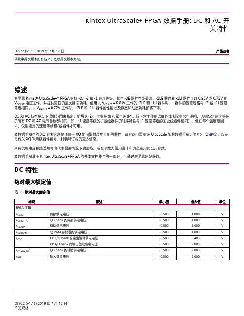
综述赛灵思 Kintex ® UltraScale+™ FPGA 支持 -3、-2 和 -1 速度等级,其中 -3E 器件性能最高。
-2LE 器件和 -1LI 器件可以 0.85V 或 0.72V 的V CCINT 电压工作,并提供更低的最大静态功耗。
使用以 V CCINT = 0.85V 工作的 -2LE 和 -1LI 器件时,L 器件的速度规格与 -2I 或 -1I 速度等级相同。
以 V CCINT = 0.72V 工作时,-2LE 和 -1LI 器件的性能以及静态和动态功耗都将下降。
DC 和 AC 特性按以下温度范围来指定:扩展级 (E)、工业级 (I) 和军工级 (M)。
除正常工作的温度外或者除非另行说明,否则特定速度等级的所有 DC 和 AC 电气参数都相同(即,-1 速度等级的扩展级器件的时序特性与 -1 速度等级的工业级器件相同)。
但在每个温度范围内,仅限选定的速度等级和/或器件才可用。
本数据手册中的 XQ 参考信息仅适用于 XQ 加固型封装中可用的器件。
请参阅《军用级 UltraScale 架构数据手册:简介》 (DS895),以获取有关 XQ 军用级器件编号、封装和订购的更多信息。
所有供电电压和结温规格均代表最差情况下的规格。
所含参数为常用设计和典型应用的公用参数。
本数据手册属于 Kintex UltraScale+ FPGA 的整体文档集合的一部分,可通过赛灵思网站获取。
DC 特性绝对最大额定值Kintex UltraScale+ FPGA 数据手册: DC 和 AC 开关特性条款中英文版本如有歧义,概以英文版本为准。
表 18:LVDS_25 DC 规格标识DC 参数最小值典型值最大值单位V CCO1供电电压 2.375 2.500 2.625V1003506002mV V IDIFF差分输入电压:(Q - Q), Q = High(Q - Q), Q = HighV ICM输入共模电压0.300 1.200 1.425V 注释:1.HD I/O bank 中的 LVDS_25 仅支持输入。
NANO_LX16 FPGA板资料
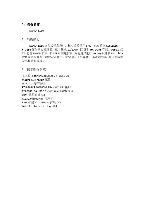
1、设备名称NANO_LX162、功能描述NANO_LX16嵌入式开发套件,核心芯片采用SPARTAN6系列XC6SLX16 FTG256作为核心处理器,板卡集成10/100M千兆网PHY,DDR3存储,USB2.0接口,包含PMOD扩展,和40PIN高速扩展,方便用户进行Verilog设计和Microblze 软核系统级开发,硬件设计精小,非常适合于多媒体,自动化控制,通信领域以及高校教育领域。
3、技术指标参数主芯片Spartan6XC6SLX16-FTQ2562CM25P64SPI FLASH配置DDR22G内存颗粒RTL8201CP10/100M PHY芯片MII接口CY7C68013A USB2.0芯片micro-USB接口50M系统时钟×2RS232,microUART双串口RM3扩展×1PMOD扩展×3Led×8Swith×4keys×44、实物图片图4.1NANO_LX16实物图5、系统框图图5.1NANO_lx16系统框图6、应用领域无线通信智能汽车航空航天消费电子工业自动化7、选配模块7.1RM3模块RM3-AD4高速AD/DA模块可与核心平台配合完成高速数据采集与信号发生方面的设计。
可与核心平台配合完成高速数据采集与信号发生方面的设计。
如DDS函数信号发生器设计、存储示波器设计、基于MATLAB/DSP Builder的系统设计等。
芯片型号:1.AD:AD92012.DA:DAC900U3.运放:8062A主要参数:1.165MHz转换时钟率高速10位DAC;2.20MHz双通道高速10位ADC X2,双通道可实现同时工作,最低功耗215mW;3.AD输入端由275MHz高速集成双路运算放大器隔离,摆率为900V/ms;4.AD输入端输入电压范围0~1伏,1伏直流偏置;5.DA输出端由400M的RF变压器隔离,输出电压范围-250mv~250mv图7.1RM3-AD4实物图图7.2RM3-AD4搭配到NANO_LX16板RM3-LCDRM3接口LCD3.5寸触摸屏,可以与NANO板集成开发有关视频类应用,实现触摸信号的识别和低分辨率视频的处理及显示。
FPGA可编程逻辑器件芯片XC6SLX16-2CSG324I中文规格书
Spartan-6 FPGA Electrical CharacteristicsSpartan®-6 LX and LXT FPGAs are available in various speed grades, with -3 having the highest performance. The DC and AC electrical parameters of the Automotive XA Spartan-6 FPGAs and Defense-grade Spartan-6Q FPGAs devices are equivalent to the commercial specifications except where noted. The timing characteristics of the commercial (XC) -2 speed grade industrial device are the same as for a -2 speed grade commercial device. The -2Q and -3Q speed grades areexclusively for the expanded (Q) temperature range. The timing characteristics are equivalent to those shown for the -2 and -3 speed grades for the Automotive and Defense-grade devices.Spartan-6FPGA DC and AC characteristics are specified for commercial (C), industrial (I), and expanded (Q) temperature ranges. Only selected speed grades and/or devices might be available in the industrial or expanded temperature ranges for Automotive and Defense-grade devices. References to device names refer to all available variations of that part number (for example, LX75 could denote XC6SLX75, XA6SLX75, or XQ6SLX75). The Spartan-6 FPGA -3N speed grade designates devices that do not support MCB functionality.All supply voltage and junction temperature specifications are representative of worst-case conditions. The parameters included are common to popular designs and typical applications. Available device and package combinations can be found at:•DS160: Spartan-6 Family Overview•DS170: Automotive XA Spartan-6 Family Overview •DS172: Defense-Grade Spartan-6Q Family OverviewThis Spartan-6 FPGA data sheet, part of an overall set of documentation on the Spartan-6 family of FPGAs, is available on the Xilinx website at.Spartan-6 FPGA DC CharacteristicsDS162 (v3.1.1) January 30, 2015Product SpecificationTable 1:Absolute Maximum Ratings (1)Symbol DescriptionUnits V CCINT Internal supply voltage relative to GND –0.5 to 1.32V V CCAUX Auxiliary supply voltage relative to GND –0.5 to 3.75V V CCO Output drivers supply voltage relative to GND–0.5 to 3.75V V BATT Key memory battery backup supply (LX75, LX75T, LX100, LX100T , LX150, and LX150T only)–0.5 to 4.05V V FS External voltage supply for eFUSE programming (LX75, LX75T , LX100, LX100T, LX150, and LX150T only)(2)–0.5 to 3.75V V REFInput reference voltage–0.5 to 3.75V找FPGA 和CPLD 可编程逻辑器件,上深圳宇航军工半导体有限公司DCM Switching CharacteristicsTable 53:Operating Frequency Ranges and Conditions for the Delay-Locked Loop (DLL)(1)Symbol DescriptionSpeed GradeUnits -3-3N-2-1LMin Max Min Max Min Max Min MaxLOCK_DLL(3)When using the DLL alone: The timefrom deassertion at the DCM’s resetinput to the rising transition at itsLOCKED output. When the DCM islocked, the CLKIN and CLKFBsignals are in phase.CLKIN_FREQ_DLL <50MHz.–5–5–5–5msWhen using the DLL alone: The timefrom deassertion at the DCM’s resetinput to the rising transition at itsLOCKED output. When the DCM islocked, the CLKIN and CLKFBsignals are in phase.CLKIN_FREQ_DLL >50MHz–0.60–0.60–0.60–0.60ms Delay LinesDCM_DELAY_STEP(5)Finest delay resolution, averagedover all steps.1040104010401040psTable 54:Switching Characteristics for the Delay-Locked Loop (DLL)(1)(Cont’d)Symbol DescriptionSpeed GradeUnits -3-3N-2-1LMin Max Min Max Min Max Min MaxTable 56:Switching Characteristics for the Digital Frequency Synthesizer (DFS) for DCM_SP(1)Symbol DescriptionSpeed GradeUnits -3-3N-2-1LMin Max Min Max Min Max Min MaxOutput Frequency RangesCLKOUT_FREQ_FX Frequency for the CLKFX andCLKFX180 outputs5375537553335200MHzOutput Clock Jitter(2)(3)CLKOUT_PER_JITT_FX Period jitter at the CLKFX andCLKFX180 outputs. WhenCLKIN<20MHzUse the Clocking Wizard psPeriod jitter at the CLKFX andCLKFX180 outputs. WhenCLKIN>20MHzT ypical=±(1%of CLKFX period+100)psDuty Cycle(4)(5)CLKOUT_DUTY_CYCLE_FX Duty cycle precision for the CLKFXand CLKFX180 outputs including theBUFGMUX and clock tree duty-cycledistortionMaximum=±(1%of CLKFX period+350)psPhase Alignment (Phase Error)(5)CLKOUT_PHASE_FX Phase offset between the DFSCLKFX output and the DLL CLK0output when both the DFS and DLLare used–±200–±200–±200–±250psCLKOUT_PHASE_FX180Phase offset between the DFSCLKFX180 output and the DLL CLK0output when both the DFS and DLLare usedMaximum=±(1%of CLKFX period+200)psLOCKED TimeLOCK_FX(2)When FCLKIN<50MHz, the timefrom deassertion at the DCM’s resetinput to the rising transition at itsLOCKED output. The DFS assertsLOCKED when the CLKFX andCLKFX180 signals are valid. Whenusing both the DLL and the DFS, usethe longer locking time.–5–5–5–5msWhen FCLKIN>50 MHz, the timefrom deassertion at the DCM’s resetinput to the rising transition at itsLOCKED output. The DFS assertsLOCKED when the CLKFX andCLKFX180 signals are valid. Whenusing both the DLL and the DFS, usethe longer locking time.–0.45–0.45–0.45–0.60msNotes:1.The values in this table are based on the operating conditions described in T able2 and T able55.2.For optimal jitter tolerance and a faster LOCK time, use the CLKIN_PERIOD attribute.3.Output jitter is characterized with no input jitter. Output jitter strongly depends on the environment, including the number of SSOs, the output drivestrength, CLB utilization, CLB switching activities, switching frequency, power supply, and PCB design. The actual maximum output jitter depends on the system application.4.The CLKFX, CLKFXDV, and CLKFX180 outputs have a duty cycle of approximately 50%.5.Some duty cycle and alignment specifications include a percentage of the CLKFX output period. For example, this data sheet specifies a maximumCLKFX jitter of ±(1%of CLKFX period+200ps). Assuming that the CLKFX output frequency is 100MHz, the equivalent CLKFX period is 10ns, and 1% of 10ns is 0.1ns or 100ps. Accordingly, the maximum jitter is ±(100ps+200ps)=±300ps.。
FPGA可编程逻辑器件芯片XCZU6CG-2FFVC900E中文规格书
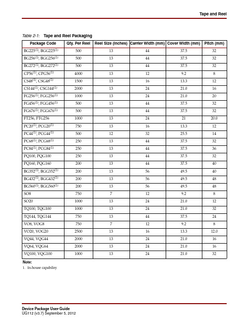
Device Package User Guide UG112 (v3.7) September 5, 2012Tape and ReelTable 2-1:Tape and Reel PackagingPackage Code Qty. Per Reel Reel Size (inches)Carrier Width (mm)Cover Width (mm) Pitch (mm) BG225(1), BGG225(1)500134437.532BG256(1), BGG256(1)500134437.532BG272(1), BGG272(1)500134437.532CP56(1), CPG56(1)400013129.28CS48(1), CSG48(1)1500131613.312CS144(1), CSG144(1)2000132421.016FG256(1), FGG256(1)1000132421.020FG456(1), FGG456(1)500134437.532FG676(1), FGG676(1)500134437.532FT256, FTG256100013242120.0 PC20(1), PCG20(1)750131613.312PC44(1), PCG44(1)500123225.514PC68(1), PCG68(1)250134437.532PC84(1), PCG84(1)250134437.536PQ100, PQG100250134437.532PQ160, PQG160200134437.540BG352(1), BGG352(1)200135649.540BG432(1), BGG432(1)200135649.548BG560(1), BGG560(1)200135649.548SO87507129.28SO201000132421.012TQ100, TQG1001000132421.032TQ144, TQG144750134437.524VO8, VOG87507129.28VO20, VOG202500131613.312.0 VQ44, VQG442000132421.016VQ64, VQG642000132421.016VQ100, VQG1001000132421.032Note:1.In-house capability.Device Package User Guide UG112 (v3.7) September 5, 2012Chapter 3:Thermal Management & Thermal Characterization Methods & ConditionsA copper heatsink plate at the top of the package is used in θJC methods to achieve the forced preferred directional flow.Prior to 1999, the junction-to-case characterization on some heatsink packages wasaccomplished in a 3M Flourinert (FC-40) isothermal circulating fluid stabilized at 25°C. Current Xilinx data on θJC is simulated using the cold plate approach.Prior to 2010, The JEDEC standard proposed to use thermocouples to measure T C . The new JEDEC standard JESD51-14 does not include the measurement of case temperature.Instead, it describes the transient dual interface (TDI) test method for the measurement of the junction-to-case thermal resistance.From the previous JEDEC standards, with applied power (P D ) and under stabilized conditions, case temperature (T C ) is measured with a low gauge thermocouple (36-40 AWG) at the primary heat-flow path of the particular package. Junction temperature (T J ) is calculated from the diode forward-voltage drop from the initial stable condition before power is applied:θJC = (T J – T C )/P Dwhere the terms are as defined above. A poorly defined θJC condition usually leads to lower numbers being reported. In such cases, the recorded temperature difference (T J -T C ) is the result of having a fraction of the power going through the path. However, in the calculation, the full power is used.Because the necessary thermocouple measurement of the case temperature is prone to errors, these results are often not sufficiently reproducible. Some of the errors that could occur are:• A temperature distribution at the package case while the thermocouple measures thetemperature at its contact point to the case. This might not be the maximum case temperature.• A potentially low case temperature reading because the thermocouple beads are often not sufficiently insulated against the cold plate and could therefore be cooled from the wire and cold plate side.•The application of considerable clamping pressure to press the semiconductor device against the heatsink, which closes delaminations.•The drill hole for the thermocouple in the heatsink influencing the thermocouple measurement. This influence increases with smaller devices.Figure 3-9:θJCMeasurement SetupUG112_C3_03_111208。
FPGA可编程逻辑器件芯片XC6VLX365T-2FFG1156C中文规格书

Thermal SpecificationsSummaryThis chapter provides thermal data associated with Virtex®-5 FPGA packages. Thefollowing topics are discussed:•Introduction•Power Management Strategy•Some Thermal Management Options•Support for Compact Thermal Models (CTM)•ReferencesIntroductionVirtex-5 devices are offered exclusively in thermally efficient flip-chip BGA packages.These 1.0 mm flip-chip packages range in pin-count from the smaller 19x19mm FF324 tothe 42.5x42.5mm FF1760. The suite of packages is used to address the various powerrequirements of the Virtex-5devices. All Virtex-5 devices are implemented in the 65nmprocess technologySimilar to Virtex-4 FPGAs, all Virtex-5 devices feature versatile SelectIO™ resources thatsupport a variety of I/O standards. They also include Digital Clock Managers (DCMs),DSPs, and other traditional features and blocks (such as block RAM) contained in earlierVirtex products.In line with Moore's law, the transistor count in this family of devices has been increasedsubstantially. Though several innovative features at the silicon level have been deployed tominimize power dissipation, including leakage at the 65nm node, these products havemore densely packed transistors and embedded blocks with the capability to run fasterthan before. Thus, a fully configured Virtex-5 design that exploits the fabric speed andincorporates several embedded circuits and systems can present power consumptionchallenges that must be managed.Unlike features in an ASIC or a microprocessor, the combination of FPGA features used inan user application are not known to the component supplier. Therefore, it remains achallenge for Xilinx to predict the power requirements of a given FPGA when it leaves thefactory. Accurate estimates are obtained when the board design takes shape. For thispurpose, Xilinx offers and supports a suite of integrated device power analysis tools tohelp users quickly and accurately estimate their design power requirements. Virtex-5devices are supported similarly to previous FPGA products. The uncertainty of designpower requirements makes it difficult to apply canned thermal solutions to fit all users.Therefore, Xilinx devices do not come with preset thermal solutions. The user’s operatingconditions dictate the appropriate solution.Power Management Strategy•Heat Sinking Solutions at the System LevelDepending on the system's physical as well as mechanical constraints, the expectation is that the thermal budget is maintained with custom or OEM heat sink solutions,providing the third prong in the thermal management strategy. At this point, Xilinx has left the heat sink solution to the system-level designers who can tailor the design and solution to the constraints of their systems, being fully aware that the part has certain inherent capabilities for delivering the heat to the surface.Heat sink solutions do exist and can be effective on these low θJB flip-chip platforms.Table 6-3 below illustrates a finned heat sink solution matrix in Network environment (1U and 2U) arrangement for 35mm packages and up for power ranging from 15W to 40W. The AAVID standard finned heat sink offerings are used to illustrate the coverage given thermal budgets of ΔT =35°C and ΔT =45°C scenarios. Other heat sink configurations can be explored similarly.The Virtex-5 FPGA packages can be grouped into medium- and high-performancepackages based on their power handling capabilities. All Virtex-5 FPGA packages can use thermal enhancements, ranging from simple airflow to schemes that can include passive as well as active heat sinks. This is particularly true for the bigger flip-chip BGA packages where system designers have the option to further enhance the packages with bigger and more elaborate heat sinks to handle excesses of 25W with arrangements that consider system –physical constraints as illustrated in Table 6-3.Table 6-3:Finned Heat Sink Solution Matrix for Large Flip-chip BGA in Network Package Power(W)35 x 35 mmFF1136/FF1153/FF115642.5 x 42.5 mmFF1738/FF1759/FF1760ΔT=35°CΔT=45°CΔT=35°CΔT=45°C15W1U (5)Note 1Note 12U (6)Note 1Note 125W1U (5)Note 4Note 2Note 4Note 22U (6)Note 2Note 1Note 2Note 135W1U (5)Note 4Note 3Note 4Note 32U (6)Note 4Note 2Note 4Note 240W1U (5)––Note 4Note 32U (6)Note 3Note 2Notes:1.Solution available at 200 LFM, for example, AAVID finned part number 68520, 72390, 72415.2.Solution available at 400 LFM, for example, AAVID finned part number 68520, 69920.3.Solution available at 600 LFM, for example, AAVID finned part number 72390, 69920, 74590.4.No standard. AAVID finned solution below 600 LFM—custom finned might be required.5.For 1U Height—(max heat sink height = 26mm)6.For 2U Height—(max heat sink height = 64mmChapter 6:Thermal SpecificationsThe flip-chip thermal management chart in Figure6-2 illustrates simple but incrementalpower management schemes that can be applied on a flip-chip BGA package.FF665, FFG665, EF665, FFV665 Flip-Chip Fine-PitchBGA Package Specifications (1.00mm Pitch)Figure 4-3: FF665, FFG665, EF665, FFV665 Flip-Chip Fine-Pitch BGA Package SpecificationsEF1738 Flip-Chip Fine-Pitch BGA Package Specifications (1.00mm Pitch)Figure 4-9:EF1738 Flip-Chip Fine-Pitch BGA Package Specifications。
FPGA可编程逻辑器件芯片XC6SLX9-2FTG256C中文规格书
Spartan-6 FPGA Electrical CharacteristicsSpartan®-6 LX and LXT FPGAs are available in various speed grades, with -3 having the highest performance. The DC and AC electrical parameters of the Automotive XA Spartan-6 FPGAs and Defense-grade Spartan-6Q FPGAs devices are equivalent to the commercial specifications except where noted. The timing characteristics of the commercial (XC) -2 speed grade industrial device are the same as for a -2 speed grade commercial device. The -2Q and -3Q speed grades areexclusively for the expanded (Q) temperature range. The timing characteristics are equivalent to those shown for the -2 and -3 speed grades for the Automotive and Defense-grade devices.Spartan-6FPGA DC and AC characteristics are specified for commercial (C), industrial (I), and expanded (Q) temperature ranges. Only selected speed grades and/or devices might be available in the industrial or expanded temperature ranges for Automotive and Defense-grade devices. References to device names refer to all available variations of that part number (for example, LX75 could denote XC6SLX75, XA6SLX75, or XQ6SLX75). The Spartan-6 FPGA -3N speed grade designates devices that do not support MCB functionality.All supply voltage and junction temperature specifications are representative of worst-case conditions. The parameters included are common to popular designs and typical applications. Available device and package combinations can be found at:•DS160: Spartan-6 Family Overview•DS170: Automotive XA Spartan-6 Family Overview •DS172: Defense-Grade Spartan-6Q Family OverviewSpartan-6 FPGA DC CharacteristicsSpartan-6 FPGA Data Sheet:DC and Switching CharacteristicsDS162 (v3.1.1) January 30, 2015Product SpecificationTable 1:Absolute Maximum Ratings (1)Symbol DescriptionUnits V CCINT Internal supply voltage relative to GND –0.5 to 1.32V V CCAUX Auxiliary supply voltage relative to GND –0.5 to 3.75V V CCO Output drivers supply voltage relative to GND–0.5 to 3.75V V BATT Key memory battery backup supply (LX75, LX75T, LX100, LX100T , LX150, and LX150T only)–0.5 to 4.05V V FS External voltage supply for eFUSE programming (LX75, LX75T , LX100, LX100T, LX150, and LX150T only)(2)–0.5 to 3.75V V REFInput reference voltage–0.5 to 3.75VSymbol DescriptionSpeed Grade Units(Min) -3-3N-2-1LDNA_CYCLES Number of DNA_PORT READ operations or JT AG ISC_DNA read command operations. Unaffected by SHIFT operations.30,000,000ReadCyclesAES_CYCLES Number of JTAG FUSE_KEY or FUSE_CNTL read command operations.Unaffected by SHIFT operations.30,000,000ReadCyclesSymbol Description MIn Max Units MGTAVCC Analog supply voltage for the GTP transmitter and receiver circuits relative toGND–0.5 1.32VMGTAVTTTX Analog supply voltage for the GTP transmitter termination circuit relative to GND–0.5 1.32V MGT AVTTRX Analog supply voltage for the GTP receiver termination circuit relative to GND–0.5 1.32V MGTAVCCPLL Analog supply voltage for the GTP transmitter and receiver PLL circuits relative toGND–0.5 1.32VMGTAVTTRCAL Analog supply voltage for the resistor calibration circuit of the GTP transceiverbank (top or bottom)–0.5 1.32V V IN Receiver (RXP/RXN) and Transmitter (TXP/TXN) absolute input voltage–0.5 1.32V V MGTREFCLK Reference clock absolute input voltage–0.5 1.32VNotes:1.Stresses beyond those listed under Absolute Maximum Ratings might cause permanent damage to the device. These are stress ratings only, andfunctional operation of the device at these or any other conditions beyond those listed under Operating Conditions is not implied. Exposure to Absolute Maximum Ratings conditions for extended periods of time might affect device reliability.Symbol Description Min Typ Max Units MGT AVCC Analog supply voltage for the GTP transmitter and receiver circuits relative to GND 1.14 1.20 1.26V MGT AVTTTX Analog supply voltage for the GTP transmitter termination circuit relative to GND 1.14 1.20 1.26V MGTAVTTRX Analog supply voltage for the GTP receiver termination circuit relative to GND 1.14 1.20 1.26V MGTAVCCPLL Analog supply voltage for the GTP transmitter and receiver PLL circuits relative toGND1.14 1.20 1.26VMGT AVTTRCAL Analog supply voltage for the resistor calibration circuit of the GTP transceiverbank (top or bottom)1.14 1.20 1.26VTable 14:GTP Transceiver Current Supply (per Lane)Symbol DescriptionTyp (1)Max Units I MGTAVCC GTP transceiver internal analog supply current 40.4Note 2mA I MGTAVTTTXGTP transmitter termination supply current 27.4mA I MGTAVTTRX GTP receiver termination supply current 13.6mA I MGTAVCCPLL GTP transmitter and receiver PLL supply current28.7mA R MGTRREFPrecision reference resistor for internal calibration termination50.0 ±1% toleranceΩNotes:1.T ypical values are specified at nominal voltage, 25°C, with a2.5Gb/s line rate, with a shared PLL use mode.2.Values for currents of other transceiver configurations and conditions can be obtained by using the Xilinx Power Estimator (XPE) or Xilinx PowerAnalyzer (XP A) tools.Table 15:GTP Transceiver Quiescent Supply Current (per Lane)(1)(2)(3)(4)Symbol DescriptionTyp (5)Max Units I MGTAVCCQ Quiescent MGTAVCC supply current 1.7Note 2mA I MGTAVTTTXQ Quiescent MGTAVTTTX supply current 0.1mA I MGTAVTTRXQQuiescent MGTAVTTRX supply current1.2mA I MGTAVCCPLLQ Quiescent MGTAVCCPLL supply current1.0mAOutput Delay MeasurementsOutput delays are measured using a Tektronix P6245TDS500/600 probe (<1pF) across approximately 4" of FR4 microstrip trace. Standard termination was used for all testing. The propagation delay of the 4" trace ischaracterized separately and subtracted from the final measurement, and is therefore not included in thegeneralized test setups shown in Figure 4 and Figure 5.Measurements and test conditions are reflected in the IBIS models except where the IBIS format precludes it.Parameters V REF , R REF , C REF , and V MEAS fully describe the test conditions for each I/O standard. The most accurate prediction of propagation delay in any given application can be obtained through IBIS simulation, using the following method:1.Simulate the output driver of choice into the generalizedtest setup, using values from T able 32.2.Record the time to V MEAS .3.Simulate the output driver of choice into the actual PCBtrace and load, using the appropriate IBIS model or capacitance value to represent the load.4.Record the time to V MEAS .pare the results of steps 2 and 4. The increase ordecrease in delay yields the actual propagation delay of the PCB trace.Figure 4:Single-Ended Test SetupFigure 5:Differential Test SetupTable 32:Output Delay Measurement MethodologyDescriptionI/O Standard AttributeR REF (Ω)C REF (1)(pF)V MEAS (V)V REF (V)LVTTL (Low-Voltage T ransistor-T ransistor Logic)LVTTL (all)1M 0 1.40LVCMOS (Low-Voltage CMOS), 3.3V LVCMOS331M 0 1.650LVCMOS, 2.5V LVCMOS251M 0 1.250LVCMOS, 1.8V LVCMOS181M 00.90LVCMOS, 1.5V LVCMOS151M 00.750LVCMOS, 1.2VLVCMOS121M 00.60PCI (Peripheral Component Interface)33MHz and 66MHz, 3.3VPCI33_3, PCI66_3 (rising edge)2510(2)0.940PCI33_3, PCI66_3 (falling edge)2510(2) 2.03 3.3HSTL (High-Speed Transceiver Logic), Class I HSTL_I 500V REF 0.75HSTL, Class II HSTL_II 250V REF 0.75HSTL, Class III HSTL_III 5000.9 1.5HSTL, Class I, 1.8V HSTL_I_18500V REF 0.9HSTL, Class II, 1.8V HSTL_II_18250V REF 0.9HSTL, Class III, 1.8VHSTL_III_18500 1.1 1.8SSTL (Stub Series Terminated Logic), Class I, 1.8V SSTL18_I 500V REF 0.9SSTL, Class II, 1.8V SSTL18_II 250V REF 0.9SSTL, Class I, 2.5VSSTL2_I50V REF1.25SSTL, Class II, 2.5V SSTL2_II 250V REF 1.25SSTL, Class II, 1.5VSSTL15_II250V REF 0.75LVDS (Low-Voltage Differential Signaling), 2.5V & 3.3V LVDS_25, LVDS_3310000(3)–BLVDS (Bus LVDS), 2.5V BLVDS_25Note 400(3)–Mini-LVDS, 2.5V & 3.3VMINI_LVDS_25, MINI_LVDS_3310000(3)–RSDS (Reduced Swing Differential Signaling), 2.5V & 3.3V RSDS_25, RSDS_3310000(3)–TMDS (Transition Minimized Differential Signaling), 3.3V TMDS_33Note 500(3)–PPDS (Point-to-Point Differential Signaling, 2.5V & 3.3VPPDS_25, PPDS_331000(3)–DescriptionI/O Standard Attribute R REF (Ω)C REF (1)(pF)V MEAS (V)V REF (V)。
FPGA可编程逻辑器件芯片XC6SLX9-2CSG225C中文规格书
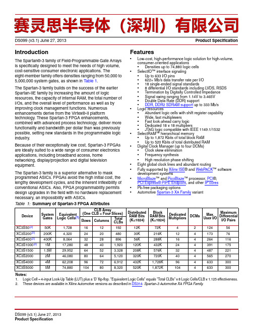
IntroductionThe Spartan®-3 family of Field-Programmable Gate Arrays is specifically designed to meet the needs of high volume, cost-sensitive consumer electronic applications. Theeight-member family offers densities ranging from 50,000 to 5,000,000 system gates, as shown in Table 1.The Spartan-3 family builds on the success of the earlier Spartan-IIE family by increasing the amount of logicresources, the capacity of internal RAM, the total number of I/Os, and the overall level of performance as well as by improving clock management functions. Numerous enhancements derive from the Virtex®-II platform technology. These Spartan-3 FPGA enhancements,combined with advanced process technology, deliver more functionality and bandwidth per dollar than was previously possible, setting new standards in the programmable logic industry.Because of their exceptionally low cost, Spartan-3 FPGAs are ideally suited to a wide range of consumer electronics applications, including broadband access, home networking, display/projection and digital television equipment.The Spartan-3 family is a superior alternative to mask programmed ASICs. FPGAs avoid the high initial cost, the lengthy development cycles, and the inherent inflexibility of conventional ASICs. Also, FPGA programmability permits design upgrades in the field with no hardware replacement necessary, an impossibility with ASICs.Features•Low-cost, high-performance logic solution for high-volume,consumer-oriented applications •Densities up to 74,880 logic cells •SelectIO™ interface signaling •Up to 633 I/O pins •622+ Mb/s data transfer rate per I/O •18 single-ended signal standards •8 differential I/O standards including LVDS, RSDS •Termination by Digitally Controlled Impedance •Signal swing ranging from 1.14V to 3.465V •Double Data Rate (DDR) support •DDR, DDR2 SDRAM support up to 333Mb/s •Logic resources •Abundant logic cells with shift register capability •Wide, fast multiplexers •Fast look-ahead carry logic •Dedicated 18 x 18 multipliers •JT AG logic compatible with IEEE 1149.1/1532•SelectRAM™ hierarchical memory •Up to 1,872 Kbits of total block RAM •Up to 520 Kbits of total distributed RAM •Digital Clock Manager (up to four DCMs)•Clock skew elimination •Frequency synthesis •High resolution phase shifting•Eight global clock lines and abundant routing•Fully supported by Xilinx ISE ® and WebP ACK ™ software development systems•MicroBlaze ™ and PicoBlaze ™ processor, PCI ®,PCI Express® PIPE Endpoint , and other IP cores •Pb-free packaging options•Automotive Spartan-3 XA Family variantDS099 (v3.1) June 27, 2013Product SpecificationTable 1:Summary of Spartan-3 FPGA AttributesDeviceSystem Gates EquivalentLogic Cells (1)CLB Array(One CLB = Four Slices)Distributed RAM Bits (K=1024)BlockRAM Bits (K=1024)DedicatedMultipliersDCMsMax.User I/OMaximumDifferentialI/O Pairs Rows ColumnsTotalCLBs XC3S50(2)50K 1,728161219212K 72K 4212456XC3S200(2)200K 4,320242048030K 216K 12417376XC3S400(2)400K 8,064322889656K 288K 164264116XC3S1000(2)1M 17,28048401,920120K 432K 244391175XC3S1500 1.5M 29,95264523,328208K 576K 324487221XC3S20002M 46,08080645,120320K 720K 404565270XC3S40004M 62,20896726,912432K 1,728K 964633300XC3S50005M74,880104808,320520K1,872K1044633300Notes:1.Logic Cell = 4-input Look-Up T able (LUT) plus a ‘D’ flip-flop. "Equivalent Logic Cells" equals "T otal CLBs" x 8 Logic Cells/CLB x 1.125 effectiveness.2.These devices are available in Xilinx Automotive versions as described in DS314: Spartan-3 Automotive XA FPGA Family .CCLK: Configuration ClockThe configuration clock signal on this pin synchronizes the reading or writing of configuration data. The CCLK pin is an input-only pin for the Slave Serial and Slave Parallel configuration modes. In the Master Serial and Master Parallel configuration modes, the FPGA drives the CCLK pin and CCLK should be treated as a full bidirectional I/O pin for signal integrity analysis.Although the CCLK frequency is relatively low, Spartan-3 FPGA output edge rates are fast. Any potential signal integrity problems on the CCLK board trace can cause FPGA configuration to fail. Therefore, pay careful attention to the CCLK signal integrity on the printed circuit board. Signal integrity simulation with IBIS is recommended. For all configuration modes except JTAG, consider the signal integrity at every CCLK trace destination, including the FPGA’s CCLK pin. For more details on CCLK design considerations, see Chapter 2 of UG332, Spartan-3 Generation Configuration User Guide.During configuration, the CCLK pin has a pull-up resistor to VCCAUX, regardless of the HSWAP_EN pin. After configuration, the CCLK pin is pulled High to VCCAUX by default as defined by the CclkPin bitstream selection, although this behavior is programmable. Any clocks applied to CCLK after configuration are ignored unless the bitstream option Persist is set to Yes, which retains the configuration interface. Persist is set to No by default. However, if Persist is set to Yes, then all clock edges are potentially active events, depending on the other configuration control signals.The bitstream generator option ConfigRate determines the frequency of the internally-generated CCLK oscillator required for the Master configuration modes. The actual frequency is approximate due to the characteristics of the silicon oscillator and varies by up to 50% over the temperature and voltage range. By default, CCLK operates at approximately 6 MHz. Via the ConfigRate option, the oscillator frequency is set at approximately 3, 6, 12, 25, or 50 MHz. At power-on, CCLK always starts operation at its lowest frequency. The device does not start operating at the higher frequency until the ConfigRate control bits are loaded during the configuration process.PROG_B: Program/Configure DeviceThis asynchronous pin initiates the configuration or re-configuration processes. A Low-going pulse resets the configuration logic, initializing the configuration memory. This initialization process cannot finish until PROG_B returns High. Asserting PROG_B Low for an extended period delays the configuration process. At power-up, there is always a pull-up resistor to VCCAUX on this pin, regardless of the HSWAP_EN input. After configuration, the bitstream generator option ProgPin determines whether or not the pull-up resistor is present. By default, the ProgPin option retains the pull-up resistor.After configuration, hold the PROG_B input High. Any Low-going pulse on PROG_B lasting 300ns or longer restarts the configuration process.Table 73:PROG_B OperationDONE: Configuration Done, Delay Start-Up SequenceThe FPGA produces a Low-to-High transition on this pin indicating that the configuration process is complete. The bitstream generator option DriveDone determines whether this pin functions as a totem-pole output that can drive High or as an open-drain output. If configured as an open-drain output—which is the default behavior—then a pull-up resistor is required to produce a High logic level. There is a bitstream option that provides an internal pull-up resistor, otherwise an external pull-up resistor is required.The open-drain option permits the DONE lines of multiple FPGAs to be tied together, so that the common node transitions High only after all of the FPGAs have completed configuration. Externally holding the open-drain DONE pin Low delays the start-up sequence, which marks the transition to user mode.Once the FPGA enters User mode after completing configuration, the DONE pin no longer drives the DONE pin Low. The bitstream generator option DonePin determines whether or not a pull-up resistor is present on the DONE pin to pull the pin to VCCAUX. If the pull-up resistor is eliminated, then the DONE pin must be pulled High using an external pull-up resistor or one of the FPGAs in the design must actively drive the DONE pin High via the DriveDone bitstream generator option.The bitstream generator option DriveDone causes the FPGA to actively drive the DONE output High after configuration. This option should only be used in single-FPGA designs or on the last FPGA in a multi-FPGA daisy-chain.By default, the bitstream generator software retains the pull-up resistor and does not actively drive the DONE pin as highlighted in T able 74, which shows the interaction of these bitstream options in single- and multi-FPGA designs.M2, M1, M0: Configuration Mode SelectionThe M2, M1, and M0 inputs select the FPGA configuration mode, as described in Table 75. The logic levels applied to the mode pins are sampled on the rising edge of INIT_B.Before and during configuration, the mode pins have an internal pull-up resistor to VCCAUX, regardless of the HSWAP_EN pin. If the mode pins are unconnected, then the FPGA defaults to the Slave Serial configuration mode. After configuration successfully completes, any levels applied to these input are ignored. Furthermore, the bitstream generator options M0Pin, M1Pin, and M2Pin determines whether a pull-up resistor, pull-down resistor, or no resistor is present on its respective mode pin, M0, M1, or M2.Table 74:DonePin and DriveDone Bitstream Option InteractionDonePin DriveDoneSingle- or Multi- FPGA DesignCommentsPullnone No Single External pull-up resistor, with value between 330Ω to 3.3k Ω, required on DONE.Pullnone No Multi External pull-up resistor, with value between 330Ω to 3.3k Ω, required on common node connecting to all DONE pins.Pullnone Y es Single OK, no external requirements.Pullnone Y es Multi DriveDone on last device in daisy-chain only. No external requirements.Pullup No Single OK, but pull-up on DONE pin has slow rise time. May require 330Ω pull-up resistor for high CCLK frequencies.Pullup No Multi External pull-up resistor, with value between 330Ω to 3.3k Ω, required on common node connecting to all DONE pins.Pullup Y es Single OK, no external requirements.PullupY esMultiDriveDone on last device in daisy-chain only. No external requirements.Table 75:Spartan-3 FPGA Mode Select SettingsConfiguration Mode M2M1M0Master Serial 000Slave Serial 111Master Parallel 011Slave Parallel 110JTAG 101Reserved 001Reserved 010Reserved100After Configuration XXXNotes:1.X =don’t care, either 0 or 1.Bitstream OptionsTable 80 lists the various bitstream options that affect pins on a Spartan-3 FPGA. The table shows the names of the affected pins, describes the function of the bitstream option, the name of the bitstream generator option variable, and the legal values for each variable. The default option setting for each variable is indicated with bold, underlined text.VCCO: I/O bank output voltage supply pinsVCCO_4(for DUAL pins)Same voltage as external interface Same voltage as external interface Same voltage as external interface Same voltage as external interfaceVCCO_4N/A VCCO_5(for DUAL pins)VCCO_5VCCO_5Same voltage as external interface Same voltage as external interfaceVCCO_5N/A VCCO_#VCCO_#VCCO_#VCCO_#VCCO_#VCCO_#N/AVCCAUX: Auxiliary voltage supply pins VCCAUX+2.5V+2.5V+2.5V+2.5V+2.5VN/AVCCINT+1.2V+1.2V+1.2V+1.2V+1.2VN/AGND GND GND GND GND GND N/ANotes:1.#= I/O bank number, an integer from 0 to 7.2.(I) = input, (O) = output, (OD) = open-drain output, (I/O) = bidirectional, (I/OD) = bidirectional with open-drain output. Open-drain output requires pull-up to create logic High level.3.Shaded cell indicates that the pin is high-impedance during configuration. T o enable a soft pull-up resistor during configuration, drive or tie HSWAP_EN Low.Table 80:Bitstream Options Affecting Spartan-3 Device PinsAffected Pin Name(s)Bitstream Generation FunctionOption Variable Name Values (Default)All unused I/O pins of type I/O, DUAL, GCLK, DCI, VREFFor all I/O pins that are unused in the application after configuration, this option defines whether the I/Os are individually tied to VCCO via a pull-up resistor, tied ground via a pull-down resistor, or left floating. If left floating, the unused pins should be connected to a defined logic level, either from a source internal to the FPGA or external.UnusedPin•Pulldown •Pullup •Pullnone IO_Lxxy_#/DIN, IO_Lxxy_#/DOUT , IO_Lxxy_#/INIT_B Serial configuration mode: If set to Y es, then these pins retain their functionality after configuration completes, allowing for device (re-)configuration. Readback is not supported in with serial mode.Persist•No •Y es IO_Lxxy_#/D0, IO_Lxxy_#/D1, IO_Lxxy_#/D2, IO_Lxxy_#/D3, IO_Lxxy_#/D4, IO_Lxxy_#/D5, IO_Lxxy_#/D6, IO_Lxxy_#/D7, IO_Lxxy_#/CS_B, IO_Lxxy_#/RDWR_B, IO_Lxxy_#/BUSY , IO_Lxxy_#/INIT_BParallel configuration mode (also called SelectMAP): If set to Y es, then these pins retain their SelectMAP functionality after configuration completes, allowing for device readback and for partial or complete (re-)configuration.Persist•No •Y esTable 79:Pin Behavior After Power-Up, During Configuration (Cont’d)Pin NameConfiguration Mode Settings <M2:M1:M0>Bitstream ConfigurationOptionSerial ModesSelectMap Parallel Modes JTAG Mode <1:0:1>Master <0:0:0>Slave <1:1:1>Master <0:1:1>Slave <1:1:0>。
FPGA可编程逻辑器件芯片EPCS16N中文规格书
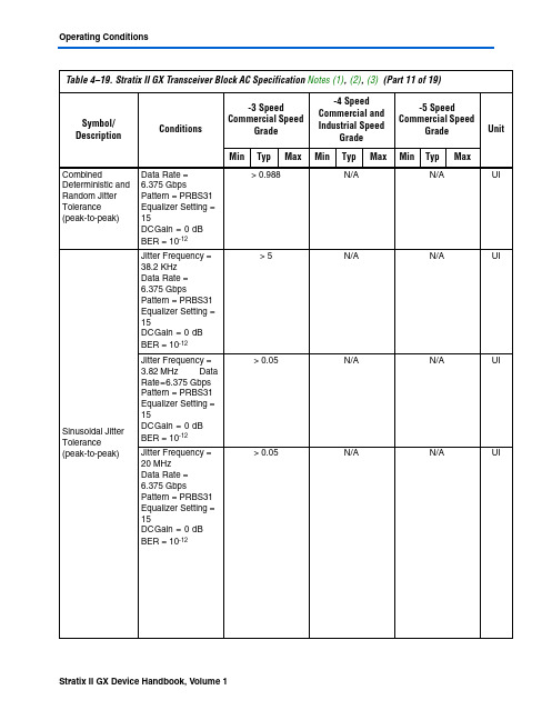
Operating ConditionsCombined Deterministic and Random Jitter Tolerance (peak-to-peak)Data Rate =6.375GbpsPattern=PRBS31Equalizer Setting=15DC G ain =0 dBBER = 10-12>0.988N/A N/A UISinusoidal Jitter Tolerance (peak-to-peak)Jitter Frequency =38.2 KHzData Rate =6.375GbpsPattern=PRBS31Equalizer Setting =15DC G ain = 0d BBER = 10-12>5N/A N/A UIJitter Frequency =3.82 MHz DataRate =6.375GbpsPattern=PRBS31Equalizer Setting =15DC G ain=0d BBER = 10-12>0.05N/A N/A UIJitter Frequency =20 MHzData Rate=6.375GbpsPattern=PRBS31Equalizer Setting =15DC G ain=0d BBER = 10-12>0.05N/A N/A UITable4–19.Stratix II GX Transceiver Block AC Specification Notes(1), (2), (3)(Part 11 of19)Symbol/ Description Conditions-3 SpeedCommercial SpeedGrade-4 SpeedCommercial andIndustrial SpeedGrade-5 SpeedCommercial SpeedGrade Unit Min Typ Max Min Typ Max Min Typ MaxOperating ConditionsTable4–24.LVTTL Specifications(Part 2 of2)Symbol Parameter Conditions Minimum Maximum Unit V OL Low-level output voltage I OL = 4mA (2)0.45V Notes to Table4–24:(1)Stratix II GX devices comply to the narrow range for the supply voltage as specified in the EIA/JEDEC Standard,JESD8-B.(2)This specification is supported across all the programmable drive strength settings available for this I/O standardas shown in the Stratix II GX Architecture chapter in volume 1 of the Stratix II GX Device Handbook.Table4–25.LVCMOS Specifications Note(1)Symbol Parameter Conditions Minimum Maximum Unit V CCIO(1)Output supply voltage 3.135 3.465V V IH High-level input voltage 1.7 4.0V V IL Low-level input voltage–0.30.8V V OH High-level output voltage V CCIO = 3.0, I OH = –0.1mA (2)V CCIO – 0.2V V OL Low-level output voltage V CCIO = 3.0, I OL = 0.1mA (2)0.2V Notes to Table4–25:(1)Stratix II GX devices comply to the narrow range for the supply voltage as specified in the EIA/JEDEC Standard,JESD8-B.(2)This specification is supported across all the programmable drive strength available for this I/O standard as shownin Stratix II GX Architecture chapter in volume 1 of the Stratix II GX Device Handbook.Table4–26.2.5-V I/O SpecificationsSymbol Parameter Conditions Minimum Maximum Unit V CCIO (1)Output supply voltage 2.375 2.625V V IH High-level input voltage 1.7 4.0V V IL Low-level input voltage–0.30.7V V OH High-level output voltage I OH = –1mA (2) 2.0V V OL Low-level output voltage I OL = 1mA (2)0.4V Notes to Table4–26:(1)The Stratix II GX device V CCIO voltage level support of 2.5 to 5% is narrower than defined in the Normal Range ofthe EIA/JEDEC standard.(2)This specification is supported across all the programmable drive settings available for this I/O standard as shownin Stratix II GX Architecture chapter in volume 1 of the Stratix II GX Device Handbook.Timing ModelFinal timing numbers are based on actual device operation and testing.These numbers reflect the actual performance of the device underworst-case voltage and junction temperature conditions.Table4–52.Stratix II GX Device Timing Model StatusDevice Preliminary FinalEP2SGX30vEP2SGX60vEP2SGX90vEP2SGX130vI/O Timing Measurement MethodologyDifferent I/O standards require different baseline loading techniques forreporting timing delays. Altera characterizes timing delays with therequired termination for each I/O standard and with 0pF (except for PCIand PCI-X which use 10pF) loading and the timing is specified up to theoutput pin of the FPGA device. The Quartus II software calculates theI/O timing for each I/O standard with a default baseline loading asspecified by the I/O standards.The following measurements are made during device characterization.Altera measures clock-to-output delays (t CO) at worst-case process,minimum voltage, and maximum temperature (PVT) for default loadingconditions shown in Table4–53. Use the following equations to calculateclock pin to output pin timing for Stratix II GX devices.t CO from clock pin to I/O pin = delay from clock pad to I/O outputregister + IOE output register clock-to-output delay + delayfrom output register to output pin + I/O output delayt xz/t zx from clock pin to I/O pin = delay from clock pad to I/Ooutput register + IOE output register clock-to-output delay +delay from output register to output pin + I/O output delay +output enable pin delaySimulation using IBIS models is required to determine the delays on thePCB traces in addition to the output pin delay timing reported by theQuartus II software and the timing model in the device handbook.1.Simulate the output driver of choice into the generalized test setup,using values from Table4–53.2.Record the time to V MEAS.。
FPGA可编程逻辑器件芯片XC6SLX16-2CSG324I中文规格书

Spartan-6 FPGA Electrical CharacteristicsSpartan®-6 LX and LXT FPGAs are available in various speed grades, with -3 having the highest performance. The DC and AC electrical parameters of the Automotive XA Spartan-6 FPGAs and Defense-grade Spartan-6Q FPGAs devices are equivalent to the commercial specifications except where noted. The timing characteristics of the commercial (XC) -2 speed grade industrial device are the same as for a -2 speed grade commercial device. The -2Q and -3Q speed grades areexclusively for the expanded (Q) temperature range. The timing characteristics are equivalent to those shown for the -2 and -3 speed grades for the Automotive and Defense-grade devices.Spartan-6FPGA DC and AC characteristics are specified for commercial (C), industrial (I), and expanded (Q) temperature ranges. Only selected speed grades and/or devices might be available in the industrial or expanded temperature ranges for Automotive and Defense-grade devices. References to device names refer to all available variations of that part number (for example, LX75 could denote XC6SLX75, XA6SLX75, or XQ6SLX75). The Spartan-6 FPGA -3N speed grade designates devices that do not support MCB functionality.All supply voltage and junction temperature specifications are representative of worst-case conditions. The parameters included are common to popular designs and typical applications. Available device and package combinations can be found at:•DS160: Spartan-6 Family Overview•DS170: Automotive XA Spartan-6 Family Overview •DS172: Defense-Grade Spartan-6Q Family OverviewThis Spartan-6 FPGA data sheet, part of an overall set of documentation on the Spartan-6 family of FPGAs, is available on the Xilinx website at.Spartan-6 FPGA DC CharacteristicsDS162 (v3.1.1) January 30, 2015Product SpecificationTable 1:Absolute Maximum Ratings (1)Symbol DescriptionUnits V CCINT Internal supply voltage relative to GND –0.5 to 1.32V V CCAUX Auxiliary supply voltage relative to GND –0.5 to 3.75V V CCO Output drivers supply voltage relative to GND–0.5 to 3.75V V BATT Key memory battery backup supply (LX75, LX75T, LX100, LX100T , LX150, and LX150T only)–0.5 to 4.05V V FS External voltage supply for eFUSE programming (LX75, LX75T , LX100, LX100T, LX150, and LX150T only)(2)–0.5 to 3.75V V REFInput reference voltage–0.5 to 3.75V找FPGA 和CPLD 可编程逻辑器件,上深圳宇航军工半导体有限公司DCM Switching CharacteristicsTable 53:Operating Frequency Ranges and Conditions for the Delay-Locked Loop (DLL)(1)Symbol DescriptionSpeed GradeUnits -3-3N-2-1LMin Max Min Max Min Max Min MaxLOCK_DLL(3)When using the DLL alone: The timefrom deassertion at the DCM’s resetinput to the rising transition at itsLOCKED output. When the DCM islocked, the CLKIN and CLKFBsignals are in phase.CLKIN_FREQ_DLL <50MHz.–5–5–5–5msWhen using the DLL alone: The timefrom deassertion at the DCM’s resetinput to the rising transition at itsLOCKED output. When the DCM islocked, the CLKIN and CLKFBsignals are in phase.CLKIN_FREQ_DLL >50MHz–0.60–0.60–0.60–0.60ms Delay LinesDCM_DELAY_STEP(5)Finest delay resolution, averagedover all steps.1040104010401040psTable 54:Switching Characteristics for the Delay-Locked Loop (DLL)(1)(Cont’d)Symbol DescriptionSpeed GradeUnits -3-3N-2-1LMin Max Min Max Min Max Min MaxTable 56:Switching Characteristics for the Digital Frequency Synthesizer (DFS) for DCM_SP(1)Symbol DescriptionSpeed GradeUnits -3-3N-2-1LMin Max Min Max Min Max Min MaxOutput Frequency RangesCLKOUT_FREQ_FX Frequency for the CLKFX andCLKFX180 outputs5375537553335200MHzOutput Clock Jitter(2)(3)CLKOUT_PER_JITT_FX Period jitter at the CLKFX andCLKFX180 outputs. WhenCLKIN<20MHzUse the Clocking Wizard psPeriod jitter at the CLKFX andCLKFX180 outputs. WhenCLKIN>20MHzT ypical=±(1%of CLKFX period+100)psDuty Cycle(4)(5)CLKOUT_DUTY_CYCLE_FX Duty cycle precision for the CLKFXand CLKFX180 outputs including theBUFGMUX and clock tree duty-cycledistortionMaximum=±(1%of CLKFX period+350)psPhase Alignment (Phase Error)(5)CLKOUT_PHASE_FX Phase offset between the DFSCLKFX output and the DLL CLK0output when both the DFS and DLLare used–±200–±200–±200–±250psCLKOUT_PHASE_FX180Phase offset between the DFSCLKFX180 output and the DLL CLK0output when both the DFS and DLLare usedMaximum=±(1%of CLKFX period+200)psLOCKED TimeLOCK_FX(2)When FCLKIN<50MHz, the timefrom deassertion at the DCM’s resetinput to the rising transition at itsLOCKED output. The DFS assertsLOCKED when the CLKFX andCLKFX180 signals are valid. Whenusing both the DLL and the DFS, usethe longer locking time.–5–5–5–5msWhen FCLKIN>50 MHz, the timefrom deassertion at the DCM’s resetinput to the rising transition at itsLOCKED output. The DFS assertsLOCKED when the CLKFX andCLKFX180 signals are valid. Whenusing both the DLL and the DFS, usethe longer locking time.–0.45–0.45–0.45–0.60msNotes:1.The values in this table are based on the operating conditions described in T able2 and T able55.2.For optimal jitter tolerance and a faster LOCK time, use the CLKIN_PERIOD attribute.3.Output jitter is characterized with no input jitter. Output jitter strongly depends on the environment, including the number of SSOs, the output drivestrength, CLB utilization, CLB switching activities, switching frequency, power supply, and PCB design. The actual maximum output jitter depends on the system application.4.The CLKFX, CLKFXDV, and CLKFX180 outputs have a duty cycle of approximately 50%.5.Some duty cycle and alignment specifications include a percentage of the CLKFX output period. For example, this data sheet specifies a maximumCLKFX jitter of ±(1%of CLKFX period+200ps). Assuming that the CLKFX output frequency is 100MHz, the equivalent CLKFX period is 10ns, and 1% of 10ns is 0.1ns or 100ps. Accordingly, the maximum jitter is ±(100ps+200ps)=±300ps.。
FPGA可编程逻辑器件芯片XC6SLX45T-2CSG324I中文规格书
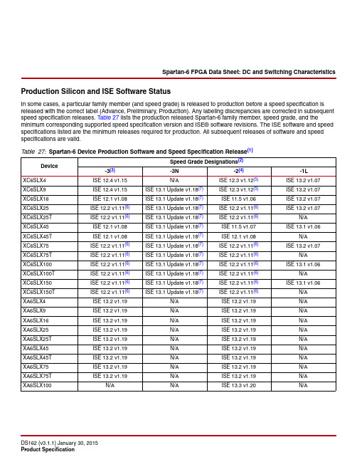
Spartan-6 FPGA Data Sheet: DC and Switching CharacteristicsProduction Silicon and ISE Software StatusIn some cases, a particular family member (and speed grade) is released to production before a speed specification is released with the correct label (Advance, Preliminary, Production). Any labeling discrepancies are corrected in subsequent speed specification releases. Table27 lists the production released Spartan-6 family member, speed grade, and the minimum corresponding supported speed specification version and ISE® software revisions. The ISE software and speed specifications listed are the minimum releases required for production. All subsequent releases of software and speed specifications are valid.Table 27:Spartan-6 Device Production Software and Speed Specification Release(1)DeviceSpeed Grade Designations(2)-3(3)-3N-2(4)-1LXC6SLX4ISE 12.4 v1.15N/A ISE 12.3 v1.12(5)ISE 13.2 v1.07 XC6SLX9ISE 12.4 v1.15ISE 13.1 Update v1.18(7)ISE 12.3 v1.12(5)ISE 13.2 v1.07 XC6SLX16ISE 12.1 v1.08ISE 13.1 Update v1.18(7)ISE 11.5 v1.06ISE 13.2 v1.07 XC6SLX25ISE 12.2 v1.11(6)ISE 13.1 Update v1.18(7)ISE 12.2 v1.11(6)ISE 13.2 v1.07 XC6SLX25T ISE 12.2 v1.11(6)ISE 13.1 Update v1.18(7)ISE 12.2 v1.11(6)N/AXC6SLX45ISE 12.1 v1.08ISE 13.1 Update v1.18(7)ISE 11.5 v1.07ISE 13.1 v1.06 XC6SLX45T ISE 12.1 v1.08ISE 13.1 Update v1.18(7)ISE 12.1 v1.08N/AXC6SLX75ISE 12.2 v1.11(6)ISE 13.1 Update v1.18(7)ISE 12.2 v1.11(6)ISE 13.2 v1.07 XC6SLX75T ISE 12.2 v1.11(6)ISE 13.1 Update v1.18(7)ISE 12.2 v1.11(6)N/AXC6SLX100ISE 12.2 v1.11(6)ISE 13.1 Update v1.18(7)ISE 12.2 v1.11(6)ISE 13.1 v1.06 XC6SLX100T ISE 12.2 v1.11(6)ISE 13.1 Update v1.18(7)ISE 12.2 v1.11(6)N/AXC6SLX150ISE 12.2 v1.11(6)ISE 13.1 Update v1.18(7)ISE 12.2 v1.11(6)ISE 13.1 v1.06 XC6SLX150T ISE 12.2 v1.11(6)ISE 13.1 Update v1.18(7)ISE 12.2 v1.11(6)N/AXA6SLX4ISE 13.2 v1.19N/A ISE 13.2 v1.19N/AXA6SLX9ISE 13.2 v1.19N/A ISE 13.2 v1.19N/AXA6SLX16ISE 13.2 v1.19N/A ISE 13.2 v1.19N/AXA6SLX25ISE 13.2 v1.19N/A ISE 13.2 v1.19N/AXA6SLX25T ISE 13.2 v1.19N/A ISE 13.2 v1.19N/AXA6SLX45ISE 13.2 v1.19N/A ISE 13.2 v1.19N/AXA6SLX45T ISE 13.2 v1.19N/A ISE 13.2 v1.19N/AXA6SLX75ISE 13.2 v1.19N/A ISE 13.2 v1.19N/AXA6SLX75T ISE 13.2 v1.19N/A ISE 13.2 v1.19N/AXA6SLX100N/A N/A ISE 13.3 v1.20N/AXQ6SLX75N/A N/A ISE 13.2 v1.19ISE 13.2 v1.07XQ6SLX75T ISE 13.2 v1.19N/A ISE 13.2 v1.19N/A XQ6SLX150N/A N/A ISE 13.2 v1.19ISE 13.2 v1.07XQ6SLX150TISE 13.2 v1.19N/AISE 13.2 v1.19N/ATable 27:Spartan-6 Device Production Software and Speed Specification Release (1) (Cont’d)DeviceSpeed Grade Designations (2)-3(3)-3N -2(4)-1LI/O Standard Measurement MethodologyInput Delay MeasurementsTable31 shows the test setup parameters used for measuring input delay.Table 31:Input Delay Measurement MethodologyDescription I/O Standard Attribute V L(1)V H(1)V MEAS(3)(4)V REF(2)(4) LVTTL (Low-Voltage T ransistor-T ransistor Logic)LVTTL0 3.0 1.4–LVCMOS (Low-Voltage CMOS), 3.3V LVCMOS330 3.3 1.65–LVCMOS, 2.5V LVCMOS250 2.5 1.25–LVCMOS, 1.8V LVCMOS180 1.80.9–LVCMOS, 1.5V LVCMOS150 1.50.75–LVCMOS, 1.2V LVCMOS120 1.20.6–PCI33_3, PCI66_3Per PCI Specification–PCI (Peripheral Component Interface),33MHz and 66MHz, 3.3VHSTL (High-Speed Transceiver Logic),HSTL_I, HSTL_II V REF–0.5V REF+0.5V REF0.75 Class I & IIHSTL, Class III HSTL_III V REF–0.5V REF+0.5V REF0.90 HSTL, Class I & II, 1.8V HSTL_I_18, HSTL_II_18V REF–0.5V REF+0.5V REF0.90 HSTL, Class III 1.8V HSTL_III_18V REF–0.5V REF+0.5V REF 1.1 SSTL (Stub Terminated Transceiver Logic),SSTL3_I,SSTL3_II V REF–0.75V REF+0.75V REF 1.5 Class I & II, 3.3VSSTL, Class I & II, 2.5V SSTL2_I,SSTL2_II V REF–0.75V REF+0.75V REF 1.25 SSTL, Class I & II, 1.8V SSTL18_I,SSTL18_II V REF–0.5V REF+0.5V REF0.90 SSTL, Class II, 1.5V SSTL15_II V REF–0.2V REF+0.2V REF0.75 LVDS (Low-Voltage Differential Signaling),LVDS_25, LVDS_33 1.25–0.125 1.25+0.1250(5)–2.5V & 3.3VLVPECL (Low-Voltage Positive Emitter-CoupledLVPECL_25, LVPECL_33 1.2–0.3 1.2+0.30(5)–Logic), 2.5V & 3.3VBLVDS (Bus LVDS), 2.5V BLVDS_25 1.3–0.125 1.3+0.1250(5)–1.2–0.125 1.2+0.1250(5)–Mini-LVDS,2.5V &3.3V MINI_LVDS_25,MINI_LVDS_33RSDS_25, RSDS_33 1.2–0.1 1.2+0.10(5)–RSDS (Reduced Swing Differential Signaling),2.5V &3.3VTMDS_33 3.0–0.1 3.0+0.10(5)–TMDS (Transition Minimized Differential Signaling),3.3VPPDS_25, PPDS_33 1.25–0.1 1.25+0.10(5)–PPDS (Point-to-Point Differential Signaling,2.5V &3.3VNotes:1.Input waveform switches between V L and V H.2.Measurements are made at typical, minimum, and maximum V REF values. Reported delays reflect worst case of these measurements. V REF valueslisted are typical.3.Input voltage level from which measurement starts.4.This is an input voltage reference that bears no relation to the V REF / V MEAS parameters found in IBIS models and/or noted in Figure4.5.The value given is the differential input voltage.Output Delay MeasurementsOutput delays are measured using a Tektronix P6245TDS500/600 probe (<1pF) across approximately 4" of FR4 microstrip trace. Standard termination was used for all testing. The propagation delay of the 4" trace ischaracterized separately and subtracted from the final measurement, and is therefore not included in thegeneralized test setups shown in Figure 4 and Figure 5.Measurements and test conditions are reflected in the IBIS models except where the IBIS format precludes it.Parameters V REF , R REF , C REF , and V MEAS fully describe the test conditions for each I/O standard. The most accurate prediction of propagation delay in any given application can be obtained through IBIS simulation, using the following method:1.Simulate the output driver of choice into the generalizedtest setup, using values from T able 32.2.Record the time to V MEAS .3.Simulate the output driver of choice into the actual PCBFigure 5:Differential Test SetupSSTL, Class II, 2.5V SSTL2_II 250V REF 1.25SSTL, Class II, 1.5VSSTL15_II250V REF 0.75LVDS (Low-Voltage Differential Signaling), 2.5V & 3.3V LVDS_25, LVDS_3310000(3)–BLVDS (Bus LVDS), 2.5V BLVDS_25Note 400(3)–Mini-LVDS, 2.5V & 3.3VMINI_LVDS_25, MINI_LVDS_3310000(3)–RSDS (Reduced Swing Differential Signaling), 2.5V & 3.3V RSDS_25, RSDS_3310000(3)–TMDS (Transition Minimized Differential Signaling), 3.3V TMDS_33Note 500(3)–PPDS (Point-to-Point Differential Signaling, 2.5V & 3.3VPPDS_25, PPDS_331000(3)–Table 32:Output Delay Measurement Methodology (Cont’d)DescriptionI/O Standard Attribute R REF (Ω)C REF (1)(pF)V MEAS (V)V REF (V)。
FPGA可编程逻辑器件芯片XC6SLX25T-2CSG324I中文规格书
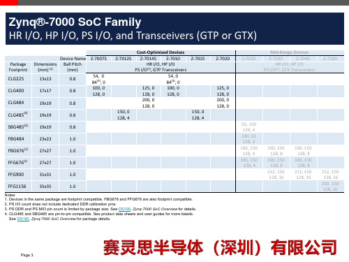
100, 150 128, 8
100, 150 128, 8
212, 150 128, 16
100, 150 128, 8
100, 150 128, 8
212, 150 128, 16
212, 150 128, 16 250, 150 128, 16
Page 3
Zynq®-7000 Family Speed Grades
Zynq®-7000 SoC Family HR I/O, HP I/O, PS I/O, and Transceivers (GTP or GTX)
Package Footprint CLG225
CLG400
CLG484
Device Name
Dimensions Ball Pitch
(mm) (1)
54, 0 84(3), 0
125, 0
100, 0
128, 0
128, 0
200, 0
128, 0
150, 0
128, 4
Z-7015
150, 0 128, 4
FBG484
23x23
1.0
FBG676(1)
27x27
1.0
FFG676(1)
27x27
1.0
FFG900
31x31
1.0
FFG1156
(mm)
13x13
0.8
17x17
0.8
Z-7007S
54, 0 84(3), 0 100, 0 128, 0
19x19
0.8
CLG485(4)
19x19
0.8
SBG485(4)
19x19
0.8
Cost-Optimized Devices
- 1、下载文档前请自行甄别文档内容的完整性,平台不提供额外的编辑、内容补充、找答案等附加服务。
- 2、"仅部分预览"的文档,不可在线预览部分如存在完整性等问题,可反馈申请退款(可完整预览的文档不适用该条件!)。
- 3、如文档侵犯您的权益,请联系客服反馈,我们会尽快为您处理(人工客服工作时间:9:00-18:30)。
Spartan-6 FPGA Electrical CharacteristicsSpartan®-6 LX and LXT FPGAs are available in various speed grades, with -3 having the highest performance. The DC and AC electrical parameters of the Automotive XA Spartan-6 FPGAs and Defense-grade Spartan-6Q FPGAs devices are equivalent to the commercial specifications except where noted. The timing characteristics of the commercial (XC) -2 speed grade industrial device are the same as for a -2 speed grade commercial device. The -2Q and -3Q speed grades areexclusively for the expanded (Q) temperature range. The timing characteristics are equivalent to those shown for the -2 and -3 speed grades for the Automotive and Defense-grade devices.Spartan-6FPGA DC and AC characteristics are specified for commercial (C), industrial (I), and expanded (Q) temperature ranges. Only selected speed grades and/or devices might be available in the industrial or expanded temperature ranges for Automotive and Defense-grade devices. References to device names refer to all available variations of that part number (for example, LX75 could denote XC6SLX75, XA6SLX75, or XQ6SLX75). The Spartan-6 FPGA -3N speed grade designates devices that do not support MCB functionality.All supply voltage and junction temperature specifications are representative of worst-case conditions. The parameters included are common to popular designs and typical applications. Available device and package combinations can be found at:DS162 (v3.1.1) January 30, 2015Product Specification找FPGA,上赛灵思半导体(深圳)有限公司V IN and V TS (3)I/O input voltage or voltage applied to 3-state output, relative to GND (4)All user and dedicatedI/OsCommercialDC–0.60 to 4.10V 20% overshoot duration –0.75 to 4.25V 8% overshoot duration (5)–0.75 to 4.40V IndustrialDC–0.60 to 3.95V 20% overshoot duration –0.75 to 4.15V 4% overshoot duration (5)–0.75 to 4.40V Expanded (Q)DC–0.60 to 3.95V 20% overshoot duration–0.75 to 4.15V 4% overshoot duration (5)–0.75 to 4.40V Restricted tomaximum of 100 user I/OsCommercial20% overshoot duration –0.75 to 4.35V 15% overshoot duration (5)–0.75 to 4.40V 10% overshoot duration–0.75 to 4.45V Industrial 20% overshoot duration –0.75 to 4.25V 10% overshoot duration –0.75 to 4.35V 8% overshoot duration (5)–0.75 to 4.40V Expanded (Q)20% overshoot duration–0.75 to 4.25V 10% overshoot duration–0.75 to 4.35V 8% overshoot duration (5)–0.75 to 4.40V T STGStorage temperature (ambient)–65to 150°C T SOLMaximum soldering temperature (6)(TQG144, CPG196, CSG225, CSG324, CSG484, and FTG256)+260°C Maximum soldering temperature (6) (Pb-free packages: FGG484, FGG676, and FGG900)+250°C Maximum soldering temperature (6) (Pb packages: CS484, FT256, FG484, FG676, and FG900)+220°C T jMaximum junction temperature (6)+125°CNotes:1.Stresses beyond those listed under Absolute Maximum Ratings might cause permanent damage to the device. These are stress ratings only, and functional operation of the device at these or any other conditions beyond those listed under Operating Conditions is not implied.Exposure to Absolute Maximum Ratings conditions for extended periods of time might affect device reliability.2.When programming eFUSE, V FS ≤V CCAUX . Requires up to 40mA current. For read mode, V FS can be between GND and3.45V .3.I/O absolute maximum limit applied to DC and AC signals. Overshoot duration is the percentage of a data period that the I/O is stressed beyond 3.45V .4.For I/O operation, refer to UG381: Spartan-6 FPGA SelectIO Resources User Guide .5.Maximum percent overshoot duration to meet 4.40V maximum.6.T SOL is the maximum soldering temperature for component bodies. For soldering guidelines and thermal considerations,see UG385: Spartan-6 FPGA Packaging and Pinout Specification .Table 1:Absolute Maximum Ratings (1) (Cont’d)SymbolDescriptionUnitseFUSE Read EnduranceTable11 lists the minimum guaranteed number of read cycle operations for Device DNA and for the AES eFUSE key. For more information, see UG380: Spartan-6 FPGA Configuration User Guide.Table 11:eFUSE Read EnduranceSymbol DescriptionSpeed Grade Units(Min) -3-3N-2-1LDNA_CYCLES Number of DNA_PORT READ operations or JT AG ISC_DNA read command operations. Unaffected by SHIFT operations.30,000,000ReadCyclesAES_CYCLES Number of JTAG FUSE_KEY or FUSE_CNTL read command operations.Unaffected by SHIFT operations.30,000,000ReadCyclesSymbol Description Typ(1)Max UnitsI MGTAVCC GTP transceiver internal analog supply current40.4Note2mAI MGTAVTTTX GTP transmitter termination supply current27.4mA I MGTAVTTRX GTP receiver termination supply current13.6mA I MGTAVCCPLL GTP transmitter and receiver PLL supply current28.7mA R MGTRREF Precision reference resistor for internal calibration termination50.0 ±1%toleranceΩGTP Transceiver DC Input and Output LevelsTable 16 summarizes the DC output specifications of the GTP transceivers in Spartan-6 FPGAs. Figure 1 shows the single-ended output voltage swing. Figure 2 shows the peak-to-peak differential output voltage.Consult UG386: Spartan-6 FPGA GTP Transceivers User Guide for further details.Table 17 summarizes the DC specifications of the clock input of the GTP transceiver. Consult UG386: Spartan-6 FPGA GTP Transceivers User Guide for further details.Table 16:GTP Transceiver DC SpecificationsSymbol DC ParameterConditionsMin Typ Max Units DV PPIN Differential peak-to-peak input voltageExternal AC coupled 140–2000mV V IN Absolute input voltage DC coupledMGT AVTTRX =1.2V –400–MGTAVTTRXmV V CMIN Common mode input voltageDC coupledMGTAVTTRX =1.2V–3/4MGTAVTTRX–mV DV PPOUT Differential peak-to-peak output voltage (1)T ransmitter output swing is set to maximum setting 1000––mV V SEOUT Single-ended output voltage swing (1)––500mV V CMOUTDCCommon mode output voltage Equation basedMGTAVTTTX –V SEOUT /2mV R IN Differential input resistance 80100130ΩR OUT Differential output resistance 80100130ΩT OSKEW Transmitter output skew––15ps C EXTRecommended external AC coupling capacitor (2)75100200nFNotes:1.The output swing and preemphasis levels are programmable using the attributes discussed in UG386: Spartan-6 FPGA GTP T ransceivers UserGuide and can result in values lower than reported in this table. DV PPOUT is the minimum guaranteed value at the maximum setting. Refer to UG386:Spartan-6 FPGA GTP Transceivers User Guide for nominal values.2.Other values can be used as appropriate to conform to specific protocols and standards.Figure 1:Single-Ended Peak-to-Peak VoltageFigure 2:Differential Peak-to-Peak Voltage。
