电源完整性分析(于争博士)
于博士信号完整性分析入门(修改)

于博士信号完整性分析入门于争 博士for more information,please refer to 电设计网欢迎您什么是信号完整性?如果你发现,以前低速时代积累的设计经验现在似乎都不灵了,同样的设计,以前没问题,可是现在却无法工作,那么恭喜你,你碰到了硬件设计中最核心的问题:信号完整性。
早一天遇到,对你来说是好事。
在过去的低速时代,电平跳变时信号上升时间较长,通常几个ns。
器件间的互连线不至于影响电路的功能,没必要关心信号完整性问题。
但在今天的高速时代,随着IC输出开关速度的提高,很多都在皮秒级,不管信号周期如何,几乎所有设计都遇到了信号完整性问题。
另外,对低功耗追求使得内核电压越来越低,1.2v内核电压已经很常见了。
因此系统能容忍的噪声余量越来越小,这也使得信号完整性问题更加突出。
广义上讲,信号完整性是指在电路设计中互连线引起的所有问题,它主要研究互连线的电气特性参数与数字信号的电压电流波形相互作用后,如何影响到产品性能的问题。
主要表现在对时序的影响、信号振铃、信号反射、近端串扰、远端串扰、开关噪声、非单调性、地弹、电源反弹、衰减、容性负载、电磁辐射、电磁干扰等。
信号完整性问题的根源在于信号上升时间的减小。
即使布线拓扑结构没有变化,如果采用了信号上升时间很小的IC芯片,现有设计也将处于临界状态或者停止工作。
下面谈谈几种常见的信号完整性问题。
反射:图1显示了信号反射引起的波形畸变。
看起来就像振铃,拿出你制作的电路板,测一测各种信号,比如时钟输出或是高速数据线输出,看看是不是存在这种波形。
如果有,那么你该对信号完整性问题有个感性的认识了,对,这就是一种信号完整性问题。
很多硬件工程师都会在时钟输出信号上串接一个小电阻,至于为什么,他们中很多人都说不清楚,他们会说,很多成熟设计上都有,照着做的。
或许你知道,可是确实很多人说不清这个小小电阻的作用,包括很多有了三四年经验的硬件工程师,很惊讶么?可这确实是事实,我碰到过很多。
电源完整性分析及应用
路设计 中起到至关重要的作用 。
GU Xi a o x u e , GU Di n g f u
( c h i a n E l e c t r o n i c s T e c h n o l o g y Gr o u p C o r p o r a t i o n N o . 5 8 R e s e a r c h I n s t i t u t e , Wu x i 2 1 4 0 7 2 , C h i n a )
中图分 类号 :T N 4 0 2
文献标 识码 :A
文章编号 :1 6 8 1 - 1 0 7 0( 2 0 1 7 )0 2 — 0 0 2 1 - 0 4
Ana l ys i s a n d App l i c a t i o n o f Po we r I n t e g r i t y
nt i e g r i t y , e l e c t r o ma ne g t i c i n t e g r i y t a n d o t h e r s y s t e m i n d i c a t o r s . T h e p a p e r f o c u s e s o n he t p o we r d i s t r i b u t i o n
n e wo t r k a n d t a r g e t i mp e d a n c e me t h o d . S i mu l a t i o n a n a l y s i s o n p o we r i n t e g r i y t i s he t n p e r f o r me d .
一个从业十年的信号完整性讲师给PCB工程师的学习忠告
一个从事PCB信号完整性培训十年的讲师给工程师的建议作者:于争我本人以前就做过多年的信号完整性工程师,现在自己开公司做SI设计咨询,前几年也经常做一些培训(给一家培训公司做讲师),我就从一个讲师的角度来说说我的一点感触!从多次的培训需求征集结果看,需求可以说五花八门,很多工程师或者公司提出的需求归纳起来相当于:一次课程把所有的SI问题搞定。
培训公司为了满足不同客户的需求当然就要把课程的内容作的全一点,覆盖面广一点。
但信号完整性设计那么多内容,2天的时间不可能覆盖到,可以说众口难调。
培训公司也是不得已而为之。
我讲这样的课程也不舒服,总是刚刚接触到一点表面的东西,由于时间关系不得不放弃转入下一个话题,没办法,得赶时间,要不讲不完。
有一句话叫不吐不快,但是在课堂上就是不能尽情的“吐”,有点憋得慌。
工程师对于信号完整性设计也有一个认知过程,很多人一提到信号完整性本能的想到仿真,其实这是一个相当大的认识误区。
每次讲课我都会反复强调,不要把SI设计等同于SI 仿真。
SI仿真只是SI设计的一个环节。
该仿什么?怎么仿?怎么解读仿真结果,怎么判断行不行?怎么做决策?这些不是会操作软件就能搞定的,但这些却正是SI设计最核心的东西。
有人可能会说,导入模型看看波形怎么样不就可以了,呵呵,不用多,真正做一个工程就能有感觉,没这么简单。
单单一个该仿什么,可能就会难倒一大批人,更别说怎么利用仿真结果了。
仿真软件不过是一个工具而已,能不能用好,还要看工程师的知识底蕴。
当然,SI设计不可避免的涉及到测试,这也是一大块比较难的东西,我想做的比较深入的人一定深有体会。
搞SI不能光用软件仿一仿就完事,要做的工作还是很多的。
工程师门提出那些要求其实可以理解,只不过在一次课程中涵盖这些内容不太可能。
我以前也讲过很多次仿真软件的课程,Cadence仿真、Hyperlynx、SIWAVE、HFSS 等都讲过。
讲完一个软件基本的操作就需要两三天时间,带着学员练习操作很耗时间,所以这种课上很难深入的讲SI知识。
电源完整性分析与测试方法(安捷伦)
探头负载对被测电路的影响
PN7020A—50kΩ @ DC
50Ω cable to oscilloscope (50Ω @ DC) DCVrms= 3.31V
50Ω @ DC pulled this supply down ~60mV (changed the target this much)
DCVrms= 3.25V
不同带宽测量到的纹波噪声
N2870A 35 MHz, 1:1
N7020A 2 GHz, 1.1:1
根据需要进行灵活带宽限制
BW: 2.5 GHz Captures high-freq transients
BW: 20 MHz Attenuates high-freq transients
对电源噪声进行直方图统计和频谱分析
开关特性
功率/能量损耗 调制分析 dI/dt, dV/dt 分析 SOA安全工作区
DSOX3000/4000/6000开关电源测量选件
测量参数
输入端分析
电源质量: 有功功率, 无功功率, 视在功率, 相位 角, 功率因素, 波峰因子
3000X/4000X/6000X示波器
优点:低成本,低衰减
比。
缺点:一致性不好;隔
直电容参数及带宽不好 控制;纹波测量和电压 测量不能同时进行。
Partner Logo Here
N7020A高带宽、低噪声探头
N7020A高带宽低噪声探头: 高达2GHz带宽 低噪声,衰减比仅为1.1:1
高达+/- 24V的偏置范围 高输入阻抗:50 KΩ @ DC
为使DC-DC 变换器能对大规模集成电路的负载变化作出快速响应,降 低由于较大负载电流的变化造成的供电电压的瞬时波动,验证PDN网 络的阻抗是否被限制在极低范围内是非常必要的。
分钟学会OrCAD中文教程
60 分钟学会OrCAD Capture CIS于博士信号完整性研究网分钟学会OrCAD Capture CIS作者:于争博士2009 年 4 月 28 日文章来源:于博士信号完整性研究网分钟学会OrCAD Capture CIS目录1 建立工程及设置......................................................................................................................- 1 -2 工程管理器..............................................................................................................................- 4 -3 原理图页相关操作..................................................................................................................- 5 -4 创建元件库..............................................................................................................................- 6 -5 元件库编辑一些知识技巧......................................................................................................- 9 -6 如何创建不规则图形元件....................................................................................................- 10 -7 分裂元件................................................................................................................................- 15 -8 把一个元件分多个部分画出来............................................................................................- 16 -Homogeneous 类型元件画法......................................................................................- 16 -Heterogeneous 类型元件画法..................................................................................- 17 -分裂元件使用方法.....................................................................................................- 19 -9 加入元件库放置元件............................................................................................................- 21 -普通元件放置方法......................................................................................................- 21 -电源和地的放置方法.................................................................................................- 23 -10 同一个页面内建立互连......................................................................................................- 24 -11 不同页面间建立互联的方法..............................................................................................- 26 -12 使用总线..............................................................................................................................- 27 -如何创建总线...........................................................................................................- 27 -放置非90 度转角总线.............................................................................................- 28 -浏览nets..................................................................................................................- 31 -14 原理图中搜索......................................................................................................................- 32 -搜索元件...................................................................................................................- 33 -查找网络 flat nets...............................................................................................- 34 -15 元件替换与更新..................................................................................................................- 35 -批量替换 replace cache.......................................................................................- 35 -批量更新 update cache.........................................................................................- 36 -两个命令的区别.......................................................................................................- 36 -16 一些基本操作......................................................................................................................- 36 -选择元件....................................................................................................................- 36 -移动元件...................................................................................................................- 37 -元件的旋转...............................................................................................................- 37 -元件的镜像翻转.......................................................................................................- 37 -修改元件属性放置文本...........................................................................................- 37 -17 添加footprint 属性..............................................................................................................- 38 -单个元件添加Footprint 属性...............................................................................- 38 -批量添加Footprint 属性.......................................................................................- 41 -18 生成Netlist..........................................................................................................................- 44 -19 生成元件清单......................................................................................................................- 47 -20 打印原理图..........................................................................................................................- 51 -文章来源:于博士信号完整性研究网分钟学会OrCAD Capture CIS60 分钟学会OrCAD Capture CIS1 建立工程及设置首先启动OrCAD Capture CIS 选design entry CIS,如图。
课程名称DDR3_Gbps高速差分SIPI设计
课程名称:《DDR3_Gbps高速差分SIPI设计》
开课时间:2018年8月10-11日共两天
开课地点: 北京
课程背景
本课程重点讲解了DDR3_Gbps高速差分SIPI设计,帮助电子行业工程技术人员提高在PCB 布线和信号分析方面的专业技能,为企业培养优秀的SI工程师,提高产品质量和可靠性,增强产品在国内国际的市场竞争力。
本课程重点不是“书本上的理论”,而是“工程中该怎么做、为什么这样做”。
既要了解“这个地方有这个问题”,又要知道“这个问题工程上这样处理”。
紧扣工程设计讲解关键知识点,拒绝枯燥的理论堆积,实用为主,直观形象,便于工程师接受。
课程受益
实战应用、真正解决问题,方便落实!明白为什么,更清楚怎么做!
通过本课程的学习你可以在硬件设计,硬件测试,PCB设计,SI设计,PI设计等方面的能力有质的飞跃,本课程的内容帮助你成为业界顶尖的工程师
参加对象
硬件设计工程师,硬件测试工程师,PCB设计工程师,EMC工程师,PI工程师,SI工程师,项目经理,技术支持工程师,研发主管,研发总监,研发经理,测试经理,系统测试工程师。
DDR3_Gbps高速差分SIPI设计课程大纲
第一部分:DDR3高速并行SIPI设
1、DDR3 接口 SI/PI 设计内容
✧DDR3 接口介绍
✧DDR3 接口信号电源要求
✧DDR3 接口SI/PI 设计包含哪些内容?
✧如何评价DDR接口信号质量?
✧导致眼图恶化的因素
✧时序分析ABC。
电源完整性分析
电源完整性分析姓名:郝晓飞班级:电研-10一、基本概念电源完整性,简称PI(power integrity).目前,对于信号完整性的分析,除了要考虑反射,串扰以及电磁干扰(EMI)外,电源完整性的分析被人们越来越多的关注,可靠稳定的电源供应成为设计者们研究的一个重要方向。
在以往对信号完整性分析时,一般都假设电源处于绝对稳定的状态,但是随着系统设计对仿真精度的要求不断提高,这种假设越来越不能被接受,因此,PI应运而生。
信号完整性主要与传输线上的质量相对应,电源完整性主要与高速电路系统中电源和地的质量相对应。
在对高速电路进行仿真时,往往因信号参考层的不完整性造成信号回路路径变化多端,从而引起信号质量变差和产品的EMI性能变成,并直接影响信号完整性。
为了提高信号质量、产品的EMI性能,人们开始研究为喜好提供一个稳定、完整的参考平面,随即提出了电源完整性的概念。
二、电源完整性的起因造成电源不稳定的根源主要在于两个方面:一是器件高速开关状态下,瞬态的交变电流过大;二是电流回路存在电感。
从表面形式上来看又可以分为三类:同步开关噪声(SSN),有时被称为Δi噪声,地弹(Ground bounce)现象也可归于此类;非理想电源阻抗影响;谐振及边缘效应。
电源完整性的作用是为系统所有的信号线提供完整的回流路径。
但是随着科技的发展往往电源完整性得不到实现,其破坏电源完整性的主要因素只要有以下几种:地弹噪声太大,去耦电容设计不合理,回流影响严重,多电源、地平面的分割不当,地层设计不合理,电流分配不均匀,高频的趋肤效应导致系统阻抗变化等等。
三、基于电源完整性考虑的设计分析由上文可以了解到有很多因素可以破坏电源完整性。
在此,通过分析电源电阻的设计,达到避免由于完整性遭到破换影响信号实现功能的目的。
电源噪声的产生在很大程度上归结于非理想的电源分配系统。
电源分配系统的作用是给系统的每一个器件提供足够的电源,使其满足系统要求。
电源之所以波动,本质原因就是电源平面存在阻抗,瞬间电流通过,将产生电压降落和电压摆动。
基于LVDS电路的电源完整性分析 邢荣峰
基于LVDS电路的电源完整性分析邢荣峰摘要:如果PCB电路的故障是由电源完整性方面的问题引起的,那么对该PCB电路的调试将非常困难,且其故障很难定位。
通过电源完整性仿真可以很方便地寻找其问题所在。
以LVDS传输电路为例,阐述了分析频段的确定方法,进行了谐振分析和阻抗分析,查明了设计存在的问题。
关键词:谐振分析;阻抗分析;分析频段电源配送网络(Power Delivery Network,PDN)与印制线路板(Printed Circuit Board,PCB)上的各种器件都有着直接的连接关系,设计不合理的PDN系统会给PCB电路带来致命的隐患[1]。
通过电源完整性(Power Integrity,PI)仿真,可以查明PDN系统中潜在的问题,达到降低研发成本、缩短设计周期的目的。
1电源完整性PI指的是电源波形的质量,它与信号完整性(Signal Integrity,SI)相互影响相互制约。
从广义上来说,PI属于SI研究范畴之内,新一代的信号完整性分析必须建立在可靠的电源完整性分析的基础上[2]。
PI主要研究的对象是PDN。
PDN是电路系统中最复杂的互连结构,它的作用主要包含两个方面:1)为负载提供干净的供电电压;2)为信号提供低噪声的返回路径[3]。
如何保证PDN系统满足负载芯片对电源的要求,就是PI所要解决的问题。
PI仿真则是提高PDN系统设计质量的有效手段。
2分析频段选择PCB电路包含各种各样的信号,从直流到交流,从低频到高频,这些信号都携带着丰富的频率分量。
对信号进行描述时通常会用到两个重要的量:上升沿和带宽。
上升沿指的是信号从低电平跳变到高电平所用的时间,通常采用10%~90%上升沿来定义。
带宽则是个经验法则,用来描述信号频谱中最高有效谐波频率,一般高于带宽的谐波分量都不必考虑其影响。
对于信号带宽的定义方式多种多样,常见的有3dB带宽f3dB=0.35/tr和等效噪声带宽fRMS=0.5/tr,其中tr表示信号的10%~90%上升沿,单位为ns[3]。
信号完整性和电源完整性分析

An Integrated Signal and Power Integrity Analysis for Signal Traces Through the Parallel Planes Using Hybrid Finite-Element andFinite-Difference Time-Domain TechniquesWei-Da Guo,Guang-Hwa Shiue,Chien-Min Lin,Member,IEEE,and Ruey-Beei Wu,Senior Member,IEEEAbstract—This paper presents a numerical approach that com-bines the?nite-element time-domain(FETD)method and the?-nite-difference time-domain(FDTD)method to model and ana-lyze the two-dimensional electromagnetic problem concerned in the simultaneous switching noise(SSN)induced by adjacent signal traces through the coupled-via parallel-plate structures.Applying FETD for the region having the source excitation inside and FDTD for the remaining regions preserves the advantages of both FETD ?exibility and FDTD ef?ciency.By further including the transmis-sion-line simulation,the signal integrity and power integrity is-sues can be resolved at the same time.Furthermore,the numer-ical results demonstrate which kind of signal allocation between the planes can achieve the best noise cancellation.Finally,a com-parison with the measurement data validates the proposed hybrid techniques.Index Terms—Differential signaling,?nite-element and?nite-difference time-domain(FETD/FDTD)methods,power integrity (PI),signal integrity(SI),simultaneous switching noise(SSN), transient analysis.I.I NTRODUCTIONI N RECENT years,considerable attention has been devotedto time-domain numerical techniques to analyze the tran-sient responses of electromagnetic problems.The?nite-differ-ence time-domain(FDTD)method proposed by Yee in1966 [1]has become the most well-known technique becauseit pro-vides a lot of attractive advantages:direct and explicit time-marching scheme,high numerical accuracy with a second-order discretization error,stability condition,easy programming,and minimum computational complexity[2].However,it is often in-ef?cient and/or inaccurate to use only the FDTD method to dealManuscript received March3,2006;revised November6,2006.This work was supported in part by the National Science Council,Republic of China,under Grant NSC91-2213-E-002-109,by the Ministry of Education under Grant93B-40053,and by Taiwan Semiconductor Manufacturing Company under Grant 93-FS-B072.W.-D.Guo,G.-H.Shiue,and R.-B.Wu are with the Department of Electrical Engineering and Graduate Institute of Communication Engi-neering,National Taiwan University,10617Taipei,Taiwan,R.O.C.(e-mail: f92942062@.tw;d9*******@.tw;rbwu@.tw).C.-M.Lin is with the Packaging Core Competence Department,Advanced Assembly Division,Taiwan Semiconductor Manufacturing Company,Ltd., 30077Taiwan,R.O.C.(e-mail:chienmin_lin@).Color versions of one or more of the?gures in this paper are available online at .Digital Object Identi?er10.1109/TADVP.2007.901595with some speci?c structures.Hybrid techniques,which com-bine the desirable features of the FDTD and other numerical schemes,are therefore being developed to improve the simula-tion capability in solving many realistic problems.First,the FDTD(2,4)method with a second-order accuracy in time and a fourth-order accuracy in space was incorporated to tackle the subgridding scheme[3]and a modi?ed form was employed to characterize the electrically large structures with extremely low-phase error[4].Second,the integration with the time-domain method of moments was performed to analyze the complex geometries comprising the arbitrary thin-wire and inhomogeneous dielectric structures[5],[6].Third,the?exible ?nite-element time-domain(FETD)method was introduced locally for the simulation of structures with curved surfaces [6]–[8].With the advent of high-speed digital era,the simultaneous switching noise(SSN)on the dc power bus in the multilayer printed circuit boards(PCBs)causes paramount concern in the signal integrity and power integrity(SI/PI)along with the electromagnetic interference(EMI).One potential excitation mechanism of this high-frequency noise is from the signal traces which change layers through the via transition[9]–[11]. In the past,the transmission-line theory and the two-dimen-sional(2-D)FDTD method were combined successfully to deal with the parallel-plate structures having single-ended via transition[12],[13].Recently,the differential signaling has become a common wiring approach for high-speed digital system designs in bene?t of the higher noise immunity and EMI reduction.Nevertheless,for the real layout constraints,the common-mode currents may be generated from various imbal-ances in the circuits,such as the driver-phase skew,termination diversity,signal-path asymmetries,etc.Both the differential-and common-mode currents can in?uence the dc power bus, resulting in the SSN propagating within the planes.While applying the traditional method to manage this case,it will need a much?ner FDTD mesh to accurately distinguish the close signals transitioning through the planes.Such action not only causesthe unnecessary waste of computer memory but also takes more simulation time.In order to improve the computa-tional ef?ciency,this paperincorporates theFETD method to the small region with two or more signal transitions inside,while the other regions still remain with the coarser FDTD grids.While the telegrapher’sequations of coupled transmission lines are further introduced to the hybrid FETD/FDTD techniques,the1521-3323/$25.00?2007IEEEFig.1.A typical four-layer differential-via structure.SI/PI co-analysis for differential tracesthrough the planes can be accomplished as demonstrated in Section II and the numerical results are shown in Section III.For a group of signal vias,the proposed techniques can also tell which kind of signal alloca-tion to achieve the best performance as presented in Section III. Section IV thus correlates the measurement results and their comparisons,followed by brief conclusions in Section V.II.S IMULATION M ETHODOLOGYA typical differential-via structure in a four-layer board is il-lustrated in Fig.1.Along the signal-?ow path,the whole struc-ture is divided into three parts:the coupled traces,the cou-pled-via discontinuities,and the parallel plates.This section will present how the hybrid techniques integrate the three parts to proceed with the SI/PI co-simulation.At last,the stability consideration and computational complexity of the hybrid tech-niques are discussed as well.A.Circuit SolverWith reference to Fig.2,if the even/odd mode propagation coef?cients and characteristic impedances are given,it is recog-nized that the coupled traces can be modeled by the equivalent ladder circuits,and the lossy effects can be well approxi-mated with the average values of individual and over the frequency range of interest.The transient signal propagation is thus characterized by thetelegrapher’s equations with the cen-tral-difference discretization both in time and space domains. The approach to predict the signal propagation through the cou-pled-via discontinuities is similar to that through the coupled traces except for the difference of model-extracting method.To characterize the coupled-via discontinuities as depicted in Fig.1,the structure can be separatedinto three segments:the via between the two solid planes,and the via above(and under)the upper(and lower)plane.Since the time delay of signals through eachsegment is much less than the rising edge of signal,the cou-pled-via structure can be transformed into a SPICE passive net-work sketched in Fig.3by full-wave simulation[14],where represents the voltage of SSN induced by the current on Ls2. By linking the extracted circuit models of coupled-via disconti-nuities,both the top-and bottom-layer traces together with suit-able driving sources and load terminations,the transient wave-forms throughout the interconnects are then characterized and can be used for the SI analyses.Fig. 2.The k th element of equivalent circuit model of coupled transmission lines.Fig.3.Equivalent circuit model of coupled-via structures.B.Plane SolverAs for the parallel-plate structure,because the separation between two solid planes is much smaller than the equiva-lent wavelength of signals,the electromagnetic?eld inside is supposed to be uniform along the vertical direction.Thence, the2-D numerical technique can be applied to characterize the SSN effects while the FETD method is set for the small region covering the signal transitions and the FDTD scheme is constructed in the most regular regions.The FETD algorithm[15]starts from Maxwell’s two curl-equations and the vector equation is obtained byin(1)where and denote the electric?eld and current density,re-spectively,in the lossless volume.Applying the weak-form formulation or the Galerkin’s procedure to(1)gives(2) where is the weighting function that can be arbitrarily de-?ned.In use of the?nite-element method,the variational for-mula is thus discretized to implement the later numerical com-putation.In the present case,the linear basis function is chosen to express the?elds inside eachtriangular element.After taking the volume integration over each element and assembling theFig.4.FEM mesh in the source region and its interface with the FDTD grids.integrals from all the elements,(2)can be simpli?ed into a ma-trix form of(3) where and are the coef?cient vectors of electric?eld andcurrent density,respectively.In addition,the values of all matrix elements in(3)are formulated asand(4)For the mesh pro?le as illustrated in Fig.4,the FETD re-gion is chosen to be a block replacing the prime FDTD region into which the via transition penetrates.This is an initial value problem in time with the previous and being the initial conditions aswell as the boundary value problem in space with being Dirichlet boundary condition.To solve the initial value problem in(3),the time derivative of electric?eld is approximated by the central difference,that is(5) As for the electric?eld in the second term of(3),it can be for-mulated by the Newmark–Beta scheme[16]to be read as(6)Fig.5.Simulation?owchart of hybrid FETD and FDTD techniques to perform the SI/PI co-analysis for the coupled-via structure as illustrated in Fig.1.Moreover,in the triangular elements with the via transition inside,the term in(3)as expressed bygrid area(7)is needed to serve asthe excitation of the parallel-plate structure with the current shown in Fig.3through the via structure between Layers2and3.It is worth noting that the via transition should be placed on the bary-center of each triangular element to achieve better accuracy.The hand-over schemefor the?eld in the overlapped region of FDTD and FETD can be depicted in Fig.5.Given the boundary ?eld calculated by the FDTD algorithm atthe time step ,all the?eld in the FETD region can be acquired through the matrix solution of(3).The SSN voltage in Fig.3 is then determined by(8)where is the averaging value of nodal electric-?elds enclosing the via transition,and is the separation between the planes.Once and at the FETD mesh nodes(node 1,2,3,and4in Fig.4)become available,together with the ob-tained voltage/current values from the circuit solver andelectric/ magnetic?elds of the FDTD region,the hybrid time-marching scheme for the next time step can be implemented and so on.As a result of using the integrated schemes,the current, arisen from the input signal through the via structure,can have the ability to induce the voltage noise propagating within theFig. 6.Physical dimensions of coupled traces and via pair.(a)Top view (Unit=mil).(b)Side view.parallel plates.After a period of time,owing to the plane reso-nanceand return path,the induced noise will causethe unwanted voltage?uctuation on the coupled traces by the presence of the ?nite SSN voltage.C.Stability Problem and Computational ComplexityIt is not dif?cult to manifest that the FETD algorithm is un-conditionally stable.Substituting(5),(6),and(7)into(3)yields the following difference equation:(9) where(10) the superscript“1”denotes the matrix inverse and the factorgrid areaWithout loss of generality,the time-stepping scheme in(9)is restated as(11)Applying the-transform technique to(11)and solving for ,de?ned as the-transform of,the result reads(12)along with the dependent,de?ned as the-transform of in(11).Regardless of the time step,it can be easily de-duced that the poles of(12)is just on the unit circle of plane. This proves that the time marching by(9)is absolutely stable. The stability condition of these hybrid techniques is thus gov-erned by the transmission-line theory and the FDTD algorithm in the regular region,which are already known.Concerning the computational complexity,because of the consistence of simulation engines used for the circuit solver,parison of differential-mode S-parameters from HFSS simulation and the equivalent circuit as depicted in Fig.3.the only work is to compare the ef?ciency of the hybrid FETD/FDTD technique with that of the traditional FDTD method.In use of only the FDTD scheme for cell discretization, the grid size should be chosen at most the spacing between the adjacent via transitions.However,as depicted in Fig.4, the hybrid techniques adopting the FEM mesh for the source region exhibit the great talent to segment the whole plane with the coarser FDTD grids.Owing to the sparsity of the FETD matrices in(4)and the much smaller number of unknowns,the computational time needed for each FETD operation can be negligible.The complexity of the hybrid techniques is therefore dominated by the FDTD divisions in the regular region.It is ev-ident that the total simulation time of the2-D FDTD algorithm is,where denotes the number of the division in the whole space[7].The coarser the FDTD grids,the smaller the number of the grids and unknowns.Hence,the present hybrid techniques can preserve high accuracy without sacri?cing the computational ef?ciency.III.N UMERICAL R ESULTSA.Coupled via TransitionConsider the geometry in Fig.1but with the coupled-via structure being2cm away from the center of parallel plates, which is set as the origin of the–plane.The size of the plane is1010cm and the separation between the two metal planes is20mils(0.05cm).The physical dimensions of the coupled traces and via pair are depicted in Fig.6.After extracting the -parameters from the full-wave simulation,their equivalent circuit models of coupled-via structures as sketched in Fig.3 can be thus constructed.In Fig.7,it is found that the differen-tial-mode-parameters of equivalent circuit models are in good agreement with those from the HFSS simulations[14]and the extracted parasitic values of inductive and capacitive lumped-el-ements are also listed in the attached table.The top-layer coupled traces are driven by differential Gaussian pulses with the rise time of100ps and voltage ampli-tude of2V while the traces are terminated with the matchedFig.8.Simulated TDR waveforms on the positive-signaling trace.(a)Late-time response for the signal skew of10ps excluding the multire?ection phe-nomenon of common-mode signal.(b)Late-time response while no signal skew.TABLE IC OMPARISON OF C OMPUTATIONAL C OMPLEXITY B ETWEEN THE T WO M ETHODS(T IME D URATION=2:5ns)(CPU:Intel P43.0GHz,RAM:2GHz)loads at their ends.For simplicity,the transmission-line losses are not considered in the following analyses for the transient responses.By using the same mesh discretization as illustrated in Fig.4,the resultant segmentation for the plane con?nes the ?exible FEM mesh in the vicinity of via transitions and the coarser FDTD division with the size of22mm elsewhere. Employing the perfect magnetic conductors for boundary conditions of the parallel-plate structure,the simulated TDR waveforms with and without the signal skew on the posi-tive-signaling trace are presented in Fig.8.In comparison of hybrid FETD/FDTD techniques and?ner FDTD method with center-to-center via spacing(0.66mm)as the grid size,the simulation results are in good agreement.Note that the voltage ?uctuation before900ps is induced by the incident signal passing through the coupled-via structure while the occurrence of late-time response is accompanied by the parallel-plate resonances.As for the signal skew of10ps,the voltage level of late-time response is found to be greater than that of no signal skew because of the existence of common-mode currents produced by the timing skew of differential signals.Moreover,the simulation time of both methods should be pro-portional to the number of grids multiplied by the total time steps.As the physical time duration is?xed,the decreaseof the FDTD division size would correspond to the increase of the total Fig.9.Parallel plane with three current sources inside.(a)3-D view.(b)Zoom-in view of three sources on the plane in(a).(c).FETD/FDTD mesh discretization.Fig.10.Simulated noise waveforms at the preallocated probe in reference to Fig.9(a).time steps.Consequently,asshown in Table I,it is demonstrated that the computational ef?ciency of the hybrid techniques is in-deed much better than that of the?ner FDTD method.B.Multiple Source TransitionIn addition to a pair of differential-via structure,there can be a group of signaling vias distributed in the various regions of planes.Considering the parallel-plate structure in Fig.9(a), three current sources are distributed around the center(0,0) and a probe is located at(1mm,9mm)to detect the voltage noise induced on the planes.The FEM meshes for the source region and the interface with the FDTD region are shown inFig.11.Parallel-plate structure with two differential pairs of current sources inside in reference to Fig.9(a).(a)Two differential pairs of sources on the plane in Fig.9(a).(b)FETD/FDTD mesh discretization.parison of the simulated noise waveforms between three casesof differential-sources on the plane as in Fig.9(a).Fig.9(c).The current sources are Gaussian pulses with the rise time of100ps and different current amplitudes of0.5,0.25, and0.3A.With the same settings of boundary conditions,the simulated voltage noise waveforms at the preallocated probe re-ferred to Fig.9(a)are presented in Fig.10.It is indicated that the hybrid FETD/FDTD techniques still reservesthe great accuracyin predicting the traveling-wave behavior of plane noise.In the modern digital systems,many high-speed devices employ the multiple differential-traces for the purpose of data transmission.These traces are usually close to each other and may simultaneously penetrate the multilayered planes through via transitions.Hence,it is imperious for engineers to know how to realize the best power integrity by suitably arranging the positions of differential vias.Reconsidering the parallel plates in Fig.9(a),instead,two dif-ferential-current sources around the center and the probe is re-located at(25mm,25mm)as shown in Fig.11along with their corresponding mesh pro?le.After serving for the same Gaussian pulses as input signals,the simulated waveforms at Fig.13.At time of400ps,the overall electric-?eld patterns of three cases of differential-source settings in reference to Fig.12.(a)Case1:one pair of dif-ferential sources.(b)Case2:two pairs of differential sources with the same polarity.(c)Case3:two anti-polarity pairs of differential sources.the probe are presented in Fig.12while three cases of source settings are pared with the noise waveform of one pair of differential sources,the signal allocations of mul-tiple differential-sources diversely in?uencethe induced voltage noise.For the more detailed understanding,Fig.13displays the overall electric-?eld patterns at the time of400ps for three casesFig.14.Speci?cations and measurement settings of test board.(a)Top view.(b)Side view.parisons between the simulated and measured waveforms at both the TDR end and the probe as in Fig.14.(a)The TDR waveforms.(b)The waveforms at the probe.of differential-source settings on the plane.Note that the out-ward-traveling electric?eld of Case3(the differential-sources with antipolarity)is the smallest?uctuation since the appear-ance of two virtual grounds provided by the positive-and-nega-tive polarity alternates the signal allocation.IV.E XPERIMENTAL V ERIFICATIONIn order to verify the accuracy of hybrid techniques,a test board was fabricated and measured by TEK/CSA8000B time-domain re?ectometer.The designed test board comprises the single-ended and differential-via structures,connecting with the corresponding top-and bottom-layer traces.The design speci?-cations and measurement settings of test board are illustrated in Fig.14.To perform the time-domain simulation,the launching voltage sources are drawn out of re?ectometer.As the driving Fig.16.Frequency-domain magnitude of the probing waveforms corre-sponding to Fig.15(b)and the plane resonances.signals pass through the differential vias,the parallel-plate structure is excited,incurring the SSN within the ter, the quiet trace will suffer form this voltage noise through the single-ended via transition.After extracting the equivalent circuit models of coupled-via structures and well dividing the parallel plates,the SI/PI co-analysis for test board can be achieved.Simulation results are compared with the measure-ment data as shown in Fig.15accordingly.As observed in Fig.15(a),the differential signals have the in-ternal skew of about30ps and the bulgy noise arising at about 500ps is due to the series-wound connector usedin the measure-ment.The capacitive effect of via discontinuities is occurred at about900ps,while the deviations between the simulation and measurement are attributed to the excessive high-frequency loss of input signals.For the zoom-in view of probing waveforms as in Fig.15(b),it is displayed that the comparison is still in good agreement except for the lossy effect not included in the time-domain simulation.Applying the fast Fourier transform, the frequency-domain magnitude of probing waveforms is ob-tained in Fig.16.In addition to the similar trend of time-domain simulation and measurement results,the peak frequencies cor-respond to the parallel-plate resonances of test board exactly. Hence,the exactitude of the proposed hybrid techniques can be veri?ed.V.C ONCLUSIONA hybrid time-domain technique has been introduced and applied successfully to perform the SI/PI co-analysis for the differential-via transitions in the multilayer PCBs.The signalpropagation on the differential traces is characterized by the known telegrapher’s equations and the parallel-plate structure is discretized by the combined FETD/FDTD mesh schemes.The coarser FDTD segmentation for most of regular regions inter-faces with an unconditionally stable FETD mesh for the local region having the differential-via transitions inside.In use of hybrid techniques,the computational time and memory requirement are therefore far less than those of a traditional FDTD space with the?ner mesh resolution but preserve the same degrees of numerical accuracy throughout the simulation.In face of the assemblages of multiple signal transitions in the speci?c areas,the hybrid techniques still can be adopted by slightly modifying the mesh pro?les in the local FETD re-gions.Furthermore,the numerical results demonstrate that the best signal allocation for PI consideration is positive-and-nega-tive alternate.Once the boundary conditions between the FETD and FDTD regions are well de?ned,it is expected that the hy-brid techniques have a great ability to deal with the more real-istic problems of high-speed interconnect designs concerned in the signal traces touted through the multilayer structures.R EFERENCES[1]K.S.Yee,“Numerical solution of initial boundary value problemsinvolving Maxwell’s equations in isotropic media,”IEEE Trans.Antennas Propag.,vol.AP-14,no.3,pp.302–307,May1966.[2]K.S.Kunz and R.J.Luebbers,The Finite Difference Time DomainMethod for Electromagnetics.Boca Raton,FL:CRC,1993,ch.2,3.[3]S.V.Georgakopoulos,R.A.Renaut,C.A.Balanis,and C.R.Birtcher,“A hybrid fourth-order FDTD utilizing a second-order FDTD subgrid,”IEEE Microw.Wireless Compon.Lett.,vol.11,no.11,pp.462–464,Nov.2001.[4]M. F.Hadi and M.Piket-May,“A modi?ed FDTD(2,4)scheme formodeling electrically large structures with high-phase accuracy,”IEEETrans.Antennas Propag.,vol.45,no.2,pp.254–264,Feb.1997.[5] A.R.Bretones,R.Mittra,and R.G.Martin,“A hybrid technique com-bining the method of moments in the time domain and FDTD,”IEEEMicrow.Guided Wave Lett.,vol.8,no.8,pp.281–283,Aug.1998.[6] A.Monorchio, A.R.Bretones,R.Mittra,G.Manara,and R.G.Martin,“A hybrid time-domain technique that combines the?nite element,?-nite difference and method of moment techniques to solve complexelectromagnetic problems,”IEEE Trans.Antennas Propag.,vol.52,no.10,pp.2666–2674,Oct.2004.[7]R.-B.Wu and T.Itoh,“Hybrid?nite-difference time-domain modelingof curved surfaces using tetrahedral edge elements,”IEEE Trans.An-tennas Propag.,vol.45,no.8,pp.1302–1309,Aug.1997.[8] D.Koh,H.-B.Lee,and T.Itoh,“A hybrid full-wave analysis of via-hole grounds using?nite-difference and?nite-element time-domainmethods,”IEEE Trans.Microw.Theory Tech.,vol.45,no.12,pt.2,pp.2217–2223,Dec.1997.[9]S.Chun,J.Choi,S.Dalmia,W.Kim,and M.Swaminathan,“Capturingvia effects in simultaneous switching noise simulation,”in Proc.IEEEpat.,Aug.2001,vol.2,pp.1221–1226.[10]J.-N.Hwang and T.-L.Wu,“Coupling of the ground bounce noise tothe signal trace with via transition in partitioned power bus of PCB,”in Proc.IEEE pat.,Aug.2002,vol.2,pp.733–736.[11]J.Park,H.Kim,J.S.Pak,Y.Jeong,S.Baek,J.Kim,J.J.Lee,andJ.J.Lee,“Noise coupling to signal trace and via from power/groundsimultaneous switching noise in high speed double data rates memorymodule,”in Proc.IEEE pat.,Aug.2004,vol.2,pp.592–597.[12]S.-M.Lin and R.-B.Wu,“Composite effects of re?ections and groundbounce for signal vias in multi-layer environment,”in Proc.IEEE Mi-crowave Conf.APMC,Dec.2001,vol.3,pp.1127–1130.[13]“Simulation Package for Electrical Evaluation and Design(SpeedXP)”Sigrity Inc.,Santa Clara,CA[Online].Available:[14]“High Frequency Structure Simulator”ver.9.1,Ansoft Co.,Pittsburgh,PA[Online].Available:[15]J.Jin,The Finite Element Method in Electromagnetics.New York:Wiley,1993,ch.12.[16]N.M.Newmark,“A method of computation for structural dynamics,”J.Eng.Mech.Div.,ASCE,vol.85,pp.67–94,Jul.1959.Wei-Da Guo was born in Taoyuan,Taiwan,R.O.C.,on September25,1981.He received the B.S.degreein communication engineering from Chiao-TungUniversity,Hsinchu,Taiwan,R.O.C.,in2003,andis currently working toward the Ph.D.degree incommunication engineering at National TaiwanUniversity,Taipei,Taiwan,R.O.C.His research topics include computational electro-magnetics,SI/PI issues in the design of high-speeddigital systems.Guang-Hwa Shiue was born in Tainan,Taiwan,R.O.C.,in1969.He received the B.S.and M.S.de-grees in electrical engineering from National TaiwanUniversity of Science and Technology,Taipei,Taiwan,R.O.C.,in1995and1997,respectively,and the Ph.D.degree in communication engineeringfrom National Taiwan University,Taipei,in2006.He is a Teacher in the Electronics Depart-ment of Jin-Wen Institute of Technology,Taipei,Taiwan.His areas of interest include numericaltechniques in electromagnetics,microwave planar circuits,signal/power integrity(SI/PI)and electromagnetic interference (EMI)for high-speed digital systems,and electrical characterization of system-in-package.Chien-Min Lin(M’92)received the B.S.degreein physics from National Tsing Hua University,Hsinchu,Taiwan,R.O.C.,the M.S.degree in elec-trical engineering from National Taiwan University,Taipei,Taiwan,R.O.C.,and the Ph.D.degree inelectrical engineering from the University of Wash-ington,Seattle.He was with IBM,where he worked on the xSeriesserver development and Intel,where he worked onadvanced platform design.In January2004,he joinedTaiwan Semiconductor Manufacturing Company, Ltd.,Taiwan,as a Technical Manager in packaging design and assembly vali-dation.He has been working on computational electromagnetics for the designs of microwave device and rough surface scattering,signal integrity analysis for high-speed interconnect,and electrical characterization of system-in-package.Ruey-Beei Wu(M’91–SM’97)received the B.S.E.E.and Ph.D.degrees from National Taiwan Univer-sity,Taipei,Taiwan,R.O.C.,in1979and1985,respectively.In1982,he joined the faculty of the Departmentof Electrical Engineering,National Taiwan Univer-sity,where he is currently a Professor and the De-partment Chair.He is also with the Graduate Instituteof Communications Engineering established in1997.From March1986to February1987,he was a Vis-iting Scholar at the IBM East Fishkill Facility,NY. From August1994to July1995,he was with the Electrical Engineering Depart-ment,University of California at Los Angeles.He was also appointed Director of the National Center for High-Performance Computing(1998–2000)and has served as Director of Planning and Evaluation Division since November2002, both under the National Science Council.His areas of interest include computa-tional electromagnetics,microwave and millimeter-wave planar circuits,trans-mission line and waveguide discontinuities,and interconnection modeling for computer packaging.。
电源完整性分析的十个经验
电源完整性分析的十个经验电源完整性分析的十个阅历“在数字设计中,有三种频繁的电源:、线性电源和电源分布网络。
”是德科技数字测试业务部大中华区市场经理杜吉伟表示,“随着电路速度加快,工程师分为两大类:一类是正遇见电源完整性问题的,另一类是即将遇到电源完整性问题的。
”对于开关电源和线性电源的测试,杜吉伟认为有两项测试向来没有普及:一是电源纹波抑制比,二是控制环路波特图测试。
他共享了这一容易但工程师未必认识的测试技术和计划。
对于一次和二次电源,纹波噪声等的要求越来越严格。
工程师濒临两个问题,一是手边的测试工具(比如1:1、10:1探头、各种不同前端附件、用过的、没用过的、不同衔接方式和衔接环境)有没有得到最大化的优化用法?发挥了最大的功效,对于个别要求严格的场合,假如现有工具不满足测试需求,目前有什么最新技术和产品解决,能解决到什么程度?杜吉伟从内部架构和示波器探头的角度研究了Keysight在电源完整性方面的十个测试技巧和技术以及最新产品。
他指出,假如测量范围允许,最好选用1:1的探头,由于10:1探头会将本底噪声放大。
此外,他还研究了在2GHz 频宽内,信号幅度小于10mV,甚至是1mV、10uV的测试。
iTech电源测试解决计划可测试超过40项的电源参数不管是开关电源、各种、充电器还是任何一种电源,都需要经过各种测试和认证才干进入市场。
输入、输出、庇护、时序/动态、稳定性等都是企业关注的重要参数,需要通过测试表现出电源的性能是否符合要求。
艾德克斯(iTech)中国部技术支持工程师Serina表示,艾德克斯的电源测试解决计划不仅能够在功能与精度等方面满足传统测试计划可以满足的测试需求,还解决了传统测试计划所存在的缺陷。
该公司针对更高端的测试需求举行了变革与创新,如可用于桌面用法的电源测试系统、模块化设计的电源测试计划等。
中国电子创新信息网艾德克斯提供的电源测试解决计划是集高精准、全方位、完整性等独特优势于一身的。
OrCAD图文教程
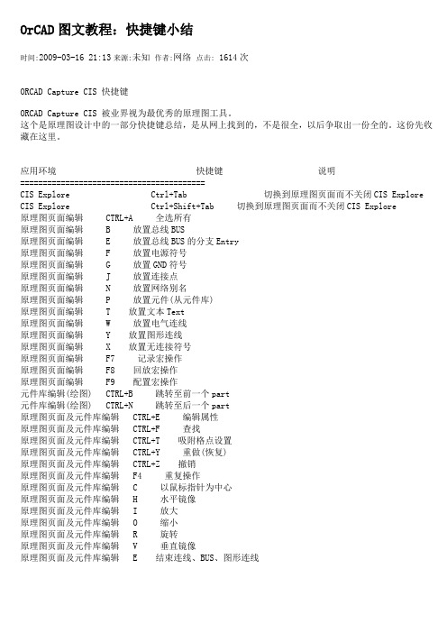
OrCAD图文教程:快捷键小结时间:2009-03-16 21:13来源:未知作者:网络点击:1614次ORCAD Capture CIS 快捷键ORCAD Capture CIS 被业界视为最优秀的原理图工具。
这个是原理图设计中的一部分快捷键总结,是从网上找到的,不是很全,以后争取出一份全的。
这份先收藏在这里。
应用环境快捷键说明=========================================CIS Explore Ctrl+Tab 切换到原理图页面而不关闭CIS ExploreCIS Explore Ctrl+Shift+Tab 切换到原理图页面而不关闭CIS Explore原理图页面编辑 CTRL+A 全选所有原理图页面编辑 B 放置总线BUS原理图页面编辑 E 放置总线BUS的分支Entry原理图页面编辑 F 放置电源符号原理图页面编辑 G 放置GND符号原理图页面编辑 J 放置连接点原理图页面编辑 N 放置网络别名原理图页面编辑 P 放置元件(从元件库)原理图页面编辑 T 放置文本Text原理图页面编辑 W 放置电气连线原理图页面编辑 Y 放置图形连线原理图页面编辑 X 放置无连接符号原理图页面编辑 F7 记录宏操作原理图页面编辑 F8 回放宏操作原理图页面编辑 F9 配置宏操作元件库编辑(绘图) CTRL+B 跳转至前一个part元件库编辑(绘图) CTRL+N 跳转至后一个part原理图页面及元件库编辑 CTRL+E 编辑属性原理图页面及元件库编辑 CTRL+F 查找原理图页面及元件库编辑 CTRL+T 吸附格点设置原理图页面及元件库编辑 CTRL+Y 重做(恢复)原理图页面及元件库编辑 CTRL+Z 撤销原理图页面及元件库编辑 F4 重复操作原理图页面及元件库编辑 C 以鼠标指针为中心原理图页面及元件库编辑 H 水平镜像原理图页面及元件库编辑 I 放大原理图页面及元件库编辑 O 缩小原理图页面及元件库编辑 R 旋转原理图页面及元件库编辑 V 垂直镜像原理图页面及元件库编辑 E 结束连线、BUS、图形连线orcad 是一个十分受欢迎的原理图设计软件,其他的功能我就不做过多评论了,但原理图设计工具确实很好用,著名的pcb软件cadence allegro SPB系列集成的原理图工具就是这个。
信号完整性揭秘:于博士SI设计手记

电源完整性是信号完整性的重要组成部分。本书最后介绍了电源完整性的基 础知识,包括电源分配网络的设计、电源噪声的来源和抑制方法等。这些知识将 帮助读者在解决电源问题时更加得心应手。
通过对于博士SI设计手记的深入剖析,我们可以看到,《信号完整性揭秘: 于博士SI设计手记》不仅提供了丰富的理论知识,还通过实例和设计指南帮助读 者更好地理解和应用这些知识。这本书无疑为电子工程领域的专业人员提供了一 本宝贵的参考书籍,无论是在学术研究还是在工程实践中,都将发挥重要的作用。 这本书也适合作为本科生和研究生的教材或参考书籍,帮助他们在学习过程中掌 握信号完整性的关键知识。
“信号完整性设计就像是侦探破案,我们需要收集线索,分析证据,然后找 出问题的真正原因。在这个过程中,我们需要有敏锐的观察力和扎实的专业知 识。”
“电子系统的设计是一个不断迭代和优化的过程。只有经过反复的实验和验 证,我们才能找到最佳的设计方案。”
这些摘录不仅展示了于博士对于信号完整性设计的深入理解,也为我们提供 了一种全新的视角来看待电子系统设计中的问题。这本书不仅适合电子设计工程 师阅读,也适合于对电子系统设计感兴趣的读者。通过这本书,我们可以更深入 地理解信号完整性的重要性以及如何解决信号完整性问题的过程。
本书接着探讨了信号完整性问题及其对系统性能的影响。反射、串扰、地弹 等问题是信号完整性的主要挑战。通过实例和理论分析,本书帮助读者理解这些 问题产生的原因和解决方法。还讨论了这些问题对系统性能的影响,包括可能导 致的数据错误和系统故障。
在高速串行互连设计中,需要了解许多复杂的知识,包括S参数、差分互连、 阻抗不连续性、抖动、均衡等。本书深入浅出地解释了这些复杂的概念,并提供 了实用的设计指南。还通过实例说明了这些知识在实际设计中的应用。
电源完整性测试
刘婷 婷 , 邓 豹, 韩 熳 莉
( 中航 工 业 西 安 航 空 计 算 技 术研 究所 , 陕西 西安 7 1 0 0 6 5 )
摘 要 : 随 着 电 子 产 品 小 型 化 以 及 复 杂 化 的 发 展 , 电 源 完 整 性 的 设 计 已 经 成 为 了 制 约 高速 电路 设 计 成 败 的 关 键 因 素 之 一 。 能 够 正 确 地 测 试 到 电 源 完 整 性 参 数 对 于 产 品 调 试 来 说 是 最 根 本 、 最 重 要
必 须 首 先 保 证 电 源 电 路 高 质 量 工 作 。 高 速 电 路 的 设 计
复 杂 性 使 得 电 源 完 整 性 的 测 试 工 作 也 变 得 很 困 难 。 电
尔时代 。 集 成 电 子器 件 的 规模 越 来 越 大 。 一个 芯 片 核 中
集 成几 十亿 只 晶体管 , 由 此 带 来 芯 片 的 时 钟 频 率 不 断 提 高, 供 电 电压 在 不 断降 低 , 相 应 的 功 率 和 电 流 量 级 显 著
t h e mo s t f u n d a me n t a l a n d mo s t i mp o r t a n t p a t r .I n o r d e r t o o b t a i n a c c u r a t e p o we r i n t e g r i t y t e s t p a r a me t e s,f r r o m t e s t e q u i p me n t a n d
s u p p l y, a n d p r o v i d e s a t e s t p r o c e d u r e .
非连续平面结构的电源完整性研究
面结构分割、 嵌入式电容集成[8]和表贴式去耦电容焊 接[9]等。 建立 PDN 等效电路, 是实现最优电容添加方案, 进而实现 PDN 网络低阻抗的先决条件。 2011 年,Jingook 等[10]建立了一种多层 PCB 通 孔结构中电源总线的等效电路模型,用于计算和分 析板级 PDN 连续结构的阻抗等电路参数。 2014 年,Zhao 等[11]建立了一种基于 mesh 网格 划分的单电源分布网络等效电路模型,用于提高大 电流密度的 TSV 三维连接结构芯片可靠性。 2017 年,
基金项目 :国家自然科学基金资助项目(61404119) 收稿日期: 2017-09-08 通讯作者 :尹学全 作者简介 :尹学全(1990-) ,男,内蒙古宁城人,研究生,主要研究方向为信号与信息处理。
72
尹学全等:非连续平面结构的电源完整性研究
Vol.37 No.1 Jan. 2018
Nayak 等[12]提出了一种基于非正交 2.5 维空间变换 和微单元分割的等效电路模型建立方法,用于分析 封装级的电源完整性。 但是,上述方法均没有建立封装级电源非连续 平面结构的等效电路模型,无法有效解决封装级多 电源分配网络的噪声隔离难题。对于多电源非连续 平面结构的等效电路模型以及建立模型应用于实际 产品鲜有报道。为此,本文针对电源非连续平面结 构建立了基于非正交三维空间变换的等效电路模 型,通过保角变换等共形映射的方法进行了分离单 元间互耦电容与互感的提取。基于本文提出的电路 模型与电路参数计算结果,设计了表贴式去耦电容 的拓扑方案。最后,采用 LTCC 技术和 SiP 封装技 术,成功研制出了一款集成多电源的多功能模块, 实测结果表明, 基于本文提出的方法所研制的模块, 其电源纹波小于 10 mV,噪声隔离性能优异。
电动汽车电机控制器的电源完整性分析
电动汽车电机控制器的电源完整性分析近年来,随着电子技术的发展,硬件电子系统变得越来越复杂,电源和地平面的噪声所带来的电源完整性(Power Integrity,PI)问题越来越突出,会影响到整个硬件系统的电磁兼容性(EMC)。
而谐振是电源完整性的一大问题,PCB 电源平面间谐振振幅过大,会导致电源分配网络(PDN)工作异常,甚至成为EMI辐射源,因此在PCB设计阶段需开展谐振仿真分析并消除谐振,这是提高设计成功率的一个有效方法。
为消除谐振,采用SIwave有限元仿真软件对电源地平面间的谐振情况进行仿真分析,找出谐振点,然后合理选用布局去耦电容,消除谐振影响。
标签:电动汽车;电机控制;电源;完整性1 引言本文采用了一种基于PI理论的硬件设计方法,构建了以NXP公司的32位单片机作为核心处理器的新能源汽车电机控制器系统。
在系统的PCB板设计前、后对PDN进行谐振仿真分析,并根据分析结果来优化设计,以确保系统稳定性和可靠性。
2 电机控制器的硬件架构和工作原理电机控制器是新能源电动汽车的核心部件之一,决定了汽车的动力性能。
它从整车控制器获得整车的需求,从动力电池包获得电能,经过自身逆变器的调制,获得控制电机需要的电流和电压,提供给电动机,使得电机的转速和转矩满足整车的要求。
本文设计的电机控制器以单片机MC56F8323为核心控制芯片,该系统的硬件构架如图1所示。
系统包括PWM波生成电路、复位电路、传感器信号处理电路、交互电路。
中央控制模块通过对外接口,得到整车上其他部件的指令和状态信息,同时把翻译过的指令传递给逆变器驱动电路,并检测控制效果。
3 电机控制器的电源完整性分析3.1 电源完整性及其影响因素电源完整性是指系统供电电源在经过一定的传输网络后在指定器件端口相对该器件对工作电源要求的符合程度。
虽然电源完整性是讨论电源供给的稳定性问题,但由于地在实际系统中总是和电源密不可分的,通常把如何减少地平面的噪声也作为电源完整性的一部分进行讨论。
继电保护用开关电源的故障分析及改进措施 于晶
继电保护用开关电源的故障分析及改进措施于晶摘要:继电保护开关电源和普通电源相比,其高效率、安全性、可靠性、抗干扰性都比较明显,还具有体积小、重量轻的优势,在恶劣天气下依旧能够可靠运行。
虽然继电保护用开关电源优势突出,但受各种因素的影响,无法避免故障的发生。
为了更好地发挥继电保护用开关电源的优势,针对故障危害,提出了有效的改进措施,以提升继电保护系统安全可靠性。
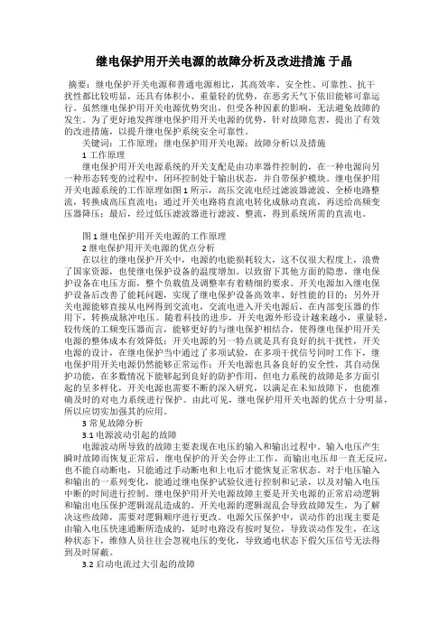
关键词:工作原理;继电保护用开关电源;故障分析以及措施1工作原理继电保护用开关电源系统的开关支配是由功率器件控制的,在一种电源向另一种形态转变的过程中,闭环控制处于输出状态,并自带保护模块。
继电保护用开关电源系统的工作原理如图 1 所示,高压交流电经过滤波器滤波、全桥电路整流,转换成高压直流电;通过开关电路将直流电转化成脉动直流,再送给高频变压器降压;最后,经过低压滤波器进行滤波、整流,得到系统所需的直流电。
图 1 继电保护用开关电源的工作原理2 继电保护用开关电源的优点分析在以往的继电保护开关中,电源的电能损耗较大,这不仅很大程度上,浪费了国家资源,也使继电保护设备的温度增加。
以致留下其他方面的隐患,继电保护设备在电压方面,整个负载值及调整率有着精细的要求。
开关电源加入继电保护设备后改善了能耗问题,实现了继电保护设备高效率、好性能的目的;另外开关电源能够直接从电网得到交流电,交流电进入开关电源后,在内部变压器的作用下,转换成脉冲电压。
随着科技的进步,开关电源外形设计越来越小,重量轻,较传统的工频变压器而言,能够更好的与继电保护相结合,使得继电保护用开关电源的整体成本有效降低;开关电源的另一特点就是具有良好的抗干扰性,开关电源的设计,在继电保护当中通过了多项试验,在多项干扰信号同时工作下,继电保护用开关电源仍然能够正常运作;开关电源也具备良好的安全性,其自动保护功能,在多数情况下能够起到良好的防护作用,但电力系统的故障是多方面引起的呈多样化,开关电源也需要不断的深入研究,以满足在未知故障下,也能准确及时的对电力系统进行保护。
60分钟学会OrCAD中文教程(SIG007版)
于博士信号完整性研究网60分钟学会OrCAD Capture CIS作者:于争 博士2009年4月28日目录1 建立工程及设置......................................................................................................................- 1 -2 工程管理器..............................................................................................................................- 4 -3 原理图页相关操作..................................................................................................................- 5 -4 创建元件库..............................................................................................................................- 6 -5 元件库编辑一些知识技巧......................................................................................................- 9 -6 如何创建不规则图形元件....................................................................................................- 10 -7 分裂元件................................................................................................................................- 15 -8 把一个元件分多个部分画出来............................................................................................- 16 -8.1 Homogeneous类型元件画法......................................................................................- 16 -8.2 Heterogeneous类型元件画法..................................................................................- 17 -8.3 分裂元件使用方法.....................................................................................................- 19 -9 加入元件库放置元件............................................................................................................- 21 -9.1普通元件放置方法......................................................................................................- 21 -9.2 电源和地的放置方法.................................................................................................- 23 -10 同一个页面内建立互连......................................................................................................- 24 -11 不同页面间建立互联的方法..............................................................................................- 26 -12 使用总线..............................................................................................................................- 27 -12.1 如何创建总线...........................................................................................................- 27 -12.2 放置非90度转角总线.............................................................................................- 28 -12.3 总线命名...................................................................................................................- 28 -12.4 总线与信号线连接...................................................................................................- 28 -13 浏览工程及使用技巧..........................................................................................................- 29 -13.1 浏览parts................................................................................................................- 30 -13.2 浏览nets..................................................................................................................- 31 -14 原理图中搜索......................................................................................................................- 32 -14.1 搜索元件...................................................................................................................- 33 -14.2 查找网络 flat nets...............................................................................................- 34 -15 元件替换与更新..................................................................................................................- 35 -15.1 批量替换 replace cache.......................................................................................- 35 -15.2 批量更新 update cache.........................................................................................- 36 -15.3 两个命令的区别.......................................................................................................- 36 -16 一些基本操作......................................................................................................................- 36 -16.1选择元件....................................................................................................................- 36 -16.2 移动元件...................................................................................................................- 37 -16.3 元件的旋转...............................................................................................................- 37 -16.4 元件的镜像翻转.......................................................................................................- 37 -16.5 修改元件属性放置文本...........................................................................................- 37 -17 添加footprint属性..............................................................................................................- 38 -17.1 单个元件添加Footprint属性...............................................................................- 38 -17.2 批量添加Footprint属性.......................................................................................- 41 -18 生成Netlist..........................................................................................................................- 44 -19 生成元件清单......................................................................................................................- 47 -20 打印原理图..........................................................................................................................- 51 -60分钟学会OrCAD Capture CIS1 建立工程及设置首先启动OrCAD Capture CIS选design entry CIS,如图。
华为公司是如何开展信号完整性与电源完整性分析研究工作的
华为公司是如何开展信号完整性与电源完整性分析研究工作的姜向中;厉进军;张胜利
【期刊名称】《中国集成电路》
【年(卷),期】2006(15)2
【摘要】@@ 华为公司互连设计部(早期的名称为CAD部)为了开发高速电路,随后为了解决电路电源稳定性问题,先后开展了信号完整性和电源稳定性的分析,研究工作;取得了一定成绩,在一定程度上,解决了产品开发中所遇到的问题,现将情况简介如下.
【总页数】2页(P81-82)
【作者】姜向中;厉进军;张胜利
【作者单位】无
【正文语种】中文
【中图分类】TN43
【相关文献】
1.华为专利检索与分析经验——访华为技术有限公司专利检索与分析组专业组组长李轶 [J], 王振瑜;姚琳
2.信号完整性与电源完整性的仿真分析与设计 [J], 李荔
3.信号完整性与电源完整性的仿真分析与设计 [J], 李荔
4.国网河南新多供电公司开展反窃电技术研究工作 [J], 张家轩;于红霞
5.三峡新能源公司与华为技术有限公司在山地光伏电站开展联合创新项目 [J],
因版权原因,仅展示原文概要,查看原文内容请购买。
- 1、下载文档前请自行甄别文档内容的完整性,平台不提供额外的编辑、内容补充、找答案等附加服务。
- 2、"仅部分预览"的文档,不可在线预览部分如存在完整性等问题,可反馈申请退款(可完整预览的文档不适用该条件!)。
- 3、如文档侵犯您的权益,请联系客服反馈,我们会尽快为您处理(人工客服工作时间:9:00-18:30)。
电源完整性设计作者:于博士一、为什么要重视电源噪声芯片内部有成千上万个晶体管,这些晶体管组成内部的门电路、组合逻辑、寄存器、计数器、延迟线、状态机、以及其他逻辑功能。
随着芯片的集成度越来越高,内部晶体管数量越来越大。
芯片的外部引脚数量有限,为每一个晶体管提供单独的供电引脚是不现实的。
芯片的外部电源引脚提供给内部晶体管一个公共的供电节点,因此内部晶体管状态的转换必然引起电源噪声在芯片内部的传递。
对内部各个晶体管的操作通常由内核时钟或片内外设时钟同步,但是由于内部延时的差别,各个晶体管的状态转换不可能是严格同步的,当某些晶体管已经完成了状态转换,另一些晶体管可能仍处于转换过程中。
芯片内部处于高电平的门电路会把电源噪声传递到其他门电路的输入部分。
如果接受电源噪声的门电路此时处于电平转换的不定态区域,那么电源噪声可能会被放大,并在门电路的输出端产生矩形脉冲干扰,进而引起电路的逻辑错误。
芯片外部电源引脚处的噪声通过内部门电路的传播,还可能会触发内部寄存器产生状态转换。
除了对芯片本身工作状态产生影响外,电源噪声还会对其他部分产生影响。
比如电源噪声会影响晶振、PLL、DLL的抖动特性,AD转换电路的转换精度等。
解释这些问题需要非常长的篇幅,本文不做进一步介绍,我会在后续文章中详细讲解。
由于最终产品工作温度的变化以及生产过程中产生的不一致性,如果是由于电源系统产生的问题,电路将非常难调试,因此最好在电路设计之初就遵循某种成熟的设计规则,使电源系统更加稳健。
二、电源系统噪声余量分析绝大多数芯片都会给出一个正常工作的电压范围,这个值通常是±5%。
例如:对于3.3V 电压,为满足芯片正常工作,供电电压在3.13V到3.47V之间,或3.3V±165mV。
对于1.2V 电压,为满足芯片正常工作,供电电压在1.14V到1.26V之间,或1.2V±60mV。
这些限制可以在芯片datasheet中的recommended operating conditions部分查到。
这些限制要考虑两个部分,第一是稳压芯片的直流输出误差,第二是电源噪声的峰值幅度。
老式的稳压芯片的输出电压精度通常是±2.5%,因此电源噪声的峰值幅度不应超过±2.5%。
当然随着芯片工艺的提高,现代的稳压芯片直流精度更高,可能会达到±1%以下,TI公司的开关电源芯片TPS54310精度可达±1%,线性稳压源AMS1117可达±0.2%。
但是要记住,达到这样的精度是有条件的,包括负载情况,工作温度等限制。
因此可靠的设计还是以±2.5%这个值更把握些。
如果你能确保所用的芯片安装到电路板上后能达到更高的稳压精度,那么你可以为你的这款设计单独进行噪声余量计算。
本文着重电源部分设计的原理说明,电源噪声余量将使用±2.5%这个值。
电源噪声余量计算非常简单,方法如下:比如芯片正常工作电压范围为3.13V到3.47V之间,稳压芯片标称输出3.3V。
安装到电路板上后,稳压芯片输出3.36V。
那么容许电压变化范围为3.47-3.36=0.11V=110mV。
稳压芯片输出精度±1%,即±3.363*1%=±33.6mV。
电源噪声余量为110-33.6=76.4mV。
计算很简单,但是要注意四个问题:第一,稳压芯片输出电压能精确的定在3.3V么?外围器件如电阻电容电感的参数也不是精确的,这对稳压芯片的输出电压有影响,所以这里用了3.36V这个值。
在安装到电路板上之前,你不可能预测到准确的输出电压值。
第二,工作环境是否符合稳压芯片手册上的推荐环境?器件老化后参数还会和芯片手册上的一致么?第三,负载情况怎样?这对稳压芯片的输出电压也有影响。
第四,电源噪声最终会影响到信号质量。
而信号上的噪声来源不仅仅是电源噪声,反射串扰等信号完整性问题也会在信号上叠加噪声,不能把所有噪声余量都分配给电源系统。
所以,在设计电源噪声余量的时候要留有余地。
另一个重要问题是:不同电压等级,对电源噪声余量要求不一样,按±2.5%计算的话,1.2V电压等级的噪声余量只有30mV。
这是一个很苛刻的限制,设计的时候要谨慎些。
模拟电路对电源的要求更高。
电源噪声影响时钟系统,可能会引起时序匹配问题。
因此必须重视电源噪声问题。
三、电源系统的噪声来源电源系统的噪声来源有三个方面:第一,稳压电源芯片本身的输出并不是恒定的,会有一定的波纹。
这是由稳压芯片自身决定的,一旦选好了稳压电源芯片,对这部分噪声我们只能接受,无法控制。
第二,稳压电源无法实时响应负载对于电流需求的快速变化。
稳压电源芯片通过感知其输出电压的变化,调整其输出电流,从而把输出电压调整回额定输出值。
多数常用的稳压源调整电压的时间在毫秒到微秒量级。
因此,对于负载电流变化频率在直流到几百KHz之间时,稳压源可以很好的做出调整,保持输出电压的稳定。
当负载瞬态电流变化频率超出这一范围时,稳压源的电压输出会出现跌落,从而产生电源噪声。
现在,微处理器的内核及外设的时钟频率已经超过了600兆赫兹,内部晶体管电平转换时间下降到800皮秒以下。
这要求电源分配系统必须在直流到1GHz范围内都能快速响应负载电流的变化,但现有稳压电源芯片不可能满足这一苛刻要求。
我们只能用其他方法补偿稳压源这一不足,这涉及到后面要讲的电源去耦。
第三,负载瞬态电流在电源路径阻抗和地路径阻抗上产生的压降。
PCB板上任何电气路径不可避免的会存在阻抗,不论是完整的电源平面还是电源引线。
对于多层板,通常提供一个完整的电源平面和地平面,稳压电源输出首先接入电源平面,供电电流流经电源平面,到达负载电源引脚。
地路径和电源路径类似,只不过电流路径变成了地平面。
完整平面的阻抗很低,但确实存在。
如果不使用平面而使用引线,那么路径上的阻抗会更高。
另外,引脚及焊盘本身也会有寄生电感存在,瞬态电流流经此路径必然产生压降,因此负载芯片电源引脚处的电压会随着瞬态电流的变化而波动,这就是阻抗产生的电源噪声。
在电源路径表现为负载芯片电源引脚处的电压轨道塌陷,在地路径表现为负载芯片地引脚处的电位和参考地电位不同(注意,这和地弹不同,地弹是指芯片内部参考地电位相对于板级参考地电位的跳变)。
四、电容退耦的两种解释采用电容退耦是解决电源噪声问题的主要方法。
这种方法对提高瞬态电流的响应速度,降低电源分配系统的阻抗都非常有效。
对于电容退耦,很多资料中都有涉及,但是阐述的角度不同。
有些是从局部电荷存储(即储能)的角度来说明,有些是从电源分配系统的阻抗的角度来说明,还有些资料的说明更为混乱,一会提储能,一会提阻抗,因此很多人在看资料的时候感到有些迷惑。
其实,这两种提法,本质上是相同的,只不过看待问题的视角不同而已。
为了让大家有个清楚的认识,本文分别介绍一下这两种解释。
4.1从储能的角度来说明电容退耦原理。
在制作电路板时,通常会在负载芯片周围放置很多电容,这些电容就起到电源退耦作用。
其原理可用图1说明。
图1去耦电路,方向如图所示。
此时电当负载电流不变时,其电流由稳压电源部分提供,即图中的I为0,电容两端存储相当数量的电荷,其电荷数量容两端电压与负载两端电压一致,电流Ic和电容量有关。
当负载瞬态电流发生变化时,由于负载芯片内部晶体管电平转换速度极快,必须在极短的时间内为负载芯片提供足够的电流。
但是稳压电源无法很快响应负载电流的变不会马上满足负载瞬态电流要求,因此负载芯片电压会降低。
但是由于电化,因此,电流I容电压与负载电压相同,因此电容两端存在电压变化。
对于电容来说电压变化必然产生电流,不再为0,为负载芯片提供电流。
根据电容等式:此时电容对负载放电,电流Ic(公式1)只要电容量C足够大,只需很小的电压变化,电容就可以提供足够大的电流,满足负载瞬态电流的要求。
这样就保证了负载芯片电压的变化在容许的范围内。
这里,相当于电容预先存储了一部分电能,在负载需要的时候释放出来,即电容是储能元件。
储能电容的存在使负载消耗的能量得到快速补充,因此保证了负载两端电压不至于有太大变化,此时电容担负的是局部电源的角色。
从储能的角度来理解电源退耦,非常直观易懂,但是对电路设计帮助不大。
从阻抗的角度理解电容退耦,能让我们设计电路时有章可循。
实际上,在决定电源分配系统的去耦电容量的时候,用的就是阻抗的概念。
4.2从阻抗的角度来理解退耦原理。
将图1中的负载芯片拿掉,如图2所示。
从AB两点向左看过去,稳压电源以及电容退耦系统一起,可以看成一个复合的电源系统。
这个电源系统的特点是:不论AB两点间负载瞬态电流如何变化,都能保证AB两点间的电压保持稳定,即AB两点间电压变化很小。
图片2电源部分我们可以用一个等效电源模型表示上面这个复合的电源系统,如图3图3等效电源对于这个电路可写出如下等式:(公式2)我们的最终设计目标是,不论AB两点间负载瞬态电流如何变化,都要保持AB两点间电压变化范围很小,根据公式2,这个要求等效于电源系统的阻抗Z要足够低。
在图2中,我们是通过去耦电容来达到这一要求的,因此从等效的角度出发,可以说去耦电容降低了电源系统的阻抗。
另一方面,从电路原理的角度来说,可得到同样结论。
电容对于交流信号呈现低阻抗特性,因此加入电容,实际上也确实降低了电源系统的交流阻抗。
从阻抗的角度理解电容退耦,可以给我们设计电源分配系统带来极大的方便。
实际上,电源分配系统设计的最根本的原则就是使阻抗最小。
最有效的设计方法就是在这个原则指导下产生的。
五、实际电容的特性正确使用电容进行电源退耦,必须了解实际电容的频率特性。
理想电容器在实际中是不存在的,这就是为什么经常听到“电容不仅仅是电容”的原因。
实际的电容器总会存在一些寄生参数,这些寄生参数在低频时表现不明显,但是高频情况下,其重要性可能会超过容值本身。
图4是实际电容器的SPICE模型,图中,ESR代表等效串联电阻,ESL代表等效串联电感或寄生电感,C为理想电容。
图4电容模型等效串联电感(寄生电感)无法消除,只要存在引线,就会有寄生电感。
这从磁场能量变化的角度可以很容易理解,电流发生变化时,磁场能量发生变化,但是不可能发生能量跃变,表现出电感特性。
寄生电感会延缓电容电流的变化,电感越大,电容充放电阻抗就越大,反应时间就越长。
等效串联电阻也不可消除的,很简单,因为制作电容的材料不是超导体。
讨论实际电容特性之前,首先介绍谐振的概念。
对于图4的电容模型,其复阻抗为:(公式3)当频率很低时,远小于,整个电容器表现为电容性,当频率很高时,大于,电容器此时表现为电感性,因此“高频时电容不再是电容”,而呈现为电感。
当时,,此时容性阻抗矢量与感性阻抗之差为0,电容的总阻抗最小,表现为纯电阻特性。