霍尔传感器ES249中文手册
霍尔传感器IC分类

-
Q & A ( 3)
Q:ES2481与ES2482的区别? A:对于最新出的ES2481和ES2482两个产品,虽然名称相近,但是功能 却大不相同。 ES2481是一个单输出的产品,它可以分为ES2481H和ES2481L。 ES2481H在无磁场时输出为高,ES2481L无磁场时输出为低。 ES2482是一个双输出的产品,能同时检测N、S极,它的这一特性可以很 好的应用于玩具当中。
按输出分类(7)
微功耗霍尔IC
• 优化功耗设计的霍尔IC
风扇马达驱动霍尔IC
• 专为直流风扇设计的霍尔IC
齿轮霍尔IC
• 专为齿轮设计的霍尔IC
-
Q & A ( 1)
Q:ES495与ES49E有什么区别? A:ES495的输出是rail-to-rail输出,即霍尔IC的输出电压最高可以接近正 电源电压,最低可以低至负电源电压,该特性使得ES495的电压范围比较 广,可调空间大,被广泛应用于工业领域。 ES49E电路简单、应用普遍,大量应用与电动车调速把上。
易盛课堂
——霍尔传感器IC分类
2014.2.20
-
课题讨论安排
按工艺分类
Q&A
按输出分类
-
按工艺分类(1)
CMOS工艺
易良盛科技霍尔传感器IC可以分为:
Bipolar工艺
CMOS工艺
• 霍尔IC器件内部集成了上百个甚至上千个场效应管
A:霍尔传感器常常指一个比较大一点的模块,霍尔IC或霍尔元件只是
它其中的一部分; 霍尔元件只是根据霍尔效应集成的一个敏感元件,是复合材料; 霍尔IC是Si制作,集成了霍尔敏感元件和少量简单处理的电路。
-
A44E霍尔传感器资料
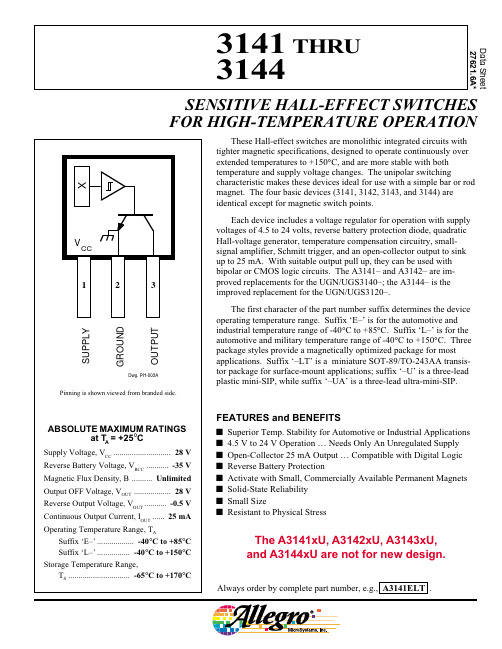
Data Sheet 27621.6A*Always order by complete part number, e.g., A3141ELT .These Hall-effect switches are monolithic integrated circuits with tighter magnetic specifications, designed to operate continuously over extended temperatures to +150°C, and are more stable with both temperature and supply voltage changes. The unipolar switchingcharacteristic makes these devices ideal for use with a simple bar or rod magnet. The four basic devices (3141, 3142, 3143, and 3144) are identical except for magnetic switch points.Each device includes a voltage regulator for operation with supply voltages of 4.5 to 24 volts, reverse battery protection diode, quadratic Hall-voltage generator, temperature compensation circuitry, small-signal amplifier, Schmitt trigger, and an open-collector output to sink up to 25 mA. With suitable output pull up, they can be used with bipolar or CMOS logic circuits. The A3141– and A3142– are im-proved replacements for the UGN/UGS3140–; the A3144– is the improved replacement for the UGN/UGS3120–.The first character of the part number suffix determines the deviceoperating temperature range. Suffix ‘E–’ is for the automotive and industrial temperature range of -40°C to +85°C. Suffix ‘L–’ is for the automotive and military temperature range of -40°C to +150°C. Three package styles provide a magnetically optimized package for most applications. Suffix ‘–LT’ is a miniature SOT-89/TO-243AA transis-tor package for surface-mount applications; suffix ‘–U’ is a three-lead plastic mini-SIP, while suffix ‘–UA’ is a three-lead ultra-mini-SIP.FEATURES and BENEFITSs Superior Temp. Stability for Automotive or Industrial Applications s 4.5 V to 24 V Operation … Needs Only An Unregulated Supply s Open-Collector 25 mA Output … Compatible with Digital Logic s Reverse Battery Protections Activate with Small, Commercially Available Permanent Magnets s Solid-State Reliability s Small Sizes Resistant to Physical StressSENSITIVE HALL-EFFECT SWITCHES FOR HIGH-TEMPERATURE OPERATION3141 THRU 3144The A3141xU, A3142xU, A3143xU,and A3144xU are not for new design.3141 THRU 3144SENSITIVEHALL-EFFECT SWITCHESFOR HIGH-TEMP. OPERATION115 Northeast Cutoff, Box 15036Worcester, Massachusetts 01615-0036 (508) 853-5000MAGNETIC CHARACTERISTICS in gauss over operating supply voltage range.NOTES:Typical values are at T A = +25°C and V CC = 8 V.B OP = operate point (output turns ON); B RP = release point (output turns OFF); B hys = hysteresis (B OP - B RP ).*Complete part number includes a suffix to identify operating temperature range (E- or L-) and package type ( -LT, -U, or -UA).ELECTRICAL CHARACTERISTICS at V CC = 8 V over operating temperature range.LimitsCharacteristic Symbol Test ConditionsMin.Typ.Max.Units Supply VoltageV CC Operating 4.524V Output Saturation Voltage V OUT(SAT)I OUT = 20 mA, B > B OP 175400mV Output Leakage Current I OFF V OUT = 24 V, B < B RP <1.010µA Supply Current I CC B < B RP (Output OFF) 4.49.0mA Output Rise Time t r R L = 820 Ω, C L = 20 pF 0.04 2.0µs Output Fall Timet fR L = 820 Ω, C L = 20 pF0.18 2.0µsPart Numbers*A3141–A3142– A3143–A3144–Characteristic Min.Typ.Max.Min.Typ.Max.Min.Typ.Max.Min.Typ.Max.B OP at T A = 25°C5010016013018023022028034070350over operating temp. range 3010017511518024520528035535450B RP at T A = 25°C10451307512517516522528550330over operating temp. range 10451456012519015022530025430B hys at T A = 25°C2055803055803055802055over operating temp. range2055803055803055802055Copyright © 1993, 1999, Allegro MicroSystems, Inc.3141 THRU 3144SENSITIVEHALL-EFFECT SWITCHES FOR HIGH-TEMP . OPERATIONSUPPLY CURRENTSUPPLY CURRENT10152025SUPPLY VOLTAGE IN VOLTSDwg. GH-041-15S U P P L Y C U R R E N T I N m A255075AMBIENT TEMPERATURE IN °C-50Dwg. GH-039-1-25S U P P L Y C U R R E N T I N m ATYPICAL OPERATING CHARACTERISTICSA3142– SWITCH POINTSOUTPUT SATURATION VOLTAGE300AMBIENT TEMPERATURE IN °C200Dwg. GH-040-1S A T U R A T I O N V O L T A G E I N m V50100AMBIENT TEMPERATURE IN °C-50Dwg. GH-044S W I T C H P O I N T I N G A U S S3004002001001500-252575125* Complete part number includes a suffix denoting operating temperature range (E- or L-) and package type ( -LT, -U, or -UA).3141 THRU 3144SENSITIVEHALL-EFFECT SWITCHESFOR HIGH-TEMP. OPERATION115 Northeast Cutoff, Box 15036Worcester, Massachusetts 01615-0036 (508) 853-5000TYPICAL OPERATING CHARACTERISTICS (cont.)CHANGE IN OPERATE POINT10152025SUPPLY VOLTAGE IN VOLTSDwg. GH-042-15C H A N G E I N O P E R A T E P O I N T I N G A U S S-5.05.0OPERATIONThe output of these devices (pin 3) switches low when the magnetic field at the Hall sensor exceeds the operate point threshold (B OP ). At this point, the output voltage is V OUT(SAT). When the magnetic field is reduced to below the release point threshold (B RP ), the device output goes high. The difference in the magnetic operate and release points is called the hysteresis (B hys ) of the device. This built-in hysteresis allows clean switching of the output even in the presence of external mechanical vibration and electrical noise.3141 THRU 3144SENSITIVE HALL-EFFECT SWITCHES FOR HIGH-TEMP. OPERATION PACKAGE DESIGNATOR ‘LT’(SOT-89/TO-243AA)Dimensions in Inches(for reference only)Dimensions in Millimeters(controlling dimensions)0.440.35NOTES:1.Tolerances on package height and width represent allowable mold offsets. Dimensions given are measured at the widest point (parting line).2.Exact body and lead configuration at vendor’s option within limits shown.3.Height does not include mold gate flash.3141 THRU 3144SENSITIVEHALL-EFFECT SWITCHESFOR HIGH-TEMP. OPERATION115 Northeast Cutoff, Box 15036Worcester, Massachusetts 01615-0036 (508) 853-5000°°NOTES:1.Tolerances on package height and width represent allowable mold offsets. Dimensions given are measuredat the widest point (parting line).2.Exact body and lead configuration at vendor’s option within limits shown.3.Height does not include mold gate flash.4.Recommended minimum PWB hole diameter to clear transition area is 0.035" (0.89 mm).PACKAGE DESIGNATOR ‘U’Dimensions in Inches Dimensions in Millimeters (controlling dimensions)(for reference only)Devices in the ‘U’ package areNOT RECOMMENDED FOR NEW DESIGN3141 THRU 3144SENSITIVE HALL-EFFECT SWITCHES FOR HIGH-TEMP. OPERATION Dwg. MH-014E inBSC°NOTES:1.Tolerances on package height and width represent allowable mold offsets. Dimensions given are measured at the widest point (parting line).2.Exact body and lead configuration at vendor’s option within limits shown.3.Height does not include mold gate flash.Dwg. MH-014E mmBSC °PACKAGE DESIGNATOR ‘UA’Dimensions in Inches Dimensions in Millimeters (controlling dimensions)(for reference only)3141 THRU 3144SENSITIVEHALL-EFFECT SWITCHESFOR HIGH-TEMP. OPERATION115 Northeast Cutoff, Box 15036Worcester, Massachusetts 01615-0036 (508) 853-5000Allegro MicroSystems, Inc. reserves the right to make, from time to time,such departures from the detail specifications as may be required to permit improvements in the design of its products.The information included herein is believed to be accurate and reliable.However, Allegro MicroSystems, Inc. assumes no responsibility for its use;nor for any infringements of patents or other rights of third parties which may result from its use.。
霍尔传感器中文手册

1.描述ES582是单极霍尔效应传感器从混合信号IC制造CMOS技术。
设备集成了一个电压调节器,霍尔传感器动态补偿取消系统,施密特触发器和一个open-drain输出驱动程序,所有在一个包中。
它集成了先进的直升机稳定技术提供准确和稳定的磁开关点。
有很多申请这HED -霍尔电子设备除了那些下面列出。
由于其宽工作电压范围和扩展温度范围的选择,它非常适用于汽车,工业和消费者应用程序。
交付的设备是在一个小提纲晶体管(说)表面安装过程和在一个塑料单(- 92平)通孔。
3-lead 包都是通过无铅认证。
2.特性宽工作电压范围3.5 v和24 v介质的敏感性CMOS技术Chopper-stabilized放大级优良的温度稳定性极低的开关点漂移对身体压力低电流消耗明渠输出小SOT23 3 l和平板- 92 3 l,通过无铅认证包3.应用程序汽车、消费品和工业固态开关断续器速度检测线性位置检测角位置检测接近detectio4.原理框图5.术语表术语描述毫伏特斯拉(mT) 高斯,磁通密度单位:1吨= 10高斯 RoHS有害物质限制SOT 小轮廓晶体管(说包)——也被称为包代码” ESD 静电放电 BLDCBrush-Less 直流操作点(BOP)磁通密度应用于品牌的包将输出驱动程序(输出电压= VDSon)释放点(BRP)磁通密度应用于品牌的包挫伤了驱动程序的输出(输出电压=高)6.销的定义和描述SE 销UA 销.类型函数名称 1 1 V DD 输入 电源电压销 2 3 OUT 输出 输出销 32GND接地地面销VDDOUTV oltage Regulat o rChopperHall PlateGNDUA Package SO Package Pin 1 – V DDPin 1 – V DDPin 2 – GND P in 2 – OUT Pin 3 – OUT P in 3 – GND7.独特的特性基于混合信号CMOS技术,Innosen ES582霍尔设备与介质磁敏感性。
霍尔传感器用法
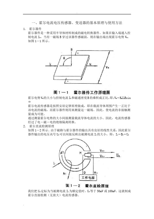
一、霍尔电流电压传感器、变送器的基本原理与使用方法1.霍尔器件霍尔器件是一种采用半导体材料制成的磁电转换器件。
如果在输入端通入控制电流IC ,当有一磁场B穿过该器件感磁面,则在输出端出现霍尔电势VH。
如图1-1所示。
霍尔电势VH 的大小与控制电流IC和磁通密度B的乘积成正比,即:VH=KHICBsinΘ霍尔电流传感器是按照安培定律原理做成,即在载流导体周围产生一正比于该电流的磁场,而霍尔器件则用来测量这一磁场。
因此,使电流的非接触测量成为可能。
通过测量霍尔电势的大小间接测量载流导体电流的大小。
因此,电流传感器经过了电-磁-电的绝缘隔离转换。
2.霍尔直流检测原理如图1-2所示。
由于磁路与霍尔器件的输出具有良好的线性关系,因此霍尔器件输出的电压讯号U0可以间接反映出被测电流I1的大小,即:I1∝B1∝U我们把U0定标为当被测电流I1为额定值时,U等于50mV或100mV。
这就制成霍尔直接检测(无放大)电流传感器。
3.霍尔磁补偿原理原边主回路有一被测电流I1,将产生磁通Φ1,被副边补偿线圈通过的电流I2所产生的磁通Φ2进行补偿后保持磁平衡状态,霍尔器件则始终处于检测零磁通的作用。
所以称为霍尔磁补偿电流传感器。
这种先进的原理模式优于直检原理模式,突出的优点是响应时间快和测量精度高,特别适用于弱小电流的检测。
霍尔磁补偿原理如图1-3所示。
从图1-3知道:Φ1=Φ2I1N1=I2N2I2=NI/N2·I1当补偿电流I2流过测量电阻RM时,在RM两端转换成电压。
做为传感器测量电压U0即:U=I2RM按照霍尔磁补偿原理制成了额定输入从0.01A~500A系列规格的电流传感器。
由于磁补偿式电流传感器必须在磁环上绕成千上万匝的补偿线圈,因而成本增加;其次,工作电流消耗也相应增加;但它却具有直检式不可比拟的较高精度和快速响应等优点。
4.磁补偿式电压传感器为了测量mA级的小电流,根据Φ1=I1N1,增加N1的匝数,同样可以获得高磁通Φ1。
常闭型全极霍尔YS2481中文产品手册

YS2481
注意事项
1.霍尔是敏感器件,在使用过程以及存储过程中请注意采取静电防护措施。
2.霍尔在安装过程中应尽量避免对霍尔本体施加机械应力,如管脚需要弯曲请在距引线根部3MM 以外操作。
3.建议焊接温度:电烙铁焊接,建议温度350℃,最长5秒。
波峰焊:建议最高温度260℃,最长3秒红外回流焊:建议最高245℃,最长10秒
4.不建议超越数据表中的参数使用,虽然极限参数下霍尔会正常工作,但是长时间处于极限条件下可能会造成霍尔或者实际产品的损坏,为了保障霍尔的正常工作和产品的安全性稳定性,请在数据表许可范围内使用。
YAV 霍尔电流传感器 技术手册v1708

霍尔电流传感器
工作 环境
环境温度
-25℃~+80℃
贮存温度
相对湿度
≤90%
气压条件
AC/DC ±10A ±1ຫໍສະໝຸດ 0A ±100A额定电流范围
误差非线性
可选
输出
0-5V/10V/20mA 可选
测量电流范围
过载倍数
无限
工作频率
电气 参数
工作电源 绝缘阻抗
±12V ±24+5%V
功耗 绝缘耐压
-40℃~+115℃ 正常大气压 0.1% 量程标注 0-10khz +18, -10ma 5kV50hz1Min)
1. 产品概述
YAV 直流/交流电流传感器是一种检测装置,能感受到被测电流的信息,并能将检测感受到的信息,按 一定规律变换成为符合一定标准需要的电信号或其他所需形式的信息输出,以满足信息的传输、处理、存 储、显示、记录和控制等要求。
电流变送器是一种利用磁通门原理将被测直流电流转换成与该电流成比例输出的直流电流或电压信号 的测量模块,原副边之间高度绝缘。具有高精确度、高线性度、高集成度、体积小结构简单、长期工作稳 定且适应各种工作环境的特点。广泛地应用在新能源、石油、煤矿、化工、铁路、通信、楼宇自控等行业 的电气设备的系统控制及检测。
直流微电流测量的电量隔离传感器,测量方式为穿孔结构,无插入损耗,过载能力强,抗电磁干扰能 力强,电源适应范围宽,其输入和输出之间都不共地,输入信号为直流微电流,可以用于测量直流系统绝 缘漏电流,该产品可广泛用于直流电源系统各回路的绝缘监测。
直流漏电流传感器是一种依据互感器电磁隔离、磁调制工作原理将被测直流微电流转换成直流电流、
II
武汉亚为电子科技有限公司
全极低功耗霍尔开关SS249使用手册

PackagesFeatures and Benefits3 pin SOT23 (suffix SO) 3 pin SIP (suffix UA)–Solid-State Reliability much better than reed Switch – Omnipolar, output switches with absolute value of North or South pole from magnet – Operation from 3.5V to 24V–High sensitivity for direct reed switch replacement applicationsFunctional Block Diagram Application Examples– Solid state switch – Speed detection – Interrupter–Magnet proximity sensor for reed switch replacementGeneral Description:The SS249 Omnipolar Hall effect sensor IC is fabricated from mixed signal CMOS technology .It incorporates advanced chopper-stabilization techniques to provide accurate and stable magnetic switch points.The output transistor of the SS249 will be latched on (BOP) in the presence of a sufficiently strong South or North magnetic field facing the marked side of the package. The output will be latched off (BRP) in the absence of a magnetic field.Typical Application CircuitSEC's pole-independent sensing technique allows for operation with either a north pole or south pole magnet orientation, enhancing the manufacturability of the device. The state-of-the-art technology provides the same output polarity for either pole face.It is strongly recommended that an external bypass be connected (in close proximity to the Hall sensor) between the supply and ground of the device to reduce both external noise and noise generated by the chopper-stabilization technique. This is especially true due to the relatively high impedance of battery supplies.Internal Timing CircuitAutomotive and Severe Environment Protection Circuit Typical Three-Wire Application CircuitPin Definitions and DescriptionsTable 1: Pin definitions and descriptionsAbsolute Maximum RatingsExceeding the absolute maximum ratings may cause permanent damage. Exposure to absolute-maximum-rated conditions for extended periods may affect device reliability.DC Electrical CharacteristicsDC Operating Parameters: T A = 25℃, V DD= 2.75V.Parameter Symbol Test Conditions Min Typ Max UnitsOperating Voltage V DD Operating 2.5 3 5.5 VSupply Current I DD Average 5 µAOutput Current I OUT 1.0 mASaturation Voltage V SAT I OUT = 1mA 0.4 VAwake mode time T AW Operating 175 µSSleep mode time T SL Operating 70 mSTable 3: DC electrical characteristicsMagnetic CharacteristicsOperating Parameters: T A = 25°C, V DD = 2.75V DCESD ProtectionPerformance CharacteristicsUnique FeaturesCMOS Hall IC TechnologyThe chopper stabilized amplifier uses switched capacitor techniques to eliminate the amplifier offset voltage, which, in bipolar devices, is a major source of temperature sensitive drift. CMOS makes this advanced technique possible. The CMOS chip is also much smaller than a bipolar chip, allowing very sophisticated circuitry to be placed in less space. The small chip size also contributes to lower physical stress and less power consumption.Installation CommentsConsider temperature coefficients of Hall IC and magnetic, as well as air gap and life time variations. Observe temperature limits during wave soldering. Typical IR solder-reflow profile:– No Rapid Heating and Cooling.– Recommended Preheating for max. 2minutes at 150°C– Recommended Reflowing for max. 5seconds at 240°CESD PrecautionsElectronic semiconductor products are sensitive to Electro Static Discharge (ESD).Always observe Electro Static Discharge control procedures whenever handling semiconductor products.Package UA, 3-Pin SIP:Package SOT, 3-Pin SOT-23:SOT-23 Package Hall Location:Ordering InformationPart No. Pb-free Temperature Code Package Code PackingSS249ESOT YES -40°C to 85°C SOT-23 7-in. reel, 3000 pieces/reel SS249EUA YES -40°C to 85°C TO-92 Bulk, 1000 pieces/bagSS249KSOT YES -40°C to 125°C SOT-23 7-in. reel, 3000 pieces/reel SS249KUA YES -40°C to 125°C TO-92 Bulk, 1000 pieces/bagSS249LSOT YES -40°C to 150°C SOT-23 7-in. reel, 3000 pieces/reel SS249LUA YES -40°C to 150°C TO-92 Bulk, 1000 pieces/bag。
常用传感器霍尔传感器的用法3144A44E
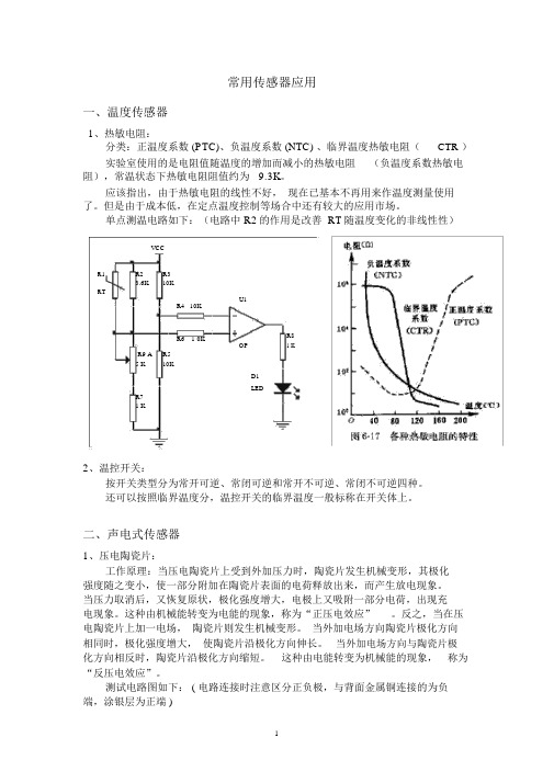
常用传感器应用一、温度传感器1、热敏电阻:分类:正温度系数 (PTC)、负温度系数 (NTC) 、临界温度热敏电阻(CTR )实验室使用的是电阻值随温度的增加而减小的热敏电阻(负温度系数热敏电阻),常温状态下热敏电阻阻值约为9.3K。
应该指出,由于热敏电阻的线性不好,现在已基本不再用来作温度测量使用了。
但是由于成本低,在定点温度控制等场合中还有较大的应用市场。
单点测温电路如下:(电路中 R2的作用是改善 RT随温度变化的非线性性)VCCR1R2R33.6K10KRTU1R4 10KR6 1 0K R81 KOPR9 A R55 K10KD1LEDR71 K2、温控开关:按开关类型分为常开可逆、常闭可逆和常开不可逆、常闭不可逆四种。
还可以按照临界温度分,温控开关的临界温度一般标称在开关体上。
二、声电式传感器1、压电陶瓷片:工作原理:当压电陶瓷片上受到外加压力时,陶瓷片发生机械变形,其极化强度随之变小,使一部分附加在陶瓷片表面的电荷释放出来,而产生放电现象。
当压力取消后,又恢复原状,极化强度增大,电极上又吸附一部分电荷,出现充电现象。
这种由机械能转变为电能的现象,称为“正压电效应”。
反之,当在压电陶瓷片上加一电场,陶瓷片则发生机械变形。
当外加电场方向陶瓷片极化方向相同时,极化强度增大,使陶瓷片沿极化方向伸长。
当外加电场方向与陶瓷片极化方向相反时,陶瓷片沿极化方向缩短。
这种由电能转变为机械能的现象,称为“反压电效应”。
测试电路图如下: ( 电路连接时注意区分正负极,与背面金属铜连接的为负端,涂银层为正端 )+5VR1 AR3R4R5R66 80350K13K 2.7 K500 KC1C2R2OUT1 K10u F 4 7u FQ1Q2Q3901 39013901 3Y12、驻极体话筒:驻极体话筒及其电路的接法有两种:源极输出与漏极输出。
源极输出类似晶体三极管的射极输出。
需用三根引出线。
漏极 D 接电源正极。
- 1、下载文档前请自行甄别文档内容的完整性,平台不提供额外的编辑、内容补充、找答案等附加服务。
- 2、"仅部分预览"的文档,不可在线预览部分如存在完整性等问题,可反馈申请退款(可完整预览的文档不适用该条件!)。
- 3、如文档侵犯您的权益,请联系客服反馈,我们会尽快为您处理(人工客服工作时间:9:00-18:30)。
6. Absolute Maximum Ratings
Parameter
Supply Voltage(operating) Supply Current
©2009-2013 Innosen Technology Co., Ltd.
Symbol
VDD IDD
Value
5.5 70
Units
V μA
2/5
Symbol
VDD IDD IOUT VSAT TAW TSL
Test Conditions
Operating Average
Min
2.5
Typ
3 45 1.0
Max
5.5
Units
V μA mA
IOUT=1mA Operating Operating 20
0.4
V μS μS
600
8.
Magnetic Characteristics
24921
3 - 0.44 3.90 0.05 0.05 3.90 3 - 0.39 3.90
Active Area Depth:
3 1
0.84(Nom) 6 1
2.3. 0.1
1 2
2 1
3 4
3 1
6 1
0.5 14
Notes: 1). Controlling dimension: mm; 2). Leads must be free of flash and plating voids; 3). Do not bend leads within 1 mm of lead to package interface; 4). PINOUT: Pin 1 Pin 2 Pin 3 VDD GND Output
©2009-2013 Innosen Technology Co., Ltd. Rev3.0.0.130116
FAX: 022-59812096
5/5
Top View
3
Notes: 1). PINOUT:
249mm
1
1.70 2.10
1.60 2.65 1.70 2.95
Pin 1 VDD Pin 2 Output Pin 3 GND 2). All dimensions are in millimeters; Marking: 249-- Code of Device ( ES249 ); y -- last 1 digit of year ; mm -- Production Lot ;
2. Features
CMOS Hall IC Technology Unipolar Output Solid-State Reliability much better than reed switch Operation down to 2.5V CMOS inverter output (no pull-up resistance) High sensitivity for direct reed switch replacement applications
9.2 TO-92 Package Physical Characteristics
0.76 0.05 1.58 0.1
ES249
2.13 1.87 3 1 45 1 1.00 1.20
4.1 0.1 3.90
1 2
2 1
3 4
Sensor Location
3.18 0.1
3
0.95 0.80 3.00 2 3 1 2 1.50 1.40
0.36 0.46
©2009-2013 Innosen Technology Co., Ltd.
Rev3.0.0.130116
4/5
Datasheet
Micropower High Sensitivity Hall Switch
Operating Parameters: TA = 25℃, VDD=3VDC Parameter
Operating Point Release Point Hysteresis
Symbol
BOP BRP BHYS
Min
Type
150
Max
200
Units
Gs Gs
50 -
90 60 -
Gs
©2009-2013 Innosen Technology Co., Ltd.
ES249
This serves to place the high current-consuming portions of the circuit into a “Sleep” mode. Periodically the device is “Awakened” by this internal logic and the magnetic flux from the Hall element is evaluated against the predefined thresholds. If the flux density is above or below the BOP/BRP thresholds then the output transistor is driven to change states accordingly. While in the “Sleep” cycle the output transistor is latched in its previous state. The design has been optimized for service in applications requiring extended operating lifetime in battery powered systems. The output transistor of the ES249 switches low (turns on) when the south pole magnetic field perpendicular to the Hall sensor exceeds the operate point threshold (B OP). After turn-on, the output voltage is VDS. When the magnetic field is reduced below the release point, BRP, the Output transistor turns off (goes high). The difference in the magnetic operate and release points is the hysteresis (BHYS) of the device. This built-in hysteresis prevents output oscillation near the switching point, and allows clean switching of the output even in the presence of external mechanical vibration and electrical noise. The TSOT-23 device is reversed from the UA package.
7. DC Electrical Characteristics
DC Operating Parameters: TA = 25℃, VDD=3V Parameter
Operating voltage Supply current Output Current Saturation Voltage Awake mode time Sleep mode time
Datasheet
Micropower High Sensitivity Hall Switch 1. Description
The ES249 Hall effect sensor IC is fabricated from mixed signal CMOS technology. It incorporates advanced chopper-stabilization techniques to provide accurate and stable magnetic switch points. The circuit design provides an internally controlled clocking mechanism to cycle power to the Hall element and analog signal processing circuits.
1.27
10. Ordering Information
Part No.
ES249
Package Code
UA (TO-92S) SO (SOT-23)
Contact Information:
Innosen Technology Co., Ltd. TEL: 022-59812098 WEB:
ES249
Magnet proximity sensor for reed switch replacement in low duty cycle applications
4. Functional Block Diagram
5. Internal Timing Circuit
Current Period Iaw Sample & Output Latched Iav Isp Awake Taw: 20cc 0 Sleep Tsl: 600μs Time
Rev3.0.0.130116
Datasheet
Micropower High Sensitivity Hall Switch