应用于MIPS内核的OCTEON家族处理器介绍
关于各代迅驰的知识

关于各代迅驰的知识2008年03月16日星期日 02:142003年3月英特尔正式发布了迅驰移动计算技术,英特尔的迅驰移动计算技术并非以往的处理器、芯片组等单一产品形式,其代表了一整套移动计算解决方案,迅驰的构成分为三个部分:奔腾M处理器、855/915系列芯片组和英特尔PRO无线网上,三项缺一不可共同组成了迅驰移动计算技术。
1、迅驰一代(Centrino)Pentium M处理器(Banis核心,单核,130nm制程, 1M二级缓存, 400FSB)+ 855芯片组(Intel 855GM/855PM)+ 802.11b无线网卡(Intel Pro/Wireless 2100)奔腾M处理器LOGO第一代迅驰logo奔腾M首次改版叫Dothan在两年多时间里,迅驰技术经历了一次改版和一次换代。
初期迅驰中奔腾M处理器的核心代号为Bannis,采用130纳米工艺,1MB高速二级缓存,400MHz前端总线。
迅驰首次改版是在2004年5月,采用90纳米工艺Dothan核心的奔腾M处理器出现,其二级缓存容量提供到2MB,前端总线仍为400MHz,它也就是我们常说的Dothan迅驰。
首次改版后,Dothan核心的奔腾M处理器迅速占领市场,Bannis核心产品逐渐退出主流。
虽然市场中流行着将Dothan核心称之为迅驰二代,但英特尔官方并没有给出明确的定义,仍然叫做迅驰。
也就是在Dothan奔腾M推出的同时,英特尔更改了以主频定义处理器编号的惯例,取而代之的是一系列数字,例如:奔腾M 715/725等,它们分别对应1.5GHz和1.6GHz主频。
首次改版中,原802.11b无线网卡也改为了支持802.11b/g规范,网络传输从11Mbps提供至14Mbps.新一代迅驰Sonoma也叫迅驰二代(Sonoma)Pentium M处理器(Dothan核心,单核,90nm制程, 2M二级缓存, 533FSB)+ 915芯片组(Intel 915GM/915PM)+ 802.11b/g无线网卡(Intel Pro/Wireless 2200GB/2915ABG)注:Intel Pro/Wireless 2915ABG支持802.11a/b/g协议。
力拼ARM全家 MIPS新品Aptiv处理器全解析

力拼ARM全家MIPS新品Aptiv处理器全解析5月10日晚间RISC处理器授权厂商MIPS正式发布了新一代产品Aptiv系列,包括ProAptiv、interAptiv和microAptiv三款,着力抗衡竞争对手ARM的整条产品线。
著名硬件网站Anandtech在第一时间拿到了MIPS提供的第一手资料,本文即为Anandtech分析介绍原文的多数内容编译版。
智能手机和平板电脑兴起之后,英国厂商ARM凭借多种处理器和图形核心IP授权占据了这块市场的绝大多数份额。
但ARM也不是一直在场独角戏,和该公司差不多同龄的MIPS同样做的是RISC处理器的授权业务。
之前MIPS凭借向Broadcom(博通)和Sigma Designs等授权已经将手伸向了家用娱乐/机顶盒等网络领域。
随着ARM的兴起,MIPS也逐渐在向迅速增长的移动/平板领域扩张。
当地时间5月10日,MIPS正式发布了新的处理器IP核心家族——Aptiv系列。
和ARM的Cortex类似,Aptiv系列产品涵盖高端至低端所有范围,并且瞄准的市场和提供的性能均和ARM同级产品类似,这宣告着MIPS正式进军处理器IP授权的战斗号角吹响。
此前MIPS最近的IP核心发布日期为2010年9月——MIPS 1074K系列。
从那时至今,ARM 已经官方发布了Cortex-A15和Cortex-A7(比较奇葩的是ARM宣布Cortex-A15是在TI发表内置这款核心的OMAP 5之后)以及Cortex-A5和Cortex-M4四款产品。
Aptiv系列的三个成员基本与其一对一针锋相对。
性能评价方面,MIPS表示目前的标准DMIPS/MHz/核心数量可信度不高。
该公司表示CoreMark更能客观评价核心的运算能力,而MIPS产品在其中具有比ARM更高的性能。
CoreMark主要通过测试读/写混合操作以及整数运算等性能,程序使用简洁的ANSI C代码编写,在x86机器上通过gcc编译大小不超过16K。
Conroe为何如此强?Core微架构全解析
Conroe为何如此强?Core微架构全解析Core 微架构是由 Intel 位于以色列海法的研发团队负责设计的。
该以色列团队早在2003年就因为设计出兼具高性能与低功耗的 Banias 处理器而闻名天下,Core 微架构也是他们在 Yonah 微架构之后的最新杰作。
Core 微架构很早就出现在 Intel 的计划之中了,早在2003年夏天 Intel 就曾经隐约提到过,原定是 Centrino 平台的第三代 Napa 平台后期和第四代 Santa Rosa 平台所采用的处理器。
没想到由于 NetBurst 微架构的失败,Core 微架构被 Intel 改弦易辙,推上前台,被赋予了取代 NetBurst 微架构、一统桌面、移动与服务器平台的历史使命。
之前,Intel 最新的 X86 微架构是出自以色列设计团队之手的 Yonah 微架构。
而 Yonah 微架构被认为是从古老的 Pentium Pro 架构(P6 微架构)演变而来的。
与之前 Pentium 4 采用的 NetBurst 微架构发布时提供的详细文档和资料相比,对 Yonah 微架构,Intel 只披露了很少的相关资料,而且 Intel 很可能将继续对关于 Core 微架构的详细资料守口如瓶。
在这种情况下,本文集中了目前可以得到的所有资料,将是业界详细了解 Core 微架构的好机会。
Intel 的新核心已经拥有多个名字。
以色列团队在设计之初,采用 Merom 作为开发代号。
Merom的原意是约旦河附近的一个湖,这也是 Intel 的一个有趣的习惯——采用研发团队居住地附近的地名作为产品的开发代号。
然后,Intel 在2005年开始大规模宣传该微架构的时候,把它描述为“下一代微架构”(Next Generation Micro-Architecture,简称NGMA)。
而在今年的IDF大会上,Intel 把它正式宣布为“Core微架构”(Core Micro-Architecture)。
7_1 MIPS CPU概述(CP0和MIPS CPU中断机制)

7.1 MIPS CPU概述27.1.4 MIPS CPU中断机制●在MIPS体系结构中,最多支持4个协处理器(Co-Processor)。
其中,协处理器CP0是体系结构中必须实现的。
MMU、异常处理、乘除法等功能,都依赖于协处理器CP0来实现。
●MIPS的CP0包含32个寄存器。
本课程仅讨论常用的一些寄存器,如表7.1.2所示。
7.1.3 CP0表7.1.2CP0常用寄存器寄存器寄存器功能Register 0Index,作为MMU的索引用。
Register 10EntryHi,这个寄存器同EntryLo0/1一样,用于MMU中。
Register 11Compare,配合Count使用。
当Compare和Count的值相等的时候,会☐Status●这个寄存器标识了处理器的状态。
其中,中断控制的8个IM位和设定处理器大小端的RE位。
8个IM位,分别可以控制8个硬件中断源。
RE位这个Bit可以让CPU在大端(Big Endian)和小端(Little Endian)之间切换。
☐Cause●在处理器异常发生时,这个寄存器标识出了异常的原因,如图7.1.2所示。
其中,最重要的是从Bit2到Bit6,5个Bit的Excetion Code位。
它们标识出了引起异常的原因。
具体数值代表的异常类型。
☐EPC●这个寄存器的作用很简单,就是保存异常发生时的指令地址。
从这个地方可以找到异常发生的指令,再结合BadVAddr, sp, ra等寄存器,就可以推导出异常时的程序调用关系,从而定位问题的根因。
☐WatchLo/WatchHi●这一对寄存器可以用来设定“内存硬件断点”,也就是对指定点的内存进行监测。
当访问的内存地址和这两个寄存器中地址一致时,会发生一个异常。
●mfc0 rt, rd将CP0中的rd寄存器内容传输到rt通用寄存器;●mtc0 rt, rd将rt通用寄存器中内容传输到CP0中寄存器rd;●mfhi/mflo rt将CP0的hi/lo寄存器内容传输到rt通用寄存器中;●mthi/mtlo rt 将rt通用寄存器内容传输到CP0的hi/lo寄存器中;CP0主要操作●MIPS体系结构是一个无互锁,高度流水的五级pipeline架构,这就意味着,前一条指令如果尚未执行完,后一条指令有可能已经进入了取指令/译码阶段。
Cavium 新款多核处理器采用MIPS公司MIPS64TM 架构
Cavium 新款多核处理器采用MIPS 公司
MIPS64TM 架构
为数字家庭、网络和移动应用提供业界标准处理器架构与内核的领导厂商美普思科技公司(MIPS Technologies,Inc)宣布,其MIPS64TM 架构已获得Cavium 用来开发新款28 纳米OCTEON III MIPS64 系列多核心处理器。
Cavium 是网络智能处理、通信和数字家庭应用的领先半导体供应商。
OCTEON III 处理器专为企业、数据中心、存取和服务供应商市场而设计,这些市场对于数据、语音和视频融合的支持要求正日益提升。
为满足该
需求,Cavium 推出的OCTEON III 系列产品整合了 1 到48 个主频最高为2.5GHz 的MIPS64 内核,每颗芯片可提供高达120GHz 的64 位计算能力。
Cavium 的上一代OCTEON II 处理器系列日前刚刚获得The Linley Group 颁发的2011 年最佳嵌入式处理器大奖。
OCTEON III 处理器系列以此获奖的产品为基础,纳入更多的内核与特性,以满足云计算、高端核心和
边缘路由器、城域以太网、企业交换机、3G/4G/LTE 基站、企业安全网关与设备、存储网络和移动核心骨干网设备等市场。
Cavium 首席运营官Rajiv Khemani 表示:通过运用业界标准的MIPS64 架构和其过去20 多年构建的广泛生态系统,我们能以标准ISA 提。
MIPS64架构推动新型OCTEONII处理器

MIPS64架构推动新型OCTEONII处理器MIPS 科技公司宣布,Cavium Networks 公司今天正式推出的新型OCTEON™ II 因特网应用处理器(IAP) 中,采用了MIPS 科技的高性能MIPS64® 架构。
OCTEON II 系列采用多达32 个MIPS64 内核,是Cavium 基于MIPS64 架构的可扩展多核OCTEON 处理器成功产品线的最新产品,并创下了在一个芯片中采用MIPS64 处理器内核数目的新纪录。
OCTEON II 处理器是专为需要支持新一代融合数据、音视频的超级网络(hyper network) 设计的,适用于企业、数据中心、接入和服务提供商市场。
OCTEON II 处理器的目标应用包括3G、WiMAX、LTE 和无线网络,以及统一存储存系统和适配器的交换机、路由器、装置和设备等。
OCTEON II 系列集成了1 至32 个MIPS64 内核,以及多达75 个用于服务质量、封处理、TCP、压缩、加密、RAID、重复数据删除(de-duplication) 及正则表达式(regular expression) 处理的应用加速引擎。
此外,还有高达400Gbps 的DDR3 存储器带宽、高达100Gbps 的网络连接,而整个系列的耗电仅有2W 至60W。
Cavium 公司总裁兼首席执行官Syed Ali 表示:在网络和通信应用领域,MIPS® 架构具有无以伦比的性能和生态系统优势。
多年来,业界已为MIPS 架构编写了数百万行代码。
广泛的软件和操作系统支持的巨大生态系统,以及大量厂商以此技术为基础开发的芯片,MIPS 架构已成为网络和通信应用的首选。
同时,MIPS 架构的开放性和灵活性使Cavium 能够开发在性能与功能性都有所突破的高度创新的产品。
MIPS 科技公司总裁兼首席执行官John Bourgoin 表示,Cavium 是MIPS 架构的代表厂商,一直致力于为通信、网络和存储市场提供高性能、突破性的。
飞思卡尔32位嵌入式CPU核心M310简介

2 Dec 01
M310S One Pager (3 of 4)
Features and Modes
32-bit load/store RISC architecture with fixed 16-bit instruction length 16-entry 32-bit general-purpose register file Efficient 4-stage execution pipeline, hidden from application software Single-cycle execution for many instructions. Two cycles for branches Branch-folding mode for eliminating short backward loops in the instruction stream Support for byte/halfword/word memory accesses Optimized interfacing to 16-bit memory systems and burst memory devices Fast interrupt support (vectored & autovectored) with 16-entry dedicated alternate register file 32 x 16 hardware multiplier Debug support via JTAG-based OnCE™ Design Dedicated test wrapper with safe-state capability that supports AC testing
MIPS芯片架构说明
MIPS32™ Architecture For Programmers Volume I: Introduction to the MIPS32™ArchitectureDocument Number: MD00082Revision 2.00June 8, 2003MIPS Technologies, Inc.1225 Charleston RoadMountain View, CA 94043-1353Copyright © 2001-2003 MIPS Technologies Inc. All rights reserved.Copyright ©2001-2003 MIPS Technologies, Inc. All rights reserved.Unpublished rights (if any) reserved under the copyright laws of the United States of America and other countries.This document contains information that is proprietary to MIPS Technologies, Inc. ("MIPS Technologies"). Any copying,reproducing,modifying or use of this information(in whole or in part)that is not expressly permitted in writing by MIPS Technologies or an authorized third party is strictly prohibited. At a minimum, this information is protected under unfair competition and copyright laws. Violations thereof may result in criminal penalties and fines.Any document provided in source format(i.e.,in a modifiable form such as in FrameMaker or Microsoft Word format) is subject to use and distribution restrictions that are independent of and supplemental to any and all confidentiality restrictions. UNDER NO CIRCUMSTANCES MAY A DOCUMENT PROVIDED IN SOURCE FORMAT BE DISTRIBUTED TO A THIRD PARTY IN SOURCE FORMAT WITHOUT THE EXPRESS WRITTEN PERMISSION OF MIPS TECHNOLOGIES, INC.MIPS Technologies reserves the right to change the information contained in this document to improve function,design or otherwise.MIPS Technologies does not assume any liability arising out of the application or use of this information, or of any error or omission in such information. Any warranties, whether express, statutory, implied or otherwise, including but not limited to the implied warranties of merchantability orfitness for a particular purpose,are excluded. Except as expressly provided in any written license agreement from MIPS Technologies or an authorized third party,the furnishing of this document does not give recipient any license to any intellectual property rights,including any patent rights, that cover the information in this document.The information contained in this document shall not be exported or transferred for the purpose of reexporting in violation of any U.S. or non-U.S. regulation, treaty, Executive Order, law, statute, amendment or supplement thereto. The information contained in this document constitutes one or more of the following: commercial computer software, commercial computer software documentation or other commercial items.If the user of this information,or any related documentation of any kind,including related technical data or manuals,is an agency,department,or other entity of the United States government ("Government"), the use, duplication, reproduction, release, modification, disclosure, or transfer of this information, or any related documentation of any kind, is restricted in accordance with Federal Acquisition Regulation12.212for civilian agencies and Defense Federal Acquisition Regulation Supplement227.7202 for military agencies.The use of this information by the Government is further restricted in accordance with the terms of the license agreement(s) and/or applicable contract terms and conditions covering this information from MIPS Technologies or an authorized third party.MIPS,R3000,R4000,R5000and R10000are among the registered trademarks of MIPS Technologies,Inc.in the United States and other countries,and MIPS16,MIPS16e,MIPS32,MIPS64,MIPS-3D,MIPS-based,MIPS I,MIPS II,MIPS III,MIPS IV,MIPS V,MIPSsim,SmartMIPS,MIPS Technologies logo,4K,4Kc,4Km,4Kp,4KE,4KEc,4KEm,4KEp, 4KS, 4KSc, 4KSd, M4K, 5K, 5Kc, 5Kf, 20Kc, 25Kf, ASMACRO, ATLAS, At the Core of the User Experience., BusBridge, CoreFPGA, CoreLV, EC, JALGO, MALTA, MDMX, MGB, PDtrace, Pipeline, Pro, Pro Series, SEAD, SEAD-2, SOC-it and YAMON are among the trademarks of MIPS Technologies, Inc.All other trademarks referred to herein are the property of their respective owners.Template: B1.08, Built with tags: 2B ARCH MIPS32MIPS32™ Architecture For Programmers Volume I, Revision 2.00 Copyright © 2001-2003 MIPS Technologies Inc. All rights reserved.Table of ContentsChapter 1 About This Book (1)1.1 Typographical Conventions (1)1.1.1 Italic Text (1)1.1.2 Bold Text (1)1.1.3 Courier Text (1)1.2 UNPREDICTABLE and UNDEFINED (2)1.2.1 UNPREDICTABLE (2)1.2.2 UNDEFINED (2)1.3 Special Symbols in Pseudocode Notation (2)1.4 For More Information (4)Chapter 2 The MIPS Architecture: An Introduction (7)2.1 MIPS32 and MIPS64 Overview (7)2.1.1 Historical Perspective (7)2.1.2 Architectural Evolution (7)2.1.3 Architectural Changes Relative to the MIPS I through MIPS V Architectures (9)2.2 Compliance and Subsetting (9)2.3 Components of the MIPS Architecture (10)2.3.1 MIPS Instruction Set Architecture (ISA) (10)2.3.2 MIPS Privileged Resource Architecture (PRA) (10)2.3.3 MIPS Application Specific Extensions (ASEs) (10)2.3.4 MIPS User Defined Instructions (UDIs) (11)2.4 Architecture Versus Implementation (11)2.5 Relationship between the MIPS32 and MIPS64 Architectures (11)2.6 Instructions, Sorted by ISA (12)2.6.1 List of MIPS32 Instructions (12)2.6.2 List of MIPS64 Instructions (13)2.7 Pipeline Architecture (13)2.7.1 Pipeline Stages and Execution Rates (13)2.7.2 Parallel Pipeline (14)2.7.3 Superpipeline (14)2.7.4 Superscalar Pipeline (14)2.8 Load/Store Architecture (15)2.9 Programming Model (15)2.9.1 CPU Data Formats (16)2.9.2 FPU Data Formats (16)2.9.3 Coprocessors (CP0-CP3) (16)2.9.4 CPU Registers (16)2.9.5 FPU Registers (18)2.9.6 Byte Ordering and Endianness (21)2.9.7 Memory Access Types (25)2.9.8 Implementation-Specific Access Types (26)2.9.9 Cache Coherence Algorithms and Access Types (26)2.9.10 Mixing Access Types (26)Chapter 3 Application Specific Extensions (27)3.1 Description of ASEs (27)3.2 List of Application Specific Instructions (28)3.2.1 The MIPS16e Application Specific Extension to the MIPS32Architecture (28)3.2.2 The MDMX Application Specific Extension to the MIPS64 Architecture (28)3.2.3 The MIPS-3D Application Specific Extension to the MIPS64 Architecture (28)MIPS32™ Architecture For Programmers Volume I, Revision 2.00i Copyright © 2001-2003 MIPS Technologies Inc. All rights reserved.3.2.4 The SmartMIPS Application Specific Extension to the MIPS32 Architecture (28)Chapter 4 Overview of the CPU Instruction Set (29)4.1 CPU Instructions, Grouped By Function (29)4.1.1 CPU Load and Store Instructions (29)4.1.2 Computational Instructions (32)4.1.3 Jump and Branch Instructions (35)4.1.4 Miscellaneous Instructions (37)4.1.5 Coprocessor Instructions (40)4.2 CPU Instruction Formats (41)Chapter 5 Overview of the FPU Instruction Set (43)5.1 Binary Compatibility (43)5.2 Enabling the Floating Point Coprocessor (44)5.3 IEEE Standard 754 (44)5.4 FPU Data Types (44)5.4.1 Floating Point Formats (44)5.4.2 Fixed Point Formats (48)5.5 Floating Point Register Types (48)5.5.1 FPU Register Models (49)5.5.2 Binary Data Transfers (32-Bit and 64-Bit) (49)5.5.3 FPRs and Formatted Operand Layout (50)5.6 Floating Point Control Registers (FCRs) (50)5.6.1 Floating Point Implementation Register (FIR, CP1 Control Register 0) (51)5.6.2 Floating Point Control and Status Register (FCSR, CP1 Control Register 31) (53)5.6.3 Floating Point Condition Codes Register (FCCR, CP1 Control Register 25) (55)5.6.4 Floating Point Exceptions Register (FEXR, CP1 Control Register 26) (56)5.6.5 Floating Point Enables Register (FENR, CP1 Control Register 28) (56)5.7 Formats of Values Used in FP Registers (57)5.8 FPU Exceptions (58)5.8.1 Exception Conditions (59)5.9 FPU Instructions (62)5.9.1 Data Transfer Instructions (62)5.9.2 Arithmetic Instructions (63)5.9.3 Conversion Instructions (65)5.9.4 Formatted Operand-Value Move Instructions (66)5.9.5 Conditional Branch Instructions (67)5.9.6 Miscellaneous Instructions (68)5.10 Valid Operands for FPU Instructions (68)5.11 FPU Instruction Formats (70)5.11.1 Implementation Note (71)Appendix A Instruction Bit Encodings (75)A.1 Instruction Encodings and Instruction Classes (75)A.2 Instruction Bit Encoding Tables (75)A.3 Floating Point Unit Instruction Format Encodings (82)Appendix B Revision History (85)ii MIPS32™ Architecture For Programmers Volume I, Revision 2.00 Copyright © 2001-2003 MIPS Technologies Inc. All rights reserved.Figure 2-1: Relationship between the MIPS32 and MIPS64 Architectures (11)Figure 2-2: One-Deep Single-Completion Instruction Pipeline (13)Figure 2-3: Four-Deep Single-Completion Pipeline (14)Figure 2-4: Four-Deep Superpipeline (14)Figure 2-5: Four-Way Superscalar Pipeline (15)Figure 2-6: CPU Registers (18)Figure 2-7: FPU Registers for a 32-bit FPU (20)Figure 2-8: FPU Registers for a 64-bit FPU if Status FR is 1 (21)Figure 2-9: FPU Registers for a 64-bit FPU if Status FR is 0 (22)Figure 2-10: Big-Endian Byte Ordering (23)Figure 2-11: Little-Endian Byte Ordering (23)Figure 2-12: Big-Endian Data in Doubleword Format (24)Figure 2-13: Little-Endian Data in Doubleword Format (24)Figure 2-14: Big-Endian Misaligned Word Addressing (25)Figure 2-15: Little-Endian Misaligned Word Addressing (25)Figure 3-1: MIPS ISAs and ASEs (27)Figure 3-2: User-Mode MIPS ISAs and Optional ASEs (27)Figure 4-1: Immediate (I-Type) CPU Instruction Format (42)Figure 4-2: Jump (J-Type) CPU Instruction Format (42)Figure 4-3: Register (R-Type) CPU Instruction Format (42)Figure 5-1: Single-Precisions Floating Point Format (S) (45)Figure 5-2: Double-Precisions Floating Point Format (D) (45)Figure 5-3: Paired Single Floating Point Format (PS) (46)Figure 5-4: Word Fixed Point Format (W) (48)Figure 5-5: Longword Fixed Point Format (L) (48)Figure 5-6: FPU Word Load and Move-to Operations (49)Figure 5-7: FPU Doubleword Load and Move-to Operations (50)Figure 5-8: Single Floating Point or Word Fixed Point Operand in an FPR (50)Figure 5-9: Double Floating Point or Longword Fixed Point Operand in an FPR (50)Figure 5-10: Paired-Single Floating Point Operand in an FPR (50)Figure 5-11: FIR Register Format (51)Figure 5-12: FCSR Register Format (53)Figure 5-13: FCCR Register Format (55)Figure 5-14: FEXR Register Format (56)Figure 5-15: FENR Register Format (56)Figure 5-16: Effect of FPU Operations on the Format of Values Held in FPRs (58)Figure 5-17: I-Type (Immediate) FPU Instruction Format (71)Figure 5-18: R-Type (Register) FPU Instruction Format (71)Figure 5-19: Register-Immediate FPU Instruction Format (71)Figure 5-20: Condition Code, Immediate FPU Instruction Format (71)Figure 5-21: Formatted FPU Compare Instruction Format (71)Figure 5-22: FP RegisterMove, Conditional Instruction Format (71)Figure 5-23: Four-Register Formatted Arithmetic FPU Instruction Format (72)Figure 5-24: Register Index FPU Instruction Format (72)Figure 5-25: Register Index Hint FPU Instruction Format (72)Figure 5-26: Condition Code, Register Integer FPU Instruction Format (72)Figure A-1: Sample Bit Encoding Table (76)MIPS32™ Architecture For Programmers Volume I, Revision 2.00iii Copyright © 2001-2003 MIPS Technologies Inc. All rights reserved.Table 1-1: Symbols Used in Instruction Operation Statements (2)Table 2-1: MIPS32 Instructions (12)Table 2-2: MIPS64 Instructions (13)Table 2-3: Unaligned Load and Store Instructions (24)Table 4-1: Load and Store Operations Using Register + Offset Addressing Mode (30)Table 4-2: Aligned CPU Load/Store Instructions (30)Table 4-3: Unaligned CPU Load and Store Instructions (31)Table 4-4: Atomic Update CPU Load and Store Instructions (31)Table 4-5: Coprocessor Load and Store Instructions (31)Table 4-6: FPU Load and Store Instructions Using Register+Register Addressing (32)Table 4-7: ALU Instructions With an Immediate Operand (33)Table 4-8: Three-Operand ALU Instructions (33)Table 4-9: Two-Operand ALU Instructions (34)Table 4-10: Shift Instructions (34)Table 4-11: Multiply/Divide Instructions (35)Table 4-12: Unconditional Jump Within a 256 Megabyte Region (36)Table 4-13: PC-Relative Conditional Branch Instructions Comparing Two Registers (36)Table 4-14: PC-Relative Conditional Branch Instructions Comparing With Zero (37)Table 4-15: Deprecated Branch Likely Instructions (37)Table 4-16: Serialization Instruction (38)Table 4-17: System Call and Breakpoint Instructions (38)Table 4-18: Trap-on-Condition Instructions Comparing Two Registers (38)Table 4-19: Trap-on-Condition Instructions Comparing an Immediate Value (38)Table 4-20: CPU Conditional Move Instructions (39)Table 4-21: Prefetch Instructions (39)Table 4-22: NOP Instructions (40)Table 4-23: Coprocessor Definition and Use in the MIPS Architecture (40)Table 4-24: CPU Instruction Format Fields (42)Table 5-1: Parameters of Floating Point Data Types (45)Table 5-2: Value of Single or Double Floating Point DataType Encoding (46)Table 5-3: Value Supplied When a New Quiet NaN Is Created (47)Table 5-4: FIR Register Field Descriptions (51)Table 5-5: FCSR Register Field Descriptions (53)Table 5-6: Cause, Enable, and Flag Bit Definitions (55)Table 5-7: Rounding Mode Definitions (55)Table 5-8: FCCR Register Field Descriptions (56)Table 5-9: FEXR Register Field Descriptions (56)Table 5-10: FENR Register Field Descriptions (57)Table 5-11: Default Result for IEEE Exceptions Not Trapped Precisely (60)Table 5-12: FPU Data Transfer Instructions (62)Table 5-13: FPU Loads and Stores Using Register+Offset Address Mode (63)Table 5-14: FPU Loads and Using Register+Register Address Mode (63)Table 5-15: FPU Move To and From Instructions (63)Table 5-16: FPU IEEE Arithmetic Operations (64)Table 5-17: FPU-Approximate Arithmetic Operations (64)Table 5-18: FPU Multiply-Accumulate Arithmetic Operations (65)Table 5-19: FPU Conversion Operations Using the FCSR Rounding Mode (65)Table 5-20: FPU Conversion Operations Using a Directed Rounding Mode (65)Table 5-21: FPU Formatted Operand Move Instructions (66)Table 5-22: FPU Conditional Move on True/False Instructions (66)iv MIPS32™ Architecture For Programmers Volume I, Revision 2.00 Copyright © 2001-2003 MIPS Technologies Inc. All rights reserved.Table 5-23: FPU Conditional Move on Zero/Nonzero Instructions (67)Table 5-24: FPU Conditional Branch Instructions (67)Table 5-25: Deprecated FPU Conditional Branch Likely Instructions (67)Table 5-26: CPU Conditional Move on FPU True/False Instructions (68)Table 5-27: FPU Operand Format Field (fmt, fmt3) Encoding (68)Table 5-28: Valid Formats for FPU Operations (69)Table 5-29: FPU Instruction Format Fields (72)Table A-1: Symbols Used in the Instruction Encoding Tables (76)Table A-2: MIPS32 Encoding of the Opcode Field (77)Table A-3: MIPS32 SPECIAL Opcode Encoding of Function Field (78)Table A-4: MIPS32 REGIMM Encoding of rt Field (78)Table A-5: MIPS32 SPECIAL2 Encoding of Function Field (78)Table A-6: MIPS32 SPECIAL3 Encoding of Function Field for Release 2 of the Architecture (78)Table A-7: MIPS32 MOVCI Encoding of tf Bit (79)Table A-8: MIPS32 SRL Encoding of Shift/Rotate (79)Table A-9: MIPS32 SRLV Encoding of Shift/Rotate (79)Table A-10: MIPS32 BSHFL Encoding of sa Field (79)Table A-11: MIPS32 COP0 Encoding of rs Field (79)Table A-12: MIPS32 COP0 Encoding of Function Field When rs=CO (80)Table A-13: MIPS32 COP1 Encoding of rs Field (80)Table A-14: MIPS32 COP1 Encoding of Function Field When rs=S (80)Table A-15: MIPS32 COP1 Encoding of Function Field When rs=D (81)Table A-16: MIPS32 COP1 Encoding of Function Field When rs=W or L (81)Table A-17: MIPS64 COP1 Encoding of Function Field When rs=PS (81)Table A-18: MIPS32 COP1 Encoding of tf Bit When rs=S, D, or PS, Function=MOVCF (81)Table A-19: MIPS32 COP2 Encoding of rs Field (82)Table A-20: MIPS64 COP1X Encoding of Function Field (82)Table A-21: Floating Point Unit Instruction Format Encodings (82)MIPS32™ Architecture For Programmers Volume I, Revision 2.00v Copyright © 2001-2003 MIPS Technologies Inc. All rights reserved.vi MIPS32™ Architecture For Programmers Volume I, Revision 2.00 Copyright © 2001-2003 MIPS Technologies Inc. All rights reserved.Chapter 1About This BookThe MIPS32™ Architecture For Programmers V olume I comes as a multi-volume set.•V olume I describes conventions used throughout the document set, and provides an introduction to the MIPS32™Architecture•V olume II provides detailed descriptions of each instruction in the MIPS32™ instruction set•V olume III describes the MIPS32™Privileged Resource Architecture which defines and governs the behavior of the privileged resources included in a MIPS32™ processor implementation•V olume IV-a describes the MIPS16e™ Application-Specific Extension to the MIPS32™ Architecture•V olume IV-b describes the MDMX™ Application-Specific Extension to the MIPS32™ Architecture and is notapplicable to the MIPS32™ document set•V olume IV-c describes the MIPS-3D™ Application-Specific Extension to the MIPS64™ Architecture and is notapplicable to the MIPS32™ document set•V olume IV-d describes the SmartMIPS™Application-Specific Extension to the MIPS32™ Architecture1.1Typographical ConventionsThis section describes the use of italic,bold and courier fonts in this book.1.1.1Italic Text•is used for emphasis•is used for bits,fields,registers, that are important from a software perspective (for instance, address bits used bysoftware,and programmablefields and registers),and variousfloating point instruction formats,such as S,D,and PS •is used for the memory access types, such as cached and uncached1.1.2Bold Text•represents a term that is being defined•is used for bits andfields that are important from a hardware perspective (for instance,register bits, which are not programmable but accessible only to hardware)•is used for ranges of numbers; the range is indicated by an ellipsis. For instance,5..1indicates numbers 5 through 1•is used to emphasize UNPREDICTABLE and UNDEFINED behavior, as defined below.1.1.3Courier TextCourier fixed-width font is used for text that is displayed on the screen, and for examples of code and instruction pseudocode.MIPS32™ Architecture For Programmers Volume I, Revision 2.001 Copyright © 2001-2003 MIPS Technologies Inc. All rights reserved.Chapter 1 About This Book1.2UNPREDICTABLE and UNDEFINEDThe terms UNPREDICTABLE and UNDEFINED are used throughout this book to describe the behavior of theprocessor in certain cases.UNDEFINED behavior or operations can occur only as the result of executing instructions in a privileged mode (i.e., in Kernel Mode or Debug Mode, or with the CP0 usable bit set in the Status register).Unprivileged software can never cause UNDEFINED behavior or operations. Conversely, both privileged andunprivileged software can cause UNPREDICTABLE results or operations.1.2.1UNPREDICTABLEUNPREDICTABLE results may vary from processor implementation to implementation,instruction to instruction,or as a function of time on the same implementation or instruction. Software can never depend on results that areUNPREDICTABLE.UNPREDICTABLE operations may cause a result to be generated or not.If a result is generated, it is UNPREDICTABLE.UNPREDICTABLE operations may cause arbitrary exceptions.UNPREDICTABLE results or operations have several implementation restrictions:•Implementations of operations generating UNPREDICTABLE results must not depend on any data source(memory or internal state) which is inaccessible in the current processor mode•UNPREDICTABLE operations must not read, write, or modify the contents of memory or internal state which is inaccessible in the current processor mode. For example,UNPREDICTABLE operations executed in user modemust not access memory or internal state that is only accessible in Kernel Mode or Debug Mode or in another process •UNPREDICTABLE operations must not halt or hang the processor1.2.2UNDEFINEDUNDEFINED operations or behavior may vary from processor implementation to implementation, instruction toinstruction, or as a function of time on the same implementation or instruction.UNDEFINED operations or behavior may vary from nothing to creating an environment in which execution can no longer continue.UNDEFINED operations or behavior may cause data loss.UNDEFINED operations or behavior has one implementation restriction:•UNDEFINED operations or behavior must not cause the processor to hang(that is,enter a state from which there is no exit other than powering down the processor).The assertion of any of the reset signals must restore the processor to an operational state1.3Special Symbols in Pseudocode NotationIn this book, algorithmic descriptions of an operation are described as pseudocode in a high-level language notation resembling Pascal. Special symbols used in the pseudocode notation are listed in Table 1-1.Table 1-1 Symbols Used in Instruction Operation StatementsSymbol Meaning←Assignment=, ≠Tests for equality and inequality||Bit string concatenationx y A y-bit string formed by y copies of the single-bit value x2MIPS32™ Architecture For Programmers Volume I, Revision 2.00 Copyright © 2001-2003 MIPS Technologies Inc. All rights reserved.1.3Special Symbols in Pseudocode Notationb#n A constant value n in base b.For instance10#100represents the decimal value100,2#100represents the binary value 100 (decimal 4), and 16#100 represents the hexadecimal value 100 (decimal 256). If the "b#" prefix is omitted, the default base is 10.x y..z Selection of bits y through z of bit string x.Little-endian bit notation(rightmost bit is0)is used.If y is less than z, this expression is an empty (zero length) bit string.+, −2’s complement or floating point arithmetic: addition, subtraction∗, ×2’s complement or floating point multiplication (both used for either)div2’s complement integer divisionmod2’s complement modulo/Floating point division<2’s complement less-than comparison>2’s complement greater-than comparison≤2’s complement less-than or equal comparison≥2’s complement greater-than or equal comparisonnor Bitwise logical NORxor Bitwise logical XORand Bitwise logical ANDor Bitwise logical ORGPRLEN The length in bits (32 or 64) of the CPU general-purpose registersGPR[x]CPU general-purpose register x. The content of GPR[0] is always zero.SGPR[s,x]In Release 2 of the Architecture, multiple copies of the CPU general-purpose registers may be implemented.SGPR[s,x] refers to GPR set s, register x. GPR[x] is a short-hand notation for SGPR[ SRSCtl CSS, x].FPR[x]Floating Point operand register xFCC[CC]Floating Point condition code CC.FCC[0] has the same value as COC[1].FPR[x]Floating Point (Coprocessor unit 1), general register xCPR[z,x,s]Coprocessor unit z, general register x,select sCP2CPR[x]Coprocessor unit 2, general register xCCR[z,x]Coprocessor unit z, control register xCP2CCR[x]Coprocessor unit 2, control register xCOC[z]Coprocessor unit z condition signalXlat[x]Translation of the MIPS16e GPR number x into the corresponding 32-bit GPR numberBigEndianMem Endian mode as configured at chip reset (0→Little-Endian, 1→ Big-Endian). Specifies the endianness of the memory interface(see LoadMemory and StoreMemory pseudocode function descriptions),and the endianness of Kernel and Supervisor mode execution.BigEndianCPU The endianness for load and store instructions (0→ Little-Endian, 1→ Big-Endian). In User mode, this endianness may be switched by setting the RE bit in the Status register.Thus,BigEndianCPU may be computed as (BigEndianMem XOR ReverseEndian).Table 1-1 Symbols Used in Instruction Operation StatementsSymbol MeaningChapter 1 About This Book1.4For More InformationVarious MIPS RISC processor manuals and additional information about MIPS products can be found at the MIPS URL:ReverseEndianSignal to reverse the endianness of load and store instructions.This feature is available in User mode only,and is implemented by setting the RE bit of the Status register.Thus,ReverseEndian may be computed as (SR RE and User mode).LLbitBit of virtual state used to specify operation for instructions that provide atomic read-modify-write.LLbit is set when a linked load occurs; it is tested and cleared by the conditional store. It is cleared, during other CPU operation,when a store to the location would no longer be atomic.In particular,it is cleared by exception return instructions.I :,I+n :,I-n :This occurs as a prefix to Operation description lines and functions as a label. It indicates the instruction time during which the pseudocode appears to “execute.” Unless otherwise indicated, all effects of the currentinstruction appear to occur during the instruction time of the current instruction.No label is equivalent to a time label of I . Sometimes effects of an instruction appear to occur either earlier or later — that is, during theinstruction time of another instruction.When this happens,the instruction operation is written in sections labeled with the instruction time,relative to the current instruction I ,in which the effect of that pseudocode appears to occur.For example,an instruction may have a result that is not available until after the next instruction.Such an instruction has the portion of the instruction operation description that writes the result register in a section labeled I +1.The effect of pseudocode statements for the current instruction labelled I +1appears to occur “at the same time”as the effect of pseudocode statements labeled I for the following instruction.Within one pseudocode sequence,the effects of the statements take place in order. However, between sequences of statements for differentinstructions that occur “at the same time,” there is no defined order. Programs must not depend on a particular order of evaluation between such sections.PCThe Program Counter value.During the instruction time of an instruction,this is the address of the instruction word. The address of the instruction that occurs during the next instruction time is determined by assigning a value to PC during an instruction time. If no value is assigned to PC during an instruction time by anypseudocode statement,it is automatically incremented by either 2(in the case of a 16-bit MIPS16e instruction)or 4before the next instruction time.A taken branch assigns the target address to the PC during the instruction time of the instruction in the branch delay slot.PABITSThe number of physical address bits implemented is represented by the symbol PABITS.As such,if 36physical address bits were implemented, the size of the physical address space would be 2PABITS = 236 bytes.FP32RegistersModeIndicates whether the FPU has 32-bit or 64-bit floating point registers (FPRs).In MIPS32,the FPU has 3232-bit FPRs in which 64-bit data types are stored in even-odd pairs of FPRs.In MIPS64,the FPU has 3264-bit FPRs in which 64-bit data types are stored in any FPR.In MIPS32implementations,FP32RegistersMode is always a 0.MIPS64implementations have a compatibility mode in which the processor references the FPRs as if it were a MIPS32 implementation. In such a caseFP32RegisterMode is computed from the FR bit in the Status register.If this bit is a 0,the processor operates as if it had 32 32-bit FPRs. If this bit is a 1, the processor operates with 32 64-bit FPRs.The value of FP32RegistersMode is computed from the FR bit in the Status register.InstructionInBranchDelaySlotIndicates whether the instruction at the Program Counter address was executed in the delay slot of a branch or jump. This condition reflects the dynamic state of the instruction, not the static state. That is, the value is false if a branch or jump occurs to an instruction whose PC immediately follows a branch or jump, but which is not executed in the delay slot of a branch or jump.SignalException(exce ption, argument)Causes an exception to be signaled, using the exception parameter as the type of exception and the argument parameter as an exception-specific argument). Control does not return from this pseudocode function - the exception is signaled at the point of the call.Table 1-1 Symbols Used in Instruction Operation StatementsSymbolMeaning。
ARM Cortex各系列处理器分类比较

CortexM系列欧阳学文M0:CortexM0是目前最小的ARM处理器,该处理器的芯片面积非常小,能耗极低,且编程所需的代码占用量很少,这就使得开发人员可以直接跳过16位系统,以接近8 位系统的成本开销获取 32 位系统的性能。
CortexM0 处理器超低的门数开销,使得它可以用在仿真和数模混合设备中。
M0+:以CortexM0 处理器为基础,保留了全部指令集和数据兼容性,同时进一步降低了能耗,提高了性能。
2级流水线,性能效率可达1.08 DMIPS/MHz。
M1:第一个专为 FPGA 中的实现设计的 ARM 处理器。
CortexM1 处理器面向所有主要FPGA 设备并包括对领先的FPGA 综合工具的支持,允许设计者为每个项目选择最佳实现。
M3:适用于具有较高确定性的实时应用,它经过专门开发,可使合作伙伴针对广泛的设备(包括微控制器、汽车车身系统、工业控制系统以及无线网络和传感器)开发高性能低成本平台。
此处理器具有出色的计算性能以及对事件的优异系统响应能力,同时可应实际中对低动态和静态功率需求的挑战。
M4:由ARM 专门开发的最新嵌入式处理器,用以满足需要有效且易于使用的控制和信号处理功能混合的数字信号控制市场。
M7:在ARM CortexM 处理器系列中,CortexM7 的性能最为出色。
它拥有六级超标量流水线、灵活的系统和内存接口(包括AXI 和AHB)、缓存(Cache)以及高度耦合内存(TCM),为MCU 提供出色的整数、浮点和 DSP 性能。
互联:64位 AMBA4 AXI, AHB外设端口 (64MB 到 512MB)指令缓存:0 到 64kB,双路组相联,带有可选 ECC数据缓存:0 到 64kB,四路组相联,带有可选 ECC指令TCM:0 到 16MB,带有可选 ECC数据TCM:0 到 16MB,带有可选 ECCCortexM系列规格对比CortexA系列:ARM CortexA 系列是一系列用于复杂操作系统和用户应用程序的应用程序处理器。
Cavium_OCTEON31xx30xx_Chinese_v16

Cavium Networks Contact: Cavium NetworksAngel Atondo 805 East Middlefield RoadTel: (650) 623-7033 Mountain View, CA 94043 Email: angel.atondo@ Phone: (650) 623-7000Cavium Networks 发布业界最全的基于单核与双核 MIPS64®面向下一代智能网络的 OCTEON™ 处理器新的 OCTEON SOC 处理器为网络、无线、控制和存储应用提供处理器为网络、无线、控制和存储应用提供了了高度集成高度集成和和有成本效益有成本效益的的 64 位计算的解决方案2006 年 1 月 30 日,美国加州日,美国加州山景城山景城 —— 安全、网络服务和嵌入式处理器解决方案的世界领导者 Cavium Networks 今天发布 10 款新的价格从 $20 以下开始基于单核和双核 MIPS64 高度集成的处理器。
为了突破下一代网络、无线、控制和存储应用对特性、性价比和功耗的需求,新的 SOC (System on Chip )集成了定制的 MIPS64 处理器和业界最先进的多层应用(multi-layer applications )加速和安全处理硬件,以及丰富的可配置的网络接口。
新的 OCTEON CN31XX 和 CN30XX 系列处理器与目前市场上领先的多核处理器家族 CN38XX 系列保持软件兼容。
OCTEON 产品家族目前提供从单核到 16 核的业界最具可扩展性和兼容的 MIPS64 处理器产品线,这样 OEM 厂商可以使用同一套通用的软件开发不同性能和价格点的设备,大量的降低了开发成本和缩短了产品面市时间。
OCTEON 处理器被广泛的设计进了各种网络设备,包括路由器、交换机、统一威胁管理(UTM ,Unified Threat Management )设备、应用认知(Application-aware )网关、三网合一(Triple-play )网关、无线局域网(WLAN )、3G 接入和聚合设备以及网络存储设备等。
英特尔服务器CPU解析

英特尔服务器CPU解析2007年06月27日 09:031、Pentium Pro CPU点击看大图1995年秋天,英特尔发布了Pentium Pro处置器。
初步占据了一局部CPU市场的INTEL并没有停下自己的脚步,在其他公司还在不时追逐自己的奔腾之际,又推出了最新一代的第六代X86系列CPU P6。
P6只是它的研讨代号,上市后P6有了一个十分响亮的名字Pentimu Pro。
Pentimu Pro的外部含有高达550万个的晶体管,外部时钟频率为133MHZ,处置速度简直是100MHZ的PENTIUM 的2倍。
Pentimu Pro系列的任务频率是150/166/180/200,一级缓存都是16KB,而前三者都有256KB的二级缓存,至于频率为200的CPU还分为三种版本,不同就在于他们的内置的缓存区分是256KB,512KB,1MB。
如此弱小的功用,难怪许多效劳器系统都采用了Pentimu Pro甚至是双Pentimu Pro系统呢!点击看大图作者点评: Pentium PRO(高能奔腾,686级的处置器)是PC效劳器用途理器的末尾,Pentium Pro是Intel首颗采用32位数据结构设计的处置器,所以Pentium Pro运转16位运用顺序时功用普通,Pentium PRO执行16位顺序的效能还不及同频率Pentium的水平;但依然是32位的赢家,后来使MMX的出现使它相形见绌,而且Pentium Pro不支持事先很盛行的MMX指令集。
Pentium Pro 的中心架构代号为P6(也是未来PII、PIII所运用的中心架构), Pentium PRO是英特尔首个专门为32位效劳器、任务站设计的处置器,可以运用在高速辅佐设计、机械引擎、迷信计算等范围。
2、Pentium II XEON CPU点击看大图1998年英特尔发布了Pentium II Xeon(至强)处置器,Xeon是英特尔引入的新品牌,取代之前所运用的Pentium Pro品牌。
技术干货:MCU专用RTOS种类盘点

技术干货:MCU专用RTOS种类盘点微控制器(MCU)广泛应用在各行各业,如各式家电、工业自动化,即时控制、资料采集等领域,为因应工控所需的即时(Realtime)控制、快速回应等需求,因此MCU大多搭载RTOS(即时作业系统)运作。
随着物联网的兴起,软体业也为RTOS加入物联网的成分,以提早卡位物联网的核心软体市场…各种处理器专用之OS在一般功能(General-purpose)的处理器市场分类中,若以功能与执行速度来说,大致分为CPU > MPU > MCU。
CPU的功能最强,主要应用在电脑产品;MPU功能次之,其应用多元,主要应用在嵌入式系统与精简型电脑等多种;而MCU则是以单一应用为主,应用在各式家电、电子产品、嵌入式产品、可穿戴设备、物联网(IoT)应用产品等控制应用。
MCU内部整合了KHz~MHz级的CPU、KB~MB级的记忆体单元(RAM与ROM/EEPROM/Flash)、时脉产生器(Oscillator;Clock Generator)、与I/O扩充单元等,可视为一种速度较慢的系统单芯片(SoC)。
由于内部存储容量小,因此大型作业系统如Windows、Linux等是不可能塞入MCU去执行的,且MCU大多被应用在即时控制的环境,因此许多容量小的RTOS(Real-Time Operating System;即时作业系统),便成为开发MCU软体的主要平台。
----------------------------电子发烧友最新一期《智能硬件特刊》即将上线,敬请期待!主打嵌入式应用的中高阶RTOSRTOS的种类繁多,主要设计给基于MPU或MCU的嵌入式系统所使用。
例如MPU等级专用的有Integrity、QNX、VxWorks等功能强大之RTOS;至于体积较小巧,主要支援MCU等级为主的RTOS,则有Nucleus、ThreadX、Unison OS、ucOS II/III等等。
Octeon多核处理器介绍

AMD HyperTransport
起源:与Cray 合作矢量协处理芯片。 No FSB, HyperTransport总线实现芯片 间的直连。 HyperTransport协处理器方案的“共生模 式”。
Intel + DSP
3个通用X86核心+16个DSP内核 第二代Many Core产品将在2015年前后 面世。拥有8个通用X86核心、64个专用 DSP逻辑。L2 1G+20Bgates
Targets
routers,switches,network-edge appliances with Firewall,VPN,IDS,Anti-Virus and Anti-Spam functionality,secure intelligent switches with SSL and content switching, intelligent NICs,storage and wireless network applications.
64bit, 133MHz
TCAM, FPGA
SPI 4.2 or 1-4x GE
Schedule/Synch/Order (SSO)
Cavium SDK 1.0
Tools Chain for C/C++ binutils / gdb / glibc host X86 target cnMIPS OCTEON Simulator Linux Kernel 2.6.x SMP
memory (program code and global data) open file/socket descriptors signal handlers and signal dispositions working environment (current directory, user ID, etc.)
从零上手必读:Cortex-M处理器入门 中文版
例如,嵌套向量中断控制器是内置的中断控制器
SysTick (System Tick Timer) Peripheral
NMI
Cortex-M processor Core NVIC
Configuration registers System exceptions Bus interface
IRQs
Peripherals
Cortex-A73 System capability & performance Cortex-A72
Cortex-A57
Cortex-A15 Cortex-A9 Cortex-A8 Cortex-A5
Cortex-A53 Cortex-A17 Cortex-A12
Cortex-A35 Cortex-A32
处理。同时,中断响应速度是确定性的,低延迟的 - 向量表从跳转指令变为中断和系统异常处理函数的起始地址。 - 寄存器组和某些编程模式也做了改变。 这些变化意味着许多为经典 ARM 处理器编写的汇编代码需要修改,老的项目需要修改和重新编译才能迁移到 Cortex-M 的产品上。软件移植具体的细节记录在 ARM 文档: ARM Cortex-M3 Processor Software Development for ARM7TDMI Processor Programmers /files/pdf/Cortex-M3_programming_for_ARM7_developers.pdf
表 1: 处理器特性总结
Copyright ©2013-2017 ARM Limited or its affiliates. All rights reserved. Page 3 of 26
White paper
Intel历代CPU
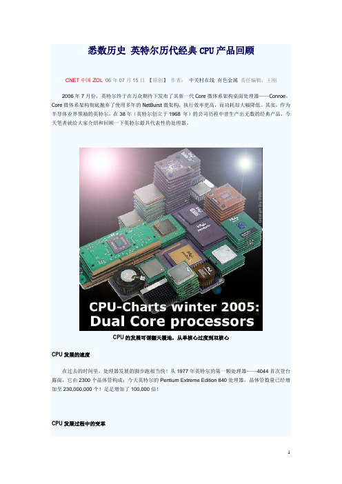
悉数历史英特尔历代经典CPU产品回顾CNET中国·ZOL06年07月15日【原创】作者:中关村在线有色金属责任编辑:王刚2006年7月份,英特尔终于在万众期待下发布了其新一代Core微体系架构桌面处理器——Conroe。
Core微体系架构彻底抛弃了使用多年的NetBurst微架构,执行效率更高,而功耗却大幅降低。
其实,作为半导体业界领袖的英特尔,在38年(英特尔创立于1968 年)的公司历程中曾生产出无数的经典产品,今天笔者就给大家介绍和回顾一下英特尔最具代表性的处理器。
CPU的发展可谓翻天覆地,从单核心过度到双核心CPU发展的速度在过去的时间里,处理器发展的脚步跑相当快!从1977年英特尔的第一颗处理器——4044首次登台露面,它由2300个晶体管构成;今天英特尔的Pentium Extreme Edition 840处理器,晶体管数量已经增加至230,000,000个!足足增加了100,000倍!CPU发展过程中的变革2006年,英特尔的LGA775平台已经成为市场主流;双核心也加入了CPU这个大家庭。
无疑,大家手中的CPU越来越“快”了。
本次,我们比较了从CPU诞生到现今CPU,从Sokect 370到LGA775,时钟频率从1MHz出头到现在最高的3.8GHz!介绍完了一些CPU发展的背景知识,现在就带大家去看看CPU是怎样从无到有,并且一步步发展起来的。
根据网络的记忆,笔者把它分为了几个发展阶段。
注意,这并非按照教科书去划分,而是根据我们的记忆。
CPU发展的初级阶段1971年1月,英特尔公司的霍夫(Marcian E.Hoff)研制成功4位微处理器芯片Intel 4004,标志着第一代微处理器问世,微处理器和微机时代从此开始。
正因为发明了微处理器,霍夫被英国《经济学家》杂志列为“二战以来最有影响力的7位科学家”之一。
英特尔的第一颗处理器——40044004当时只有2300个晶体管,是个四位系统,时钟频率仅为108KHz,每秒执行6万条指令(0.06 MIPs)。
cpu参数简介

CPU简介中央处理器是英语“Central Processing Unit”的缩写,即CPU,CPU一般由逻辑运算单元、控制单元和存储单元组成。
在逻辑运算和控制单元中包括一些寄存器,这些寄存器用于CPU在处理数据过程中数据的暂时保存,简单的讲是由控制器和运算器二部分组成。
性能指标·主频主频也叫时钟频率,单位是MHz,用来表示CPU的运算速度。
CPU的主频=外频×倍频系数。
很多人认为主频就决定着CPU的运行速度,这不仅是个片面的认识,而且对于服务器来讲,这个认识也出现了偏差。
至今,没有一条确定的公式能够实现主频和实际的运算速度两者之间的量值关系,即使是两大处理器厂家Intel和AMD,在这点上也存在着很大的争议,我们从Intel的产品的发展趋势,可以看出Intel很注重加强自身主频的发展。
像其他的处理器生产厂家,有人曾经拿过一块1G的全美达来做比较,它的运行效率相当于2G的Intel处理器。
所以,CPU的主频与CPU实际的运算能力是没有直接关系的,主频表示在CPU内数字脉冲信号震荡的速度。
在Intel的处理器产品中,我们也可以看到这样的例子:1 GHz Itanium芯片能够表现得差不多跟2.66 GHz Xeon/Opteron一样快,或是1.5 GHz Itanium 2大约跟4 GHz Xeon/Opteron一样快。
CPU的运算速度还要看CPU的流水线的各方面的性能指标。
当然,主频和实际的运算速度是有关的,只能说主频是CPU性能表现的一个方面,而不能代表CPU的整体性能。
·外频外频是CPU的基准频率,单位也是MHz。
CPU的外频决定着整块主板的运行速度。
说白了,在台式机中,我们所说的超频,都是超CPU的外频(当然一般情况下,CPU的倍频都是被锁住的)相信这点是很好理解的。
但对于服务器CPU来讲,超频是绝对不允许的。
前面说到CPU 决定着主板的运行速度,两者是同步运行的,如果把服务器CPU超频了,改变了外频,会产生异步运行,(台式机很多主板都支持异步运行)这样会造成整个服务器系统的不稳定。
微处理器
因特尔Intel桌面处理器CPU历史回顾(组图)2010年08月09日星期一下午 10:5110年前Pentium 处理器的诞生,从当初 60MHz主频到今天的主流3066MHz主频,而双核时代的到来,为PC技术增加了一道“彩虹”,20年可以改变缔造很多经典,我们仅从处理器CPU频率变化就足以让世人耳目一惊。
而在桌面处理器CPU领域,Intel具有哪些最值得我们回顾的产品呢?intel处理器CPU型号大全。
1971年:4004 微处理器4004 是Intel第一款微处理器,也是世界上第一款商用处理器,4004的诞生要归根于Busicom 计算器,因为当初这款款微处理器是作为日本计算器制造商 Busicom项目的一部分,开发一套用于可编程计算器家族的芯片,Busicom最初为这个计划提供了12种定制的芯片,Busicom 向Intel支付了 60,000 美元,因而获得了该微处理器所有权,之后Intel 提出用 60,000 美元换回微处理器设计的所有权,Busicom 同意了英特尔的请求,并且于1971 年 11 月 15日,Intel面向全球市场推出了 4004 处理器,该处理器拥有2,300晶体管数量,速度为108 KHz,当时售价为 299 美元。
4004 微处理器1972 年:8008 微处理器8008是Intel在1972年推出的,它的性能是4004的两倍,拥有3,500晶体管数量,速度为200 KHz,并且于1974年被一款名为 Mark-8 的设备采用,Mark-8 是第一批家用计算机之一,此时台式机基本上形成了一个最初雏形。
8008 微处理器1974 年:8080 微处理器Intel在1974年推出了性能更强大的8080处理器,拥有6,000晶体管数量,速度为2 MHz。
8080是第一款个人计算机 Altair 的大脑。
在当时,计算机爱好者花费 395 美元即可购得Altair 套件,之后的数月内,Altair 的销售量达到数万台,造成了电脑销售历史上第一次缺货现象。
MIPS CPU详细介绍

MIPS CPU详细介绍MIPS是世界上很流行的一种RISC处理器。
MIPS的意思是“无内部互锁流水级的微处理器”(Microprocessor without interlocked piped stages),其机制是尽量利用软件办法避免流水线中的数据相关问题。
它最早是在80年代初期由斯坦福(Stanford)大学Hennessy教授领导的研究小组研制出来的。
MIPS公司的R系列就是在此基础上开发的RISC工业产品的微处理器。
这些系列产品为很多计算机公司采用构成各种工作站和计算机系统。
MIPS技术公司是美国著名的芯片设计公司,它采用精简指令系统计算结构(RISC)来设计芯片。
和英特尔采用的复杂指令系统计算结构(CISC)相比, RISC 具有设计更简单、设计周期更短等优点,并可以应用更多先进的技术,开发更快的下一代处理器。
MIPS是出现最早的商业RISC架构芯片之一,新的架构集成了所有原来MIPS指令集,并增加了许多更强大的功能。
1986年推出R2000处理器,1988年推出R3000处理器,1991年推出第一款64位商用微处理器R4000。
之后,又陆续推出R8000(于 1994年)、R10000(于1996年)和R12000(于1997年)等型号。
1999年,MIPS公司发布MIPS 32和MIPS 64架构标准。
2000年,MIPS公司发布了针对MIPS 32 4Kc的新版本以及未来64位MIPS 64 20Kc处理器内核。
在MIPS芯片的发展过程中,SGI公司在1992年收购了MIPS计算机公司,1998年,MIPS公司又脱离了SGI,成为MIPS技术公司; MIPS32 4KcTM 处理器是采用MIPS技术特定为片上系统(System-On-a-Chip)而设计的高性能、低电压32位MIPS RISC 内核。
采用MIPS32TM体系结构,并且具有R4000存储器管理单元(MMU)以及扩展的优先级模式,使得这个处理器与目前嵌入式领域广泛应用的 R3000和R4000系列(32位)微处理器完全兼容.新的 64 位 MIPS 处理器是RM9000x2,从“x2”这个标记判断,它包含了不是一个而是两个均具有集成二级高速缓存的64位处理器。
CaviumOCTEON1

CaviumOCTEON11 Cavium OCTEON本⽂主要参考Cavium的programmer guide和CPU的硬件⽂档,涉及的内容主要包括Cavium的收发包流程以及针对收发包过程中的特性来进⾏性能上的调整。
⾸先从⼀般的包收发过程来说,⼀般情况下,⽹卡收到数据包后通过DMA映射到指定的内存位置,然后中断通知CPU来取数据包,经过⼏次内存拷贝后到达协议栈。
为了加速包的处理效率,⼀些CPU采⽤各种协处理器来帮助完成包的处理,经过多年的发展逐渐形成了以FreeScal Cavium Netlogic⼏家以RICS的MIPS架构为主流的NP处理器。
相⽐于通⽤处理器所⾯对的各种各样的需求,⽹络处理器⾯对的应⽤需求是有限的,因此⽹络处理器逐渐形成了除了收发包流程加速的协处理器外的针对类似于加密解密⼀类VPN SSL应⽤的加速协处理器。
在Cavium中,前者主要是指:SSO(POW)和PKO,后者则有相应的处理引擎。
2 OCTEON COPROCESSERCavium的OCTEON为⽹络做了⼤量优化,主要包括数量众多的协处理器,不同的协处理器完成特定的任务,⼤⼤简化了软件的复杂度提⾼了性能,并且能够从硬件上保证⼀些特性⽐如包保序。
如图是OCTEON的Arch:主要有:FPA PIP/IPD SSO PKO RAID_Engine FAU2.1 FPAFPA-Free Pool Alloctor主要负责分配收发包过程中的packet work entry以及packet的data buffer和PKO command buffer。
对FPA的操作主要有三种:buffer_allocte(synchronous): core会等待可⽤的buffer返回或者是返回的NULLbuffer_allocte(asynchronous): core不会等待buffer地址返回,⽽是在之后的时间⾥会从特定位置接受到buffer地址buffer_free(synchronous): 这个操作会把buffer地址返还到特定的FPA poolFPA的alloc free操作1. static inline void *cvmx_fpa_alloc(uint64_t pool) {2. adress = cvmx_read_csr(CVMX_ADDR_DID(CVMX_FULL_DID(CMVX_OCT_DID_FPA, pool)));3. }4.5. static inline void cmvx_fpa_free(......) {6. newptr.u64 = cvmx_ptr_to_phys(ptr);7. newptr.sfilldidispace.didspace = CVMX_ADDR_DIDSPACE(CVMX_FULL_DID(CVMX_OCT_DID_FPA,8. pool));9. cvmx_write_io(newptr.u64, unm_cache_lines);10. }FPA的initialize,cvmx-helper-fpa.c1. int cvmx_helper_initialize_fpa(.....) {2. return __cvmx_helper_initialize_fpa(3. CVMX_FPA_PACKET_POOL, cvmx_fpa_packet_pool_size_get(), packet_buffers,4. CVMX_FPA_WQE_POOL, CVMX_FPA_WQE_POOL_SIZE, work_queue_entries,5. CVMX_FPA_OUTPUT_BUFFER_POOL, CVMX_FPA_OUTPUT_BUFFER_POOL_SIZE, pko_buffers,6. CVMX_FPA_TIMER_POOL, CVMX_FPA_TIMER_POOL_SIZE, tim_buffers,7. CVMX_FPA_DFA_POOL, CVMX_FPA_DFA_POOL_SIZE, dfa_buffers,8. }在__cvmx_helper_initialize_fpa_pool()有我们需要的重要细节:在原来的SDK中时这样的:1. memory = cvmx_bootmem_alloc(buffer_size * buffers, align);但是代码却是这样:1. memory = KMALLOC(buffer_size*buffers + CVMX_CACHE_LINE_SIZE);区别在于cvmx_bootmeme_alloc()和KMALLOC()分别是在哪⾥分配的内存。
- 1、下载文档前请自行甄别文档内容的完整性,平台不提供额外的编辑、内容补充、找答案等附加服务。
- 2、"仅部分预览"的文档,不可在线预览部分如存在完整性等问题,可反馈申请退款(可完整预览的文档不适用该条件!)。
- 3、如文档侵犯您的权益,请联系客服反馈,我们会尽快为您处理(人工客服工作时间:9:00-18:30)。
应用于MIPS内核的OCTEON家族处理器介绍由技术编辑archive1 于星期五, 2014-07-04 11:24 发表放眼现今的网络、安全、无线及存储应用系统,对于最高性能及最低功耗的优质处理器需求持续升高。
Cavium Netowrks公司的OCTEON家族处理器经过高度优化,相当适合control-plane、data-plane应用或两者的混合,以优异性能提供网络、安全、无线及存储等应用最佳的选择。
OCTEON和OCTEON Plus处理器已被大多数的网通OEM厂所使用,凭借低成本以及低功耗等优势带来市场最领先的性能。
OCTEON处理器介绍OCTEON系列产品包括了三代且软件完全兼容、高度集成的多内核处理器:OCTEON® (CN3XXX)、OCTEON® Plus (CN5XXX)及OCTEON II (CN6XXX)。
这些处理器在优化之下提供了高性能、高带宽以及低功耗。
OCTEON处理器可应用于control-plan、data-plan 或是两者的混合。
OCTEON处理器提供了最佳的解决方案,包含智能网络、无线和100Mbps 到40Gbps的存储应用。
OCTEON全系列产品都共享相同的架构,使得全系列处理器软件都能兼容。
OCTEON处理器的区别基于下列几项:●cnMIPS®的内核数目●内核频率及internal interconnect●I/O接口的种类和数目●硬件加速器的种类和数目●高速缓存的容量以及结合性每个OCTEON产品都提供一组功能组(feature set),让应用目标能有最好的功能和性能。
编写好的软件可应用在不同的型号,只要它们有相同的功能(feature)。
OCTEON系列处理器特色OCTEON系列处理器的特色如下所示:●Custom-designed dual issue MIPS64 release 2cores,伴随着Cavium Netowrks创新的指令以提高性能●1到32内核的处理器提供最广泛的性能、功耗以及价格的选择性,同时提供全面的软件兼容性●内置的硬件加速器大幅提升应用上的性能、负载平衡以及同步处理●有着DMA引擎的高速内部连结,优化了OCTEON处理器的数据流量●集成的I/O接口和内存控制器能减少BOM成本及缩小产品的设计●简明的软件架构基于标准的C/C++编码,GNU toolchains,业界标准的操作系统,及optimized software stacks因为有了硬件加速器、灵活的软件架构、标准的MIPS64、toolchains、Packet-linked locks、scaling support和操作系统,使得软件开发的复杂性缩至最小OCTEON处理器的优点●内置了硬件加速器●每个内核专属的加解密处理器●芯片上各单元的内部连结●Cavium Networks特有的专属指令集●阶梯式的高速缓存OCTEON系列产品目标应用OCTEON处理器被使用在各式各样的OEM设备。
例如:●路由器●交换器●集成式管理器●内容感知交换器●应用感知网关器●三合一宽带网关器●无线网络存取集成设备●基站●内核网络设备●存储网络设备, 存储系统●服务器及智能网卡OCTEON系列产品主要特色OCTEON系列产品主要特色简述如下:32个内核,速度达1.5 GHzOCTEON家族的多内核处理器最多支持到32个cnMIPS内核,其速度从300MHz到1.5GHz。
●OCTEON和OCTEON Plus的产品支持1到16个内核,速度从300MHz到800MHz ●OCTEON II的产品最多可至32内核,速度高达1.5GHz硬件加速单元器--多重的硬件加速器内建在每个OCTEON处理器。
这些硬件加速器减轻了内核的负载,降低软件开发的费用和复杂度。
这些加速器包括了打包处理加速器、加解密处理加速器、应用程序加速器、特制化的加速器。
专用的DMA引擎专用的DMA引擎让每一个硬件加速器都有存取内存的功能。
某些型号的处理器提供了额外的存储器到PCI PCIe®/PCI/PCI-X® DMA引擎。
高速互连硬件单元和内核是高速互连的。
这些互相连结在与内核同样的频率下工作。
每个内部连结是由多个总线偕同流水线操作技术以及复杂的硬件调停逻辑所组成的。
总线的带宽和布置经过了最优化,使得数据传输更有效率,也消除潜在的瓶颈。
有些OCTEON II的型号含有cross-bar hyper-connect的技术使其内核数可达32或更多。
业界标准的开发工具和操作系统业界标准的开发工具(GCC, GDB)和操作系统(包括SMP Linux®)都已被用在OCTEON处理器的内核、硬件加速器、以及Cavium Networks-specific说明书。
使用者可以方便地编写C/C++程序,并且可以继续沿用现有的软件。
在MISP64和MIPS32 ISA架构下编写的软件都可以延续使用。
灵活的软件架构因OCTEON有良好的硬件架构,使其在软件设计上非常的灵活,包括当需要更多性能时聚集内核运算能力。
常见的配置是data-plane加上control-plane。
在这种配置中,一组内核运行data-plane应用,另一组内核运行SMP Linux或其它通用的操作系统提供control-plane功能。
如果需要的话,可以将任意内核加至data-plane,以获得线性的性能增强。
新型的软件开发因为有了硬件加速器、灵活的软件架构、标准的MIPS64 ISA、业界标准的toolchains和操作系统,软件开发的复杂度被缩至最小。
Cavium Networks提供了软件开发套件(SDK)。
该SDK包括了GNU C/C++编译器和其它开发工具、C语言的APIs、一个简单的执行器,它可以在没有任何操作系统下执行代码、以及Cavium Networks SMP Linux。
Cavium Networks还提供可选配的软件组合以支持更复杂的功能。
打包管理加速器打包的传送与接收是由可配置型软件的打包管理加速器所自动控制的。
加速的项目包含:●打包数据缓冲器自动配置与释放●Layer-2至layer-4打包表头解析,例外检查以及checksum的计算●可达七组支持VLAN stacking的打包流向分类●进入处理器的打包数据自动存储于L2/DRAM●打包的顺序和排序由硬件自动管理,不需要软件做特别的锁定●打包数据的传送由硬件加速器来管理TCP/UDP加速器TCP/UDP的加速功能包括:●打包管理的加速●收到打包时自动检查表头●传送时自动产生TCP/UDP checksum●Timer单元有效支持TCP重送的实现每个内核硬件加速安全算法*可选配的内核安全引擎加速了共通的安全算法。
(请参阅HRM的完整硬件加速算法列表)在下面的列表中,两个星号(**)表示该安全算法只存在特定的安全引擎中。
OCTEON的硬件加速安全算法包括:●强大的乘法累加单元可快速处理RSA和Diffie-Hellman运算所需要的模指数运算●Security hash算法:MD5, SHA-1, SHA-224, SHA-256,SHA-384, and SHA-512, AES XCBC, HMAC⎫●Symmetric cryptographic算法:- 3DES and DES in ECB and CBC modes⎫- AES in CBC, ECB, CTR, LRW, ICM, XTS,GCM, and CCM modes⎫- RC4⎫- KASUMI** (OCTEON Plus, OCTEON II)⎫- SNOW 3G** (OCTEON II)⎫- SMS4** (OCTEON II)⎫●Asymmetric key operations:- RSA, DSA, DH⎫●TKIP Operations: TKIP●Galois field multiplication (可同时用于像SNOW3G的安全性以及RAID计算)每个内核CRC引擎每个内核的CRC引擎加速产生了CRC:●硬件CRC计算(最多到32位):例如加速AAL2协议处理的CRC10以及加速AAL5协议处理的CRC32●CRC硬件同时也可以加速ROHC(Robust Header Compression)协议处理以及iSCSI checksum的计算和验证FIPS认证支持其它的特色使得高级FIPS (Federal Information Processing Standards)的认证更容易,包括:●NIST-认证过的算法●安全密码硬件装置RNG(Random Number Generator)。
此装置被设计为处理即将到来的FIPS标准●为了安全金钥而设的片上内存安全*,此内存无法通过I/O接口存取●特别设置的管脚以消除所有存储的金钥●受限制的PCI主机接入存储应用加速存储应用的加速包括:●RAID引擎*:RAID5及RAID6的RAID/XOR加速●每个内核专属的安全引擎*●Galois field乘法(包含在每个内核的安全加速)同样可用于RAID计算●De-duplication加速其它架构上的特色包括了下列清单:●MIPS64发布2整数ISA●额外的Cavium Networks特有专属指令集加强了MIPS内核以创造cnMIPS内核。
这些特有的指令大部分都是由C/C++所自动产生的●Dual-issue ALU与额外的安全加速协处理器单元。
结合了两个指令与额外的安全单元,在一个周期内,两个以上的运算是有可能同时被执行的●阶梯式高速缓存包括:- L2快取与EEC保护,范围从256KB至2MB(OCTEON II:最多可达4MB),由内核与I/O 子系统共享⎫- L1指令快取(Icache)与奇偶保护,每内核32KB(OCTEON II:最多可达37KB)⎫- L1数据快取(Dcache)与奇偶保护,每内核8KB至16KB(OCTEON II:最多可达32KB)⎫●32-entry至64-entry的TLB(OCTEON II:最多可有128-entry)支持:- 可变的页大小从4KB至256MB⎫- 读取和执行抑制了每页选择(用于防止溢位攻击和恶意代码)⎫●内存的选项包括:- DDR2从DDR2-400至DDR2-800(OCTEON与OCTEON Plus)⎫- DDR3最高可达DDR3-1600(OCTEON II)⎫●每个内核的写入缓冲器与aggressive写入相结合,限制内存的写入次数以减少不必要的总线传输●业界标准的I/O接口:XAUI*, SPI-4.2*, PCIe*, PCI/PCI-X*, SGMII*,RGMII*, GMII*, MII*, (OCTEON II:serial RapidIO®* (sRIO), and Interlaken*)●支持NOR及NAND*内存●从NOR内存启动(CN52XX支持从NAND启动)●Misc I/O包括:UARTs, USB 2.0* (包含PHY),TDM/PCM*, TWSI, SMI/MDIO, MII*, Boot Bus,GPIOs, LEDs●PCIE/PCI/PCI-X的DMA引擎*用在DMA与PCI主机内存存取或是从内存直接至内存●样式内存控制器*:用于连接样式内存至内核以及字符串样式比对引擎图1:以理想化的方式将OCTEON芯片上所有的硬件单元全部显示,此图也同时展示出只在特定型号才有的硬件单元。