半导体物理与器件第四版课后习题答案4
半导体物理与器件(尼曼第四版)答案
半导体物理与器件(尼曼第四版)答案第一章:半导体材料与晶体1.1 半导体材料的基本特性半导体材料是一种介于导体和绝缘体之间的材料。
它的基本特性包括:1.带隙:半导体材料的价带与导带之间存在一个禁带或带隙,是电子在能量上所能占据的禁止区域。
2.拉伸系统:半导体材料的结构是由原子或分子构成的晶格结构,其中的原子或分子以确定的方式排列。
3.载流子:在半导体中,存在两种载流子,即自由电子和空穴。
自由电子是在导带上的,在外加电场存在的情况下能够自由移动的电子。
空穴是在价带上的,当一个价带上的电子从该位置离开时,会留下一个类似电子的空位,空穴可以看作电子离开后的痕迹。
4.掺杂:为了改变半导体材料的导电性能,通常会对其进行掺杂。
掺杂是将少量元素添加到半导体材料中,以改变载流子浓度和导电性质。
1.2 半导体材料的结构与晶体缺陷半导体材料的结构包括晶体结构和非晶态结构。
晶体结构是指材料具有有序的周期性排列的结构,而非晶态结构是指无序排列的结构。
晶体结构的特点包括:1.晶体结构的基本单位是晶胞,晶胞在三维空间中重复排列。
2.晶格常数是晶胞边长的倍数,用于描述晶格的大小。
3.晶体结构可分为离子晶体、共价晶体和金属晶体等不同类型。
晶体结构中可能存在各种晶体缺陷,包括:1.点缺陷:晶体中原子位置的缺陷,主要包括实际缺陷和自间隙缺陷两种类型。
2.线缺陷:晶体中存在的晶面上或晶内的线状缺陷,主要包括位错和脆性断裂两种类型。
3.面缺陷:晶体中存在的晶面上的缺陷,主要包括晶面位错和穿孔两种类型。
1.3 半导体制备与加工半导体制备与加工是指将半导体材料制备成具有特定电性能的器件的过程。
它包括晶体生长、掺杂、薄膜制备和微电子加工等步骤。
晶体生长是将半导体材料从溶液或气相中生长出来的过程。
常用的晶体生长方法包括液相外延法、分子束外延法和气相外延法等。
掺杂是为了改变半导体材料的导电性能,通常会对其进行掺杂。
常用的掺杂方法包括扩散法、离子注入和分子束外延法等。
半导体物理与器件第四版课后习题答案4复习进程
m* E
mo
2
o 13.6
s
0.067 13.6
2
13.1
or E 0.0053 eV
_______________________________________
4.17 (a) E c E F
kT ln N c no
只供学习与交流
此文档仅供收集于网络,如有侵权请联系网站删除
19
2.8 10
0.0259 ln
4.11
只供学习与交流
E E Fi
midgap
1 kT ln N
2
Nc
1
1.04 1019
kT ln 2
2.8 1019
0.4952 kT
T (K)
200 400 600
kT (eV)
0.01727 0.03453 0.0518
( E Fi E midgap )(eV)
0.0086 0.0171 0.0257
19
2.8 10 1.04 10
3
T
300
1.12 exp
0.0259 T 300
2.5 10 23 2.912 10 38
3
T
300
1.12 300 exp
0.0259 T
By trial and error, T
367.5 K
3
2.912 10 38 T exp 1.12 300
300
0.0259 T
E E Fi
midgap
0.0128 eV
*
Germanium: m p 0.37mo ,
*
m n 0.55mo
E E Fi
midgap
半导体物理与器件第四版课后习题标准答案

半导体物理与器件第四版课后习题答案————————————————————————————————作者:————————————————————————————————日期:2______________________________________________________________________________________3Chapter 33.1If o a were to increase, the bandgap energy would decrease and the material would beginto behave less like a semiconductor and morelike a metal. If o a were to decrease, the bandgap energy would increase and thematerial would begin to behave more like an insulator._______________________________________ 3.2Schrodinger's wave equation is:()()()t x x V x t x m ,,2222ψ⋅+∂ψ∂-η()tt x j ∂ψ∂=,ηAssume the solution is of the form:()()⎥⎥⎦⎤⎢⎢⎣⎡⎪⎪⎭⎫ ⎝⎛⎪⎭⎫ ⎝⎛-=ψt E kx j x u t x ηexp , Region I: ()0=x V . Substituting theassumed solution into the wave equation, we obtain:()⎥⎥⎦⎤⎢⎢⎣⎡⎪⎪⎭⎫ ⎝⎛⎪⎭⎫ ⎝⎛-⎩⎨⎧∂∂-t E kx j x jku x m ηηexp 22 ()⎪⎭⎪⎬⎫⎥⎥⎦⎤⎢⎢⎣⎡⎪⎪⎭⎫ ⎝⎛⎪⎭⎫ ⎝⎛-∂∂+t E kx j x x u ηexp()⎥⎥⎦⎤⎢⎢⎣⎡⎪⎪⎭⎫ ⎝⎛⎪⎭⎫ ⎝⎛-⋅⎪⎭⎫ ⎝⎛-=t E kx j x u jE j ηηηexp which becomes()()⎥⎥⎦⎤⎢⎢⎣⎡⎪⎪⎭⎫ ⎝⎛⎪⎭⎫ ⎝⎛-⎩⎨⎧-t E kx j x u jk m ηηexp 222()⎥⎥⎦⎤⎢⎢⎣⎡⎪⎪⎭⎫ ⎝⎛⎪⎭⎫ ⎝⎛-∂∂+t E kx j x x u jk ηexp 2()⎪⎭⎪⎬⎫⎥⎥⎦⎤⎢⎢⎣⎡⎪⎪⎭⎫ ⎝⎛⎪⎭⎫ ⎝⎛-∂∂+t E kx j x x u ηexp 22()⎥⎥⎦⎤⎢⎢⎣⎡⎪⎪⎭⎫ ⎝⎛⎪⎭⎫ ⎝⎛-+=t E kx j x Eu ηexp This equation may be written as()()()()0222222=+∂∂+∂∂+-x u mE x x u x x u jk x u k ηSetting ()()x u x u 1= for region I, the equation becomes: ()()()()021221212=--+x u k dx x du jk dxx u d α where222ηmE=αQ.E.D.In Region II, ()O V x V =. Assume the same form of the solution:()()⎥⎥⎦⎤⎢⎢⎣⎡⎪⎪⎭⎫ ⎝⎛⎪⎭⎫ ⎝⎛-=ψt E kx j x u t x ηexp , Substituting into Schrodinger's wave equation, we find:()()⎥⎥⎦⎤⎢⎢⎣⎡⎪⎪⎭⎫ ⎝⎛⎪⎭⎫ ⎝⎛-⎩⎨⎧-t E kx j x u jk m ηηexp 222()⎥⎥⎦⎤⎢⎢⎣⎡⎪⎪⎭⎫ ⎝⎛⎪⎭⎫ ⎝⎛-∂∂+t E kx j x x u jk ηexp 2()⎪⎭⎪⎬⎫⎥⎥⎦⎤⎢⎢⎣⎡⎪⎪⎭⎫ ⎝⎛⎪⎭⎫ ⎝⎛-∂∂+t E kx j x x u ηexp 22()⎥⎥⎦⎤⎢⎢⎣⎡⎪⎪⎭⎫ ⎝⎛⎪⎭⎫ ⎝⎛-+t E kx j x u V O ηexp()⎥⎥⎦⎤⎢⎢⎣⎡⎪⎪⎭⎫ ⎝⎛⎪⎭⎫ ⎝⎛-=t E kx j x Eu ηexp This equation can be written as:______________________________________________________________________________________4()()()2222xx u x x u jk x u k ∂∂+∂∂+- ()()02222=+-x u mEx u mV O ηη Setting ()()x u x u 2= for region II, this equation becomes()()dx x du jkdx x u d 22222+()022222=⎪⎪⎭⎫ ⎝⎛+--x u mV k O ηα where again222ηmE=αQ.E.D._______________________________________ 3.3We have ()()()()021221212=--+x u k dx x du jk dxx u d α Assume the solution is of the form: ()()[]x k j A x u -=αexp 1 ()[]x k j B +-+αexpThe first derivative is()()()[]x k j A k j dxx du --=ααexp 1 ()()[]x k j B k j +-+-ααexpand the second derivative becomes()()[]()[]x k j A k j dxx u d --=ααexp 2212()[]()[]x k j B k j +-++ααexp 2Substituting these equations into the differential equation, we find()()[]x k j A k ---ααexp 2()()[]x k j B k +-+-ααexp 2(){()[]x k j A k j jk --+ααexp 2()()[]}x k j B k j +-+-ααexp ()()[]{x k j A k ---ααexp 22 ()[]}0exp =+-+x k j B α Combining terms, we obtain()()()[]222222αααα----+--k k k k k ()[]x k j A -⨯αexp()()()[]222222αααα--++++-+k k k k k()[]0exp =+-⨯x k j B α We find that00= Q.E.D.For the differential equation in ()x u 2 and theproposed solution, the procedure is exactly the same as above._______________________________________ 3.4We have the solutions()()[]x k j A x u -=αexp 1()[]x k j B +-+αexp for a x <<0 and()()[]x k j C x u -=βexp 2()[]x k j D +-+βexp for 0<<-x b .The first boundary condition is ()()0021u u =which yields0=--+D C B AThe second boundary condition is201===x x dx dudx du which yields()()()C k B k A k --+--βαα ()0=++D k βThe third boundary condition is ()()b u a u -=21 which yields()[]()[]a k j B a k j A +-+-ααexp exp ()()[]b k j C --=βexp ()()[]b k j D -+-+βexp______________________________________________________________________________________5and can be written as()[]()[]a k j B a k j A +-+-ααexp exp ()[]b k j C ---βexp ()[]0exp =+-b k j D βThe fourth boundary condition isbx a x dx dudx du -===21 which yields()()[]a k j A k j --ααexp()()[]a k j B k j +-+-ααexp()()()[]b k j C k j ---=ββexp()()()[]b k j D k j -+-+-ββexp and can be written as()()[]a k j A k --ααexp()()[]a k j B k +-+-ααexp ()()[]b k j C k ----ββexp()()[]0exp =+++b k j D k ββ_______________________________________ 3.5(b) (i) First point: πα=aSecond point: By trial and error, πα729.1=a (ii) First point: πα2=aSecond point: By trial and error, πα617.2=a _______________________________________ 3.6(b) (i) First point: πα=aSecond point: By trial and error, πα515.1=a (ii) First point: πα2=aSecond point: By trial and error, πα375.2=a _______________________________________ 3.7ka a aaP cos cos sin =+'ααα Let y ka =, x a =α Theny x x xP cos cos sin =+'Consider dydof this function.()[]{}y x x x P dyd sin cos sin 1-=+⋅'- We find()()()⎭⎬⎫⎩⎨⎧⋅+⋅-'--dy dx x x dy dx x x P cos sin 112y dydx x sin sin -=-Theny x x x x x P dy dx sin sin cos sin 12-=⎭⎬⎫⎩⎨⎧-⎥⎦⎤⎢⎣⎡+-' For πn ka y ==,...,2,1,0=n 0sin =⇒y So that, in general,()()dkd ka d a d dy dxαα===0 And22ηmE=α SodkdEm mE dk d ⎪⎭⎫ ⎝⎛⎪⎭⎫ ⎝⎛=-22/122221ηηα This implies thatdk dE dk d ==0α for an k π= _______________________________________ 3.8(a) πα=a 1π=⋅a E m o 212η______________________________________________________________________________________6()()()()2103123422221102.41011.9210054.12---⨯⨯⨯==ππa m E o η19104114.3-⨯=J From Problem 3.5 πα729.12=aπ729.1222=⋅a E m o η()()()()2103123422102.41011.9210054.1729.1---⨯⨯⨯=πE18100198.1-⨯=J12E E E -=∆1918104114.3100198.1--⨯-⨯= 19107868.6-⨯=Jor 24.4106.1107868.61919=⨯⨯=∆--E eV(b) πα23=aπ2223=⋅a E m o η()()()()2103123423102.41011.9210054.12---⨯⨯⨯=πE18103646.1-⨯=J From Problem 3.5, πα617.24=aπ617.2224=⋅a E m o η()()()()2103123424102.41011.9210054.1617.2---⨯⨯⨯=πE18103364.2-⨯=J34E E E -=∆1818103646.1103364.2--⨯-⨯= 1910718.9-⨯=Jor 07.6106.110718.91919=⨯⨯=∆--E eV_______________________________________ 3.9(a) At π=ka , πα=a 1π=⋅a E m o 212η()()()()2103123421102.41011.9210054.1---⨯⨯⨯=πE19104114.3-⨯=JAt 0=ka , By trial and error, πα859.0=a o()()()()210312342102.41011.9210054.1859.0---⨯⨯⨯=πo E19105172.2-⨯=J o E E E -=∆11919105172.2104114.3--⨯-⨯= 2010942.8-⨯=Jor 559.0106.110942.81920=⨯⨯=∆--E eV (b) At π2=ka , πα23=aπ2223=⋅a E m o η()()()()2103123423102.41011.9210054.12---⨯⨯⨯=πE18103646.1-⨯=J At π=ka . From Problem 3.5,πα729.12=aπ729.1222=⋅a E m o η()()()()2103123422102.41011.9210054.1729.1---⨯⨯⨯=πE18100198.1-⨯=J 23E E E -=∆1818100198.1103646.1--⨯-⨯= 19104474.3-⨯=Jor 15.2106.1104474.31919=⨯⨯=∆--E eV_____________________________________________________________________________________________________________________________73.10(a) πα=a 1π=⋅a E m o 212η()()()()2103123421102.41011.9210054.1---⨯⨯⨯=πE19104114.3-⨯=JFrom Problem 3.6, πα515.12=aπ515.1222=⋅a E m o η()()()()2103123422102.41011.9210054.1515.1---⨯⨯⨯=πE1910830.7-⨯=J 12E E E -=∆1919104114.310830.7--⨯-⨯= 19104186.4-⨯=Jor 76.2106.1104186.41919=⨯⨯=∆--E eV(b) πα23=aπ2223=⋅a E m o η()()()()2103123423102.41011.9210054.12---⨯⨯⨯=πE18103646.1-⨯=JFrom Problem 3.6, πα375.24=aπ375.2224=⋅a E m o η()()()()2103123424102.41011.9210054.1375.2---⨯⨯⨯=πE18109242.1-⨯=J 34E E E -=∆1818103646.1109242.1--⨯-⨯=1910597.5-⨯=Jor 50.3106.110597.51919=⨯⨯=∆--E eV _____________________________________3.11(a) At π=ka , πα=a 1π=⋅a E m o 212η()()()()2103123421102.41011.9210054.1---⨯⨯⨯=πE19104114.3-⨯=J At 0=ka , By trial and error, πα727.0=a o π727.022=⋅a E m o o η()()()()210312342102.41011.9210054.1727.0---⨯⨯⨯=πo E19108030.1-⨯=J o E E E -=∆11919108030.1104114.3--⨯-⨯= 19106084.1-⨯=Jor 005.1106.1106084.11919=⨯⨯=∆--E eV (b) At π2=ka , πα23=aπ2223=⋅a E m o η()()()()2103123423102.41011.9210054.12---⨯⨯⨯=πE18103646.1-⨯=JAt π=ka , From Problem 3.6, πα515.12=aπ515.1222=⋅a E m o η()()()()2103423422102.41011.9210054.1515.1---⨯⨯⨯=πE1910830.7-⨯=J 23E E E -=∆191810830.7103646.1--⨯-⨯=______________________________________________________________________________________81910816.5-⨯=Jor 635.3106.110816.51919=⨯⨯=∆--E eV_______________________________________ 3.12For 100=T K,()()⇒+⨯-=-1006361001073.4170.124g E164.1=g E eV200=T K, 147.1=g E eV 300=T K, 125.1=g E eV 400=T K, 097.1=g E eV 500=T K, 066.1=g E eV 600=T K, 032.1=g E eV _______________________________________ 3.13The effective mass is given by1222*1-⎪⎪⎭⎫ ⎝⎛⋅=dk E d m ηWe have()()B curve dkEd A curve dk E d 2222>so that ()()B curve m A curve m **<_______________________________________ 3.14The effective mass for a hole is given by1222*1-⎪⎪⎭⎫ ⎝⎛⋅=dk E d m p η We have that()()B curve dkEd A curve dk E d 2222> so that ()()B curve m A curve m p p **<_______________________________________ 3.15Points A,B: ⇒<0dkdEvelocity in -x direction Points C,D: ⇒>0dkdEvelocity in +x directionPoints A,D: ⇒<022dk Ednegative effective massPoints B,C: ⇒>022dkEd positive effective mass_______________________________________ 3.16For A: 2k C E i =At 101008.0+⨯=k m 1-, 05.0=E eV Or()()2119108106.105.0--⨯=⨯=E JSo ()2101211008.0108⨯=⨯-C3811025.1-⨯=⇒CNow ()()38234121025.1210054.12--*⨯⨯==C m η 311044.4-⨯=kgor o m m ⋅⨯⨯=--*31311011.9104437.4 o m m 488.0=*For B: 2k C E i =At 101008.0+⨯=k m 1-, 5.0=E eV Or ()()2019108106.15.0--⨯=⨯=E JSo ()2101201008.0108⨯=⨯-C 3711025.1-⨯=⇒CNow ()()37234121025.1210054.12--*⨯⨯==C m η321044.4-⨯=kgor o m m ⋅⨯⨯=--*31321011.9104437.4o m m 0488.0=*_____________________________________________________________________________________________________________________________93.17For A: 22k C E E -=-υ()()()2102191008.0106.1025.0⨯-=⨯--C3921025.6-⨯=⇒C ()()39234221025.6210054.12--*⨯⨯-=-=C m η31108873.8-⨯-=kgor o m m ⋅⨯⨯-=--*31311011.9108873.8o m m 976.0--=* For B: 22k C E E -=-υ()()()2102191008.0106.13.0⨯-=⨯--C382105.7-⨯=⇒C()()3823422105.7210054.12--*⨯⨯-=-=C m η3210406.7-⨯-=kgor o m m ⋅⨯⨯-=--*31321011.910406.7o m m 0813.0-=*_______________________________________ 3.18(a) (i) νh E =or ()()341910625.6106.142.1--⨯⨯==h E ν1410429.3⨯=Hz(ii) 141010429.3103⨯⨯===νλc E hc 51075.8-⨯=cm 875=nm(b) (i) ()()341910625.6106.112.1--⨯⨯==h E ν 1410705.2⨯=Hz(ii) 141010705.2103⨯⨯==νλc410109.1-⨯=cm 1109=nm _______________________________________ 3.19(c) Curve A: Effective mass is a constantCurve B: Effective mass is positive around 0=k , and is negativearound 2π±=k ._______________________________________ 3.20()[]O O k k E E E --=αcos 1 Then()()()[]O k k E dkdE---=ααsin 1()[]O k k E -+=ααsin 1 and()[]O k k E dkEd -=ααcos 2122Then221222*11ηηαE dk Ed m o k k =⋅== or212*αE m η=_______________________________________ 3.21(a) ()[]3/123/24l t dnm m m =*()()[]3/123/264.1082.04o o m m =o dnm m 56.0=*(b)oo l t cn m m m m m 64.11082.02123+=+=*oo m m 6098.039.24+=o cnm m 12.0=*_______________________________________ 3.22(a) ()()[]3/22/32/3lh hh dp m m m +=*______________________________________________________________________________________10()()[]3/22/32/3082.045.0o o m m +=[]o m ⋅+=3/202348.030187.0o dpm m 473.0=*(b) ()()()()2/12/12/32/3lh hh lh hh cpm m m m m ++=* ()()()()om ⋅++=2/12/12/32/3082.045.0082.045.0 o cpm m 34.0=*_______________________________________3.23For the 3-dimensional infinite potential well, ()0=x V when a x <<0, a y <<0, and a z <<0. In this region, the wave equation is:()()()222222,,,,,,z z y x y z y x x z y x ∂∂+∂∂+∂∂ψψψ()0,,22=+z y x mEψηUse separation of variables technique, so let ()()()()z Z y Y x X z y x =,,ψSubstituting into the wave equation, we have222222zZXY y Y XZ x X YZ ∂∂+∂∂+∂∂ 022=⋅+XYZ mEηDividing by XYZ , we obtain021*********=+∂∂⋅+∂∂⋅+∂∂⋅ηmE z Z Z y Y Y x X X Let01222222=+∂∂⇒-=∂∂⋅X k x X k x X X xx The solution is of the form: ()x k B x k A x X x x cos sin += Since ()0,,=z y x ψ at 0=x , then ()00=Xso that 0=B .Also, ()0,,=z y x ψ at a x =, so that()0=a X . Then πx x n a k = where...,3,2,1=x n Similarly, we have2221y k y Y Y -=∂∂⋅ and 2221z k zZ Z -=∂∂⋅From the boundary conditions, we find πy y n a k = and πz z n a k = where...,3,2,1=y n and ...,3,2,1=z n From the wave equation, we can write022222=+---ηmE k k k z y xThe energy can be written as()222222⎪⎭⎫ ⎝⎛++==a n n n m E E z y x n n n z y x πη _______________________________________ 3.24The total number of quantum states in the 3-dimensional potential well is given (in k-space) by()332a dk k dk k g T ⋅=ππ where222ηmEk =We can then writeηmEk 2=Taking the differential, we obtaindE Em dE E m dk ⋅⋅=⋅⋅⋅⋅=2112121ηηSubstituting these expressions into the densityof states function, we have()dE EmmE a dE E g T ⋅⋅⋅⎪⎭⎫ ⎝⎛=212233ηηππ Noting thatπ2h=ηthis density of states function can be simplified and written as______________________________________________________________________________________()()dE E m h a dE E g T ⋅⋅=2/33324πDividing by 3a will yield the density of states so that()()E hm E g ⋅=32/324π _______________________________________ 3.25For a one-dimensional infinite potential well,222222k an E m n ==*πη Distance between quantum states()()aa n a n k k n n πππ=⎪⎭⎫ ⎝⎛=⎪⎭⎫ ⎝⎛+=-+11Now()⎪⎭⎫ ⎝⎛⋅=a dkdk k g T π2NowE m k n*⋅=21ηdE Em dk n⋅⋅⋅=*2211η Then()dE Em a dE E g n T ⋅⋅⋅=*2212ηπDivide by the "volume" a , so()Em E g n *⋅=21πηSo()()()()()EE g 31341011.9067.0210054.11--⨯⋅⨯=π ()EE g 1810055.1⨯=m 3-J 1-_______________________________________ 3.26(a) Silicon, o nm m 08.1=*()()c nc E E h m E g -=*32/324π()dE E E h m g kTE E c nc c c⋅-=⎰+*232/324π()()kT E E c nc cE E h m 22/332/33224+*-⋅⋅=π()()2/332/323224kT h m n⋅⋅=*π ()()[]()()2/33342/33123210625.61011.908.124kT ⋅⋅⨯⨯=--π ()()2/355210953.7kT ⨯=(i) At 300=T K, 0259.0=kT eV ()()19106.10259.0-⨯=2110144.4-⨯=J Then()()[]2/3215510144.4210953.7-⨯⨯=c g25100.6⨯=m 3- or 19100.6⨯=c g cm 3-(ii) At 400=T K, ()⎪⎭⎫⎝⎛=3004000259.0kT034533.0=eV()()19106.1034533.0-⨯=21105253.5-⨯=J Then()()[]2/32155105253.5210953.7-⨯⨯=c g2510239.9⨯=m 3-or 191024.9⨯=c g cm 3-(b) GaAs, o nm m 067.0=*()()[]()()2/33342/33123210625.61011.9067.024kT g c ⋅⋅⨯⨯=--π ()()2/3542102288.1kT ⨯=______________________________________________________________________________________(i) At 300=T K, 2110144.4-⨯=kT J()()[]2/3215410144.42102288.1-⨯⨯=c g2310272.9⨯=m 3- or 171027.9⨯=c g cm 3-(ii) At 400=T K, 21105253.5-⨯=kT J()()[]2/32154105253.52102288.1-⨯⨯=c g2410427.1⨯=m 3- 181043.1⨯=c g cm 3-_______________________________________ 3.27(a) Silicon, o p m m 56.0=* ()()E E h mE g p-=*υυπ32/324()dE E E h m g E kTE p⋅-=⎰-*υυυυπ332/324()()υυυπE kTE pE E h m 32/332/33224-*-⎪⎭⎫ ⎝⎛-=()()[]2/332/333224kT h mp-⎪⎭⎫ ⎝⎛-=*π ()()[]()()2/33342/33133210625.61011.956.024kT ⎪⎭⎫ ⎝⎛⨯⨯=--π ()()2/355310969.2kT ⨯=(i)At 300=T K, 2110144.4-⨯=kT J ()()[]2/3215510144.4310969.2-⨯⨯=υg2510116.4⨯=m 3- or 191012.4⨯=υg cm 3-(ii)At 400=T K, 21105253.5-⨯=kT J ()()[]2/32155105253.5310969.2-⨯⨯=υg2510337.6⨯=m 3-or 191034.6⨯=υg cm 3- (b) GaAs, o p m m 48.0=*()()[]()()2/33342/33133210625.61011.948.024kT g ⎪⎭⎫ ⎝⎛⨯⨯=--πυ ()()2/3553103564.2kT ⨯=(i)At 300=T K, 2110144.4-⨯=kT J ()()[]2/3215510144.43103564.2-⨯⨯=υg2510266.3⨯=m 3- or 191027.3⨯=υg cm 3-(ii)At 400=T K, 21105253.5-⨯=kT J()()[]2/32155105253.53103564.2-⨯⨯=υg2510029.5⨯=m 3-or 191003.5⨯=υg cm 3-_______________________________________ 3.28(a) ()()c nc E E h m E g -=*32/324π()()[]()c E E -⨯⨯=--3342/33110625.61011.908.124πc E E -⨯=56101929.1 For c E E =; 0=c g1.0+=c E E eV; 4610509.1⨯=c g m 3-J 1-2.0+=c E E eV;4610134.2⨯=m 3-J 1- 3.0+=c E E eV; 4610614.2⨯=m 3-J 1- 4.0+=c E E eV; 4610018.3⨯=m 3-J 1-(b) ()E E hm g p-=*υυπ32/324()()[]()E E -⨯⨯=--υπ3342/33110625.61011.956.024E E -⨯=υ55104541.4______________________________________________________________________________________For υE E =; 0=υg 1.0-=υE E eV; 4510634.5⨯=υg m 3-J 1-2.0-=υE E eV;4510968.7⨯=m 3-J 1-3.0-=υE E eV; 4510758.9⨯=m 3-J 1-4.0-=υE E eV;4610127.1⨯=m 3-J 1-_______________________________________ 3.29(a) ()()68.256.008.12/32/32/3=⎪⎭⎫ ⎝⎛==**pnc m m g g υ(b) ()()0521.048.0067.02/32/32/3=⎪⎭⎫ ⎝⎛==**pncmm g g υ_______________________________________3.30 Plot_______________________________________ 3.31(a) ()()()!710!7!10!!!-=-=i i i i i N g N g W()()()()()()()()()()()()1201238910!3!7!78910===(b) (i) ()()()()()()()()12!10!101112!1012!10!12=-=i W 66= (ii)()()()()()()()()()()()()1234!8!89101112!812!8!12=-=i W 495=_______________________________________ 3.32()⎪⎪⎭⎫ ⎝⎛-+=kT E E E f F exp 11(a) kT E E F =-, ()()⇒+=1exp 11E f ()269.0=E f(b) kT E E F 5=-, ()()⇒+=5exp 11E f()31069.6-⨯=E f (c) kT E E F 10=-, ()()⇒+=10exp 11E f()51054.4-⨯=E f_______________________________________ 3.33()⎪⎪⎭⎫ ⎝⎛-+-=-kT E E E f F exp 1111or()⎪⎪⎭⎫⎝⎛-+=-kT E E E f F exp 111(a) kT E E F =-, ()269.01=-E f (b) kT E E F 5=-, ()31069.61-⨯=-E f (c) kT E E F 10=-, ()51054.41-⨯=-E f_______________________________________ 3.34(a) ()⎥⎦⎤⎢⎣⎡--≅kT E E f F F exp c E E =; 61032.90259.030.0exp -⨯=⎥⎦⎤⎢⎣⎡-=F f 2kT E c +; ()⎥⎦⎤⎢⎣⎡+-=0259.020259.030.0exp F f 61066.5-⨯=kT E c +; ()⎥⎦⎤⎢⎣⎡+-=0259.00259.030.0exp F f 61043.3-⨯=23kT E c +; ()()⎥⎦⎤⎢⎣⎡+-=0259.020259.0330.0exp F f 61008.2-⨯=kT E c 2+; ()()⎥⎦⎤⎢⎣⎡+-=0259.00259.0230.0exp F f 61026.1-⨯=______________________________________________________________________________________(b) ⎥⎦⎤⎢⎣⎡-+-=-kT E E f F F exp 1111()⎥⎦⎤⎢⎣⎡--≅kT E E F exp υE E =; ⎥⎦⎤⎢⎣⎡-=-0259.025.0exp 1F f 51043.6-⨯= 2kT E -υ; ()⎥⎦⎤⎢⎣⎡+-=-0259.020259.025.0exp 1F f 51090.3-⨯=kT E -υ; ()⎥⎦⎤⎢⎣⎡+-=-0259.00259.025.0exp 1F f 51036.2-⨯=23kT E -υ;()()⎥⎦⎤⎢⎣⎡+-=-0259.020259.0325.0exp 1F f 51043.1-⨯= kT E 2-υ;()()⎥⎦⎤⎢⎣⎡+-=-0259.00259.0225.0exp 1F f 61070.8-⨯=_______________________________________ 3.35()()⎥⎦⎤⎢⎣⎡-+-=⎥⎦⎤⎢⎣⎡--=kT E kT E kT E E f F c F F exp exp and()⎥⎦⎤⎢⎣⎡--=-kT E E f F F exp 1()()⎥⎦⎤⎢⎣⎡---=kT kT E E F υexp So ()⎥⎦⎤⎢⎣⎡-+-kT E kT E F c exp()⎥⎦⎤⎢⎣⎡+--=kT kT E E F υexp Then kT E E E kT E F F c +-=-+υOr midgap c F E E E E =+=2υ_______________________________________ 3.3622222man E n πη= For 6=n , Filled state()()()()()2103122234610121011.92610054.1---⨯⨯⨯=πE18105044.1-⨯=Jor 40.9106.1105044.119186=⨯⨯=--E eVFor 7=n , Empty state()()()()()2103122234710121011.92710054.1---⨯⨯⨯=πE1810048.2-⨯=Jor 8.12106.110048.219187=⨯⨯=--E eVTherefore 8.1240.9<<F E eV_______________________________________ 3.37(a) For a 3-D infinite potential well ()222222⎪⎭⎫⎝⎛++=a n n n mE z y x πη For 5 electrons, the 5thelectron occupies the quantum state 1,2,2===z y x n n n ; so()2222252⎪⎭⎫ ⎝⎛++=a n n n m E z y x πη()()()()()21031222223410121011.9212210054.1---⨯⨯++⨯=π 1910761.3-⨯=Jor 35.2106.110761.319195=⨯⨯=--E eV For the next quantum state, which is empty, the quantum state is 2,2,1===z y x n n n . This quantum state is at the same energy, so 35.2=F E eV(b) For 13 electrons, the 13th electronoccupies the quantum state______________________________________________________________________________________3,2,3===z y x n n n ; so ()()()()()2103122222341310121011.9232310054.1---⨯⨯++⨯=πE 1910194.9-⨯=Jor 746.5106.110194.9191913=⨯⨯=--E eVThe 14th electron would occupy the quantum state 3,3,2===z y x n n n . This state is at the same energy, so 746.5=F E eV_______________________________________ 3.38The probability of a state at E E E F ∆+=1 being occupied is()⎪⎭⎫ ⎝⎛∆+=⎪⎪⎭⎫ ⎝⎛-+=kT E kT E E E f F exp 11exp 11111 The probability of a state at E E E F ∆-=2being empty is()⎪⎪⎭⎫ ⎝⎛-+-=-kT E E E f F 222exp 1111⎪⎭⎫ ⎝⎛∆-+⎪⎭⎫ ⎝⎛∆-=⎪⎭⎫ ⎝⎛∆-+-=kT E kT E kT E exp 1exp exp 111 or()⎪⎭⎫ ⎝⎛∆+=-kT E E f exp 11122 so ()()22111E f E f -= Q.E.D._______________________________________ 3.39(a) At energy 1E , we want01.0exp 11exp 11exp 1111=⎪⎪⎭⎫ ⎝⎛-+⎪⎪⎭⎫ ⎝⎛-+-⎪⎪⎭⎫ ⎝⎛-kT E E kT E E kT E E F F FThis expression can be written as01.01exp exp 111=-⎪⎪⎭⎫ ⎝⎛-⎪⎪⎭⎫ ⎝⎛-+kT E E kT E E F For()⎪⎪⎭⎫⎝⎛-=kT E E F 1exp 01.01Then()100ln 1kT E E F += orkT E E F 6.41+= (b)At kT E E F 6.4+=,()()6.4exp 11exp 1111+=⎪⎪⎭⎫ ⎝⎛-+=kT E E E f F which yields()01.000990.01≅=E f_______________________________________ 3.40 (a)()()⎥⎦⎤⎢⎣⎡--=⎥⎦⎤⎢⎣⎡--=0259.050.580.5exp exp kT E E f F F 61032.9-⨯=(b) ()060433.03007000259.0=⎪⎭⎫⎝⎛=kT eV31098.6060433.030.0exp -⨯=⎥⎦⎤⎢⎣⎡-=F f (c) ()⎥⎦⎤⎢⎣⎡--≅-kT E E f F F exp 1 ⎥⎦⎤⎢⎣⎡-=kT 25.0exp 02.0______________________________________________________________________________________or 5002.0125.0exp ==⎥⎦⎤⎢⎣⎡+kT ()50ln 25.0=kTor()()⎪⎭⎫⎝⎛===3000259.0063906.050ln 25.0T kTwhich yields 740=T K_______________________________________ 3.41 (a)()00304.00259.00.715.7exp 11=⎪⎭⎫ ⎝⎛-+=E for 0.304%(b) At 1000=T K, 08633.0=kT eV Then()1496.008633.00.715.7exp 11=⎪⎭⎫ ⎝⎛-+=E for 14.96%(c) ()997.00259.00.785.6exp 11=⎪⎭⎫⎝⎛-+=E for 99.7% (d)At F E E =, ()21=E f for alltemperatures_______________________________________ 3.42(a) For 1E E =()()⎥⎦⎤⎢⎣⎡--≅⎪⎪⎭⎫ ⎝⎛-+=kT E E kTE E E fF F11exp exp 11Then()611032.90259.030.0exp -⨯=⎪⎭⎫ ⎝⎛-=E fFor 2E E =,82.030.012.12=-=-E E F eV Then()⎪⎭⎫ ⎝⎛-+-=-0259.082.0exp 1111E for()⎥⎦⎤⎢⎣⎡⎪⎭⎫ ⎝⎛---≅-0259.082.0exp 111E f141078.10259.082.0exp -⨯=⎪⎭⎫ ⎝⎛-=(b) For 4.02=-E E F eV, 72.01=-F E E eV At 1E E =,()()⎪⎭⎫⎝⎛-=⎥⎦⎤⎢⎣⎡--=0259.072.0exp exp 1kT E E E f F or()131045.8-⨯=E f At 2E E =,()()⎥⎦⎤⎢⎣⎡--=-kT E E E f F 2exp 1⎪⎭⎫ ⎝⎛-=0259.04.0expor()71096.11-⨯=-E f_______________________________________ 3.43(a) At 1E E =()()⎪⎭⎫⎝⎛-=⎥⎦⎤⎢⎣⎡--=0259.030.0exp exp 1kT E E E f F or()61032.9-⨯=E f At 2E E =, 12.13.042.12=-=-E E F eV So()()⎥⎦⎤⎢⎣⎡--=-kT E E E f F 2exp 1⎪⎭⎫ ⎝⎛-=0259.012.1exp______________________________________________________________________________________or()191066.11-⨯=-E f(b) For 4.02=-E E F ,02.11=-F E E eV At 1E E =,()()⎪⎭⎫⎝⎛-=⎥⎦⎤⎢⎣⎡--=0259.002.1exp exp 1kT E E E f F or()181088.7-⨯=E f At 2E E =,()()⎥⎦⎤⎢⎣⎡--=-kT E E E f F 2exp 1⎪⎭⎫ ⎝⎛-=0259.04.0expor ()71096.11-⨯=-E f_______________________________________ 3.44()1exp 1-⎥⎦⎤⎢⎣⎡⎪⎪⎭⎫ ⎝⎛-+=kTE E E f Fso()()2exp 11-⎥⎦⎤⎢⎣⎡⎪⎪⎭⎫ ⎝⎛-+-=kT E E dE E df F⎪⎪⎭⎫ ⎝⎛-⎪⎭⎫⎝⎛⨯kT E E kT F exp 1 or()2exp 1exp 1⎥⎦⎤⎢⎣⎡⎪⎪⎭⎫ ⎝⎛-+⎪⎪⎭⎫ ⎝⎛-⎪⎭⎫⎝⎛-=kT E E kT E E kT dE E df F F (a) At 0=T K, For()00exp =⇒=∞-⇒<dE dfE E F()0exp =⇒+∞=∞+⇒>dEdfE E FAt -∞=⇒=dEdfE E F(b) At 300=T K, 0259.0=kT eVFor F E E <<,0=dE dfFor F E E >>, 0=dEdfAt F E E =,()()65.91110259.012-=+⎪⎭⎫ ⎝⎛-=dE df (eV)1-(c) At 500=T K, 04317.0=kT eVFor F E E <<, 0=dE dfFor F E E >>, 0=dEdfAt F E E =, ()()79.511104317.012-=+⎪⎭⎫ ⎝⎛-=dE df (eV)1- _______________________________________ 3.45(a) At midgap E E =,()⎪⎪⎭⎫ ⎝⎛+=⎪⎪⎭⎫ ⎝⎛-+=kTE kTE E E f gF2exp 11exp 11Si: 12.1=g E eV, ()()⎥⎦⎤⎢⎣⎡+=0259.0212.1exp 11E for()101007.4-⨯=E fGe: 66.0=g E eV______________________________________________________________________________________()()⎥⎦⎤⎢⎣⎡+=0259.0266.0exp 11E for()61093.2-⨯=E f GaAs: 42.1=g E eV ()()⎥⎦⎤⎢⎣⎡+=0259.0242.1exp 11E for()121024.1-⨯=E f(b) Using the results of Problem 3.38, the answers to part (b) are exactly the same as those given in part (a)._______________________________________ 3.46(a) ()⎥⎦⎤⎢⎣⎡--=kT E E f F F exp ⎥⎦⎤⎢⎣⎡-=-kT 60.0exp 108 or ()810ln 60.0+=kT()032572.010ln 60.08==kT eV()⎪⎭⎫⎝⎛=3000259.0032572.0Tso 377=T K(b) ⎥⎦⎤⎢⎣⎡-=-kT 60.0exp 106()610ln 60.0+=kT()043429.010ln 60.06==kT ()⎪⎭⎫⎝⎛=3000259.0043429.0Tor 503=T K_______________________________________ 3.47(a) At 200=T K,()017267.03002000259.0=⎪⎭⎫⎝⎛=kT eV⎪⎪⎭⎫ ⎝⎛-+==kTE E f FF exp 1105.019105.01exp =-=⎪⎪⎭⎫⎝⎛-kT E E F()()()19ln 017267.019ln ==-kT E E F 05084.0=eV By symmetry, for 95.0=F f , 05084.0-=-F E E eVThen ()1017.005084.02==∆E eV (b) 400=T K, 034533.0=kT eV For 05.0=F f , from part (a),()()()19ln 034533.019ln ==-kT E E F 10168.0=eV Then ()2034.010168.02==∆E eV_______________________________________。
半导体物理与器件课后练习题含答案

半导体物理与器件课后练习题含答案1. 简答题1.1 什么是p型半导体?答案: p型半导体是指通过加入掺杂物(如硼、铝等)使得原本的n型半导体中含有空穴,从而形成的半导体材料。
具有p型性质的半导体材料被称为p型半导体。
1.2 什么是n型半导体?答案: n型半导体是指通过加入掺杂物(如磷、锑等)使得原本的p型半导体中含有更多的自由电子,从而形成的半导体材料。
具有n型性质的半导体材料被称为n型半导体。
1.3 什么是pn结?答案: pn结是指将p型半导体和n型半导体直接接触形成的结构。
在pn结的界面处,p型半导体中的空穴和n型半导体中的自由电子会相互扩散,形成空间电荷区,从而形成一定的电场。
当外加正向电压时,电子和空穴在空间电荷区中相遇,从而发生复合并产生少量电流;而当外加反向电压时,电场反向,空间电荷区扩大,从而形成一个高电阻的结,电流几乎无法通过。
2. 计算题2.1 若硅片的掺杂浓度为1e16/cm³,电子迁移率为1350 cm²/Vs,电离能为1.12 eV,则硅片的载流子浓度为多少?解题过程:根据硅片的掺杂浓度为1e16/cm³,可以判断硅片的类型为n型半导体。
因此易知载流子为自由电子。
根据电离能为1.12 eV,可以推算出自由电子的有效密度为:n = N * exp(-Eg / (2kT)) = 6.23e9/cm³其中,N为硅的密度,k为玻尔兹曼常数(1.38e-23 J/K),T为温度(假定为室温300K),Eg为硅的带隙(1.12 eV)。
因此,载流子浓度为1e16 + 6.23e9 ≈ 1e16 /cm³。
2.2 假设有一n+/p结的二极管,其中n+区的掺杂浓度为1e19/cm³,p区的掺杂浓度为1e16/cm³,假设该二极管在正向电压下的漏电流为1nA,求该二极管的有效面积。
解题过程:由于该二极管的正向电压下漏电流为1nA,因此可以利用肖特基方程计算出它的开启电压:I = I0 * (exp(qV / (nkT)) - 1)其中,I0为饱和漏电流(假定为0),q为电子电荷量,V为电压,n为调制系数(一般为1),k为玻尔兹曼常数,T为温度。
半导体物理 习题4答案

3 2
3 2
3
3
77K时有:
Nc77 K 77 =( ) Nc300 K 300
18
3 2
Nv77 K 77 =( ) Nv300 K 300
−3
3 2
Nc = 1.365 ×10 cm
Nv = 7.41×10 cm
17
−3
根据公式:
n = n0 p0 = NcNve
2 i
Eg − k0T
分别解得300K时:
600K时,ni与ND-NA相比不能忽略 : ni ≈ 2 ×1017 cm −3
1 n0 = N D − N A + ( N D − N A ) 2 + 4ni2 2
p0 = 1 −( N D − N A ) + ( N D − N A ) 2 + 4ni2 2
{
}
500K时,本征载流子数据可查表。但是也可 以计算通过公式计算:
ni = 2 × 1016cm −3
本征激发和Nd相比不能忽略
n0 = 1 N D − N A + ( N D − N A ) 2 + 4ni2 2
{
}
n 0 = 2.2 × 1016cm −3
p 0 = 1.7 × 10 cm
1 2V (m ) dZ ( E ) = = ( E − Ec) 2 dE π h
3 * 2 n 2 3
m = mdn = s (ml m )
* n
2 3
1 2 3 t
第三题
根据Nc和Nv的定义:
Nc = (m k T ) 2π h
3 2 * n 0 3 2
Nv =
(m* k0T ) p 2π h
半导体物理学第四版答案
半导体物理学第四版答案【篇一:半导体物理学第四章答案】. 300k时,ge的本征电阻率为47?cm,如电子和空穴迁移率分别为3900cm2/( v.s)和1900cm/( v.s)。
试求ge 的载流子浓度。
解:在本征情况下,n?p?ni,由??1/??211知 ?nqun?pqupniq(un?up)ni?1113?3??2.29?10cm?19?q(un?up)47?1.602?10?(3900?1900)2. 试计算本征si在室温时的电导率,设电子和空穴迁移率分别为1350cm2/( v.s)和500cm2/( v.s)。
当掺入百万分之一的as后,设杂质全部电离,试计算其电导率。
比本征si的电导率增大了多少倍?解:300k时,un?1350cm2/(v?s),up?500cm2/(v?s),查表3-2或图3-7可知,室温下si的本征载流子浓度约为ni?1.0?1010cm?3。
本征情况下,??nqun?pqup?niq(un?up)?1?1010?1.602?10-19?(1350+500)?3.0?10?6s/cm11金钢石结构一个原胞内的等效原子个数为8??6??4?8个,查看附录b知si的晶格常数为820.543102nm,则其原子密度为822?3。
?5?10cm?73(0.543102?10)1?5?1016cm?3,杂质全部电离后,nd??ni,1000000掺入百万分之一的as,杂质的浓度为nd?5?1022?这种情况下,查图4-14(a)可知其多子的迁移率为800 cm2/( v.s) ??ndqun?5?1016?1.602?10-19?800?6.4s/cm?6.4??2.1?106倍比本征情况下增大了?6?3?103. 电阻率为10?.m的p型si样品,试计算室温时多数载流子和少数载流子浓度。
解:查表4-15(b)可知,室温下,10?.m的p型si样品的掺杂浓度na约为1.5?1015cm?3,查表3-2或图3-7可知,室温下si的本征载流子浓度约为ni?1.0?1010cm?3,na??nip?na?1.5?1015cm?3ni(1.0?1010)24?3n???6.7?10cm15p1.5?104. 0.1kg的ge单晶,掺有3.2?10-9kg的sb,设杂质全部电离,试求该材料的电阻率??n=0.38m2/( v.s),ge的单晶密度为5.32g/cm3,sb原子量为121.8?。
半导体物理与器件英文版第四版课后练习题含答案
半导体物理与器件英文版第四版课后练习题含答案Chapter 1: Crystal PropertiesMultiple Choice Questions1.Which of the following statements is correct? A. The latticestructure of a crystal can be described by three crystal axes that are normal to each other. B. For a crystal with a primitive cubic unit cell, the coordination number is 8. C. In a crystal lattice with a face-centered cubic (FCC) unit cell, each atom has only six nearest neighbors. D. The Miller indices of a crystal planeperpendicular to the x-axis and passing through point (1, 2, 3) are (1, 2, 3).Answer: A2.Which of the following statements is correct? A. The crystalstructure of diamond is face-centered cubic (FCC). B. The density of silicon is smaller than that of germanium. C. The coordination number of germanium is 4. D. The Miller indices of a crystal plane parallel to the x-axis and passing through point (1, 2, 3) are (1, 0, 0).Answer: DShort Answer Questions1.What is the difference between a lattice and a unit cell?2.Define the concept of coordination number and give anexample of a coordination number 6 crystal structure.3.Define the concept of a crystal plane and expln how Millerindices are used to describe crystal planes.Answers:1.A lattice is an infinitely repeating arrangement of pointsin space that defines the basic symmetry of a crystal, while aunit cell is the smallest repeating unit of a crystal lattice that can be used to reconstruct the entire crystal by translation.2.Coordination number is the number of nearest neighbors of anatom in a crystal lattice. An example of a coordination number 6 crystal structure is the hexagonal close-packed (HCP) structure.3.A crystal plane is an imaginary flat surface in a crystalthat can be used to define the orientation of the crystal in space.Miller indices are a set of integers that describe the orientation of a crystal plane relative to the crystal axes. The Millerindices of a plane are determined by finding the reciprocals of the intercepts of the plane with the crystal axes and thenreducing these reciprocals to the smallest set of integers that give a unique designation of the plane.。
半导体物理习题参考答案第四章
第4章 半导体的导电性2.试计算本征Si 在室温时的电导率,设电子和空穴迁移率分别为1350cm 2/V ⋅s 和500 cm 2/V ⋅s 。
当掺入百万分之一的As 后,设杂质全部电离,试计算其电导率。
掺杂后的电导率比本征Si 的电导率增大了多少倍?解:将室温下Si 的本征载流子密度1.5⨯1010/cm 3及题设电子和空穴的迁移率代入电导率公式()i i n p n q σμμ=+g 算得500克Si 单晶的体积为3214.6 cm 2.33V ==,于是知B 的浓度 ∴1816-32.510 1.1610 cm 214.6A Z N V ⨯===⨯ 室温下硅中此等浓度的B 杂质应已完全电离,查表4-14知相应的空穴迁移率为400 cm 2/V ⋅s 。
故161911 1.35cm 1.1610 1.610400A p N q ρμ-===Ω⋅⨯⨯⨯⨯ 6. 设Si 中电子的迁移率为0.1 m 2/(V .s),电导有效质量m C =0.26m 0,加以强度为104V/m 的电场,试求平均自由时间和平均自由程。
解:由迁移率的定义式*n c cq m τμ=知平均自由时间 *c c n m qμτ⋅= 代入相关数据,得3113190.269.1100.1 1.48101.610n s τ---⨯⨯⨯==⨯⨯8. 0.1A 的。
为5.3⨯10 cm 的施主。
10. 试求本征Si 在473K 时的电阻率。
解:由图4-13查出T=473K 时本征硅中电子和空穴的迁移率分别是2440 cm /V s n μ=⋅,2140 cm /V s p μ=⋅在温度变化不大时可忽略禁带宽度随温度的变化,则任意温度下的本征载流子密度可用室温下的等效态密度N C (300)和N V (300)、禁带宽度E g (300)和室温kT=0.026eV 表示为3/23(300)300()(300)(300)(exp() cm 3000.026g i C V E T n T N N T⋅=-代入相关数据,得193/2133473 1.12300(473)10()exp() =4.110 cm 30020.026473i n ⨯=-⨯⨯⨯- 该值与图3-7中T=200℃(473K )所对应之值低大约一个数量级,这里有忽略禁带变窄的因素,也有其他因素(参见表3-2,计算值普遍比实测值低)。
- 1、下载文档前请自行甄别文档内容的完整性,平台不提供额外的编辑、内容补充、找答案等附加服务。
- 2、"仅部分预览"的文档,不可在线预览部分如存在完整性等问题,可反馈申请退款(可完整预览的文档不适用该条件!)。
- 3、如文档侵犯您的权益,请联系客服反馈,我们会尽快为您处理(人工客服工作时间:9:00-18:30)。
Plot
_______________________________________
4.45
so cm
cm
_______________________________________
4.46
(a) p-type
Majority carriers are holes
cm
Minority carriers are electrons
(c)
so cm
_______________________________________
4.48
For Germanium
(K)
(eV)
(cm )
and
cm
(K)
(cm )
(eV)
_______________________________________
4.49
(a)
For cm , eV
4.29
So
We find
eV
_______________________________________
4.30
(a)
Then
cm
(b)
cm
_______________________________________
4.31
For the electron concentration
The Boltzmann approximation applies, so
4.22
(a)p-type
(b) eV
cm
eV
cm
_______________________________________
4.23
(a)
cm
cm
(b)
cm
cm
_______________________________________
4.24
(a)
eV
(b)
eV
(c)
cm
(d)Holes
(e)
Chapter 4
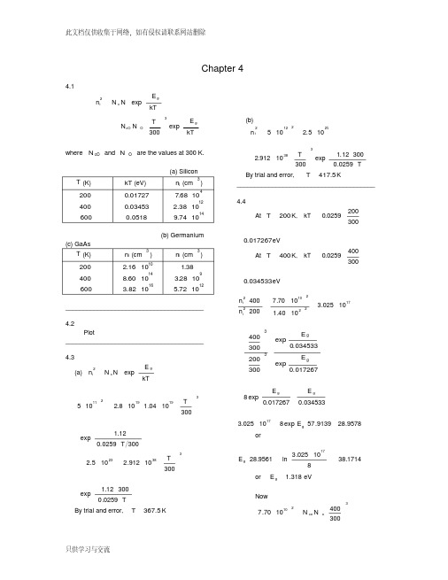
4.1
where and are the values at 300 K.
(a) Silicon
(K)
(eV)
(cm )
(b) Germanium (c) GaAs
(K)
(cm )
(cm )
_______________________________________
4.2
Plot
cm
and
cm
_______________________________________
4.39
(a) n-type
(b)
cm
cm
(c)
cm
cm
_______________________________________
4.40
cm
n-type
_______________________________________
meV
(b)
meV
_______________________________________
4.13
Let constant
Then
Let
so that
We can write
so that
The integral can then be written as
which becomes
_______________________________________
4.55
(a)Silicon
(i)
eV
(ii) eV
cm
cm Additional
donor atoms
(b)GaAs
(i)
eV
(ii) eV
cm
cm Additional
donor atoms
_______________________________________
4.56
(a)
eV
_______________________________________
4.20
(a) eV
cm
eV
cm
(b)
eV
eV
cm
_______________________________________
4.21
(a) eV
cm
eV
cm
(b)
eV
eV
cm
_______________________________________
4.7
where
and
Then
or
_______________________________________
4.8
Plot
_______________________________________
4.9
Plot
_______________________________________
4.10
4.37
(a) For the donor level
or
(b) We have
Now
or
Then
or
_______________________________________
4.38
(a) p-type
(b)Silicon:
or
cm
Then
cm
Germanium:
or
cm
Then
cm
Gallium Arsenide:
eV
eV
_______________________________________
4.16
We have
For gallium arsenide, ,
Then
The ionization energy is
or
eV
_______________________________________
4.17
4.41
cm
So cm ,
Then cm
so that cm
_______________________________________
4.42
Plot
_______________________________________
4.43
Plot
_______________________________________
we find the maximum at
_______________________________________
4.32
(a)Silicon: We have
We can write
For
eV and eV
we can write
or
cm
We also have
Again, we can write
4.36
(a)Ge: cm
(i)
or
cm
cm
(ii)
cm
cm
(b)GaAs: cm
(i) cm
cm
(ii) cm
cm
(c) The result implies that there is only one minority carrier in a volume of cm .
_______________________________________
Then
To find the maximum value:
which yields
The maximum value occurs at
nd the maximum value
Same as part (a). Maximum occurs at
or
_______________________________________
cm
(b)Boron atoms must be added
So cm
cm
_______________________________________
4.47
(a) n-type
(b)
cm
electrons are majority carriers
cm
holes are minority carriers
_______________________________________
4.3
(a)
By trial and error, K
(b)
By trial and error, K
_______________________________________
4.4
At K,
eV
At K,
eV
or
or eV
For
and eV
Then
or
cm
(b)GaAs: assume eV
Then
or
cm
Assume eV
Then
or
cm
_______________________________________
4.33
Plot
_______________________________________
4.34
_____________________________________
4.27
(a)
cm
eV
cm
(b) eV
cm
cm
eV
eV
cm
_______________________________________