19.2% efficient c-Si solar cells using ion implantation采用离子注入技术的晶硅太阳电池效率达到19.2%
二茂铁染料在敏化太阳能电池的研究进展
DOI: 10.13822/ki.hxsj.2020007577j综述与进展化学试剂,2020,42(11) ,1309〜1317二茂铁染料在敏化太阳能电池的研究进展王磊、李耀龙2,陈瑜“(1.天津理工大学,化学化工学院,天津300384;2.天津大格科技有限公司,天津301700)摘要:染料敏化太阳能电池(DSSC)已成为低成本光伏最有前途的技术之一,也是作为基于传统太阳能电池的有前途的替代品,引起了相当大的研究兴趣。
目前为止,为制作高效率的染料敏化太阳能电池,许多研究学者制作出了各种各样的敏化剂。
染料敏化剂对光收集和电子注入效率都起着至关重要的作用。
染料敏化剂可分为两种:金属有机染料敏化剂和非金属染料敏化剂。
二茂铁或二茂铁衍生物可作为供电子基的有机染料敏化剂,可以提高太阳能电池的光电转化效率,受到越来越多的关注。
关键词:有机光伏;太阳能电池;染料敏化剂;二茂铁;光电转换效率中图分类号:062丨.3 文献标识码:A文章编号:0258-3283( 2020) 11 -丨309-09Progress of Ferrocene Dyes in Sensitized Solar Cells WANG Lei' ,L I Yao-long1 ?CHEN Y u*\ 1.School of Chemistry a n d C h e mical Engineering,Tianjin University of Te c h n o l o g y,Tianjin 300384,C h i n a;2.Tianjin D a g Technology C o.,Ltd.,Tianjin 301700, C h i n a) ,H u a x u e Shiji,2020,42(11) , 1309 ~ 1317Abstract:Dye-sensitized solar cells (D S S C)have b e c o m e one of the most promising technologies for low-cost photovoltaics,and as promising alternatives to traditional solar cells,have attracted considerable research interest.So f a r,m a n y researchers have prod u c e d a variety of sensitizers to produce highly efficient dye-sensitized solar cells.Dye sensitizers play a vital role in both light collection and electron injection efficiency.There are two types of dye sensitizers :metal-organic dye sensitizers and non-metallic or- ganic dye sensitizers.Ferrocene a n d ferrocene derivatives can be used as electron-donor-based organic dye sensitizers to improve the photoelectric conversion efficiency of solar cells,which is receiving increasing attention.Key w ords:organic photochemistry;solar cells;dye sensitizers;ferrocene;photoelectric conversion efficiency随着科技的进步和人民生活水平的逐渐提高,越来越多的人开始关注国家的能源发展问题,然而随之出现的能源和燃料的危机,使得人类社会需要寻找一种可以代替化石燃料的能源。
Surface passivation of high-efficiency silicon solar cells by atomic-layer-deposited Al2O3

小学下册第十四次英语第6单元期末试卷

小学下册英语第6单元期末试卷考试时间:90分钟(总分:140)A卷一、综合题(共计100题共100分)1. 选择题:What is the smallest continent?A. AsiaB. AfricaC. AustraliaD. Europe答案:C2. 选择题:What is the term for a small rocky body that orbits the sun?A. CometB. AsteroidC. MeteorD. Planet3. 听力题:I want to ________ (create) something special.4. 选择题:What is the main purpose of a compass?A. To tell timeB. To find directionC. To measure distanceD. To calculate speed答案: B5. 填空题:The ______ (蚂蚁) works hard to gather food.6. 选择题:What is the name of the famous explorer who sailed the Pacific Ocean?A. Ferdinand MagellanB. Christopher ColumbusC. Vasco da GamaD. John Cabot答案: A7. 填空题:中国的________ (historical) 文化深深植根于传统和信仰中。
8. 选择题:What is the capital city of France?A. BerlinB. LondonC. ParisD. Madrid9. 选择题:What do we call a person who plays the piano?A. PianistB. MusicianC. ArtistD. All of the above10. 选择题:What is the name of the fairy tale character who has long hair?A. MulanB. RapunzelC. ArielD. Belle11. 填空题:The _______ (青蛙) likes to jump around.12. 选择题:What do you call a collection of books?A. LibraryB. ArchiveC. AnthologyD. Gallery答案:A13. 填空题:The _____ (小狗) is barking at the mailman.14. 听力题:The Ptolemaic model placed the Earth at the _______ of the universe.I enjoy making ______ (手工艺品) from recycled materials. It’s a fun way to be creative and eco-friendly.16. 填空题:The ancient Egyptians created vast ________ (陵墓) for their pharaohs.17. 填空题:I have a toy ______ (飞机) that can fly high in the sky. It is very ______ (酷).18. 选择题:What instrument has strings and is played with a bow?A. FluteB. PianoC. ViolinD. Drum答案: C19. 填空题:We have a ______ (特别的) day planned for school.20. 填空题:The __________ (历史的分析工具) aid in research.21. 填空题:My mom loves __________ (参加志愿活动).22. 听力题:A _______ is a reaction that releases heat.23. 选择题:What is 7 x 2?A. 12B. 14C. 16D. 18答案: B24. 听力题:The _____ (telescope) helps us see stars.25. 填空题:I enjoy watching the _______ (小动物) in the park.We are learning about _______ (动物) in school.27. 选择题:What is the name of the ocean between Africa and Australia?A. Atlantic OceanB. Indian OceanC. Arctic OceanD. Southern Ocean答案: B28. 选择题:What do you call a drink made from fermented grapes?A. BeerB. WhiskeyC. WineD. Cider答案:C29. 填空题:The ________ was a famous artist known for his paintings.30. 填空题:The __________ (历史的价值) is foundational.31. 填空题:The flamingo stands gracefully on one _________. (腿)32. 填空题:A ________ (植物景观规划) beautifies spaces.33. 填空题:The _______ (The 19th Amendment) granted women the right to vote in the US.34. 填空题:The discovery of ________ has had extensive implications for health.35. 听力题:I want to _____ (visit/see) my grandma.36. 听力题:When vinegar and baking soda mix, they produce ________.37. 填空题:The __________ (历史的讨论) can lead to greater understanding.What do you call the main character in a story?a. Antagonistb. Protagonistc. Narratord. Villain答案:B39. 填空题:My favorite subject to study is ______.40. 填空题:I want to learn how to ________ (骑车).41. 选择题:What instrument is known as the "king of instruments"?A. PianoB. OrganC. GuitarD. Violin42. 填空题:People often plant flowers for __________ (美观).43. 听力题:I like to ______ movies with my family. (watch)44. 选择题:What do we call a sweet food made from sugar and typically eaten after a meal?A. DessertB. SnackC. AppetizerD. Side dish答案:A45. 听力题:Planetary atmospheres can protect from harmful _______ radiation.46. 选择题:What do we call a story that is meant to teach a lesson?A. FableB. MythC. LegendD. Folktale答案: AThe chicken lays ______ (鸡蛋). They are a good source of ______ (蛋白质).48. 选择题:What do we call a collection of maps?A. AtlasB. DictionaryC. EncyclopediaD. Almanac答案:A49. 填空题:The __________ (历史的深度) enhances insight.50. 选择题:What do we call the person who designs buildings?A. EngineerB. ArchitectC. ContractorD. Carpenter答案: B51. 选择题:What is your name in English?A. NameB. TitleC. IdentityD. Label52. 听力题:The state of matter that fills its container is a _______.53. 选择题:Which planet is known as the Blue Planet?A. MarsB. EarthC. VenusD. Jupiter答案: B54. 听力题:The __________ can help reveal the effects of human activities on the environment.55. 听力题:The chemical formula for linoleic acid is ______.A __________ (溶胶) is a colloidal mixture with solid particles dispersed in a liquid.57. 听力题:The chemical formula for sodium acetate is _______.58. 选择题:What is the main ingredient in sushi?A. RiceB. NoodlesC. BreadD. Potatoes答案: A59. 填空题:My sister has a keen interest in __________ (天文学).60. 填空题:We saw a _______ (电影) last night.61. 选择题:What is the capital city of Nigeria?A. LagosB. AbujaC. Port HarcourtD. Kano62. 听力题:A _______ can symbolize friendship.63. 填空题:I can ______ (提升) my creativity through art.64. 选择题:What do bees make?A. MilkB. HoneyC. BreadD. Cheese答案:B65. 选择题:What do you call the act of putting something away in a safe place?A. StoringB. HidingC. KeepingD. Securing答案: A66. an Revolution led to the establishment of the ________ (苏维埃政权). 填空题:The Russ67. 填空题:I saw a _______ (小鹿) drinking water.68. 填空题:The capital of Greece is ________ (雅典).69. 填空题:The __________ (国际合作) is needed for global issues.70. 填空题:My dad enjoys helping me with ____.71. 填空题:The flamingo stands gracefully on _______ (一条腿).72. 听力题:Some birds build nests to protect their __________.73. 填空题:My brother is really _____ (幽默) and always makes me laugh.74. 选择题:How many continents are in the world?A. 5B. 6C. 7D. 875. 听力题:A __________ is a substance that cannot be broken down into simpler substances.76. 填空题:The __________ (历史的交织) creates understanding.77. 填空题:I love my _____ (毛绒玩具) that is soft.78. 听力题:The capital of Thailand is ________.79. 填空题:The __________ (历史的桥梁) connect past and present.80. 听力题:Soil is essential for ______ growth.81. 填空题:The _____ (紫罗兰) blooms in spring.82. 听力题:If you drop a feather and a rock, the rock will fall _______.83. 听力题:I want to be a ________.84. 填空题:I like to _______ new things every day.85. 选择题:How many legs does an octopus have?A. 6B. 8C. 10D. 12答案: B86. 填空题:A dolphin is a playful _______ that enjoys swimming in the sea.87. 听力题:The chemical formula for lithium hydroxide is _______.88. 填空题:I have a toy _______ that can change colors.89. 填空题:I am learning how to ________ (游泳) this summer.90. 听力题:The train is coming ___. (soon)91. 选择题:What do we call the holiday celebrated on January 1st?A. ChristmasB. New Year's DayC. Valentine's DayD. Thanksgiving92. 听力题:His favorite food is ________.93. 选择题:What do we call the force that pulls objects toward the Earth?A. MagnetismB. GravityC. FrictionD. Pressure答案:B94. 听力题:The ____ is often seen in gardens looking for food.95. 听力题:The soup is ___ (hot/cold) today.96. 填空题:__________ (植物) use water and sunlight for photosynthesis.97. 选择题:What is the main purpose of a compass?A. To measure weightB. To tell timeC. To find directionD. To measure temperature答案:C98. 填空题:A _____ (海豚) is very friendly.99. 填空题:The raccoon is known for its _______ (聪明) nature.100. 选择题:What is the capital of Estonia?a. Tallinnb. Tartuc. Narvad. Pärnu答案:a。
Solar cell--CIGS

Effect of Cu deficiency on the optical properties and electronic structure of CuInSe2 and CuIn0.8Ga0.2Se2 determined by spectroscopic ellipsometrySung-Ho Han, Allen M. Hermann, F. S. Hasoon, H. A. Al-Thani, and D. H. LeviCitation: Appl. Phys. Lett. 85, 576 (2004); doi: 10.1063/1.1776616View online: /10.1063/1.1776616View Table of Contents: /resource/1/APPLAB/v85/i4Published by the American Institute of Physics.Related ArticlesDilute-nitride GaInAsN/GaAs site-controlled pyramidal quantum dotsAppl. Phys. Lett. 99, 181113 (2011)Modifications in structural and electronic properties of TiO2 thin films using swift heavy ion irradiation J. Appl. Phys. 110, 083718 (2011)Point defects in gallium nitride: X-ray absorption measurements and multiple scattering simulations Appl. Phys. Lett. 99, 172107 (2011)Spontaneous polarization and band gap bowing in YxAlyGa1-x-yN alloys lattice-matched to GaNJ. Appl. Phys. 110, 074114 (2011)Band gap and electronic properties of wurtzite-structure ZnO co-doped with IIA and IIIAJ. Appl. Phys. 110, 063724 (2011)Additional information on Appl. Phys. Lett.Journal Homepage: /Journal Information: /about/about_the_journalTop downloads: /features/most_downloadedInformation for Authors: /authorsEffect of Cu deficiency on the optical properties and electronic structure of CuInSe2and CuIn0.8Ga0.2Se2determined by spectroscopic ellipsometry Sung-Ho Han a)and Allen M.HermannDepartment of Physics,University of Colorado,Boulder,Colorado80303-0390F.S.Hasoon,H.A.Al-Thani,and D.H.LeviNational Renewable Energy Laboratory,1617Cole Boulevard,Golden,Colorado80401-3393(Received29March2004;accepted4June2004)Spectroscopic ellipsometry measurements of CuInSe2(CIS)and CuIn0.8Ga0.2Se2(CIGS)reveal thatthere are important differences in electronic properties between stoichiometric CIS(CIGS)andCu-poor CIS(CIGS).Wefind a reduction in the absorption strength in the spectral region of1–3eV.This reduction can be explained in terms of the Cu3d density of states.Cu-poor CIS(CIGS)materials show an increase in band gap due to the reduction in repulsion between Cu3d andSe4p states.The experimental results have important implications for the function ofpolycrystalline optoelectronic devices.©2004American Institute of Physics.[DOI:10.1063/1.1776616]Polycrystalline thin-film chalcopyrite CuIn1−x Ga x Se2 (CIGS)is currently used as an absorber layer for high-efficiency photovoltaic(PV)solar cells.The efficiency of record laboratory polycrystalline thin-film solar cells based on CIGS has reached nearly20%,1while single-crystalline CIGS solar cells have just reached13%.2Electronic struc-tures of CuB III X2VI materials have been thoroughly studied.3–5 High-efficiency polycrystalline solar cells are always slightly Cu deficient,with about23.5–24.5at.%Cu.There have been studies of the optical properties of CIGS materials with different Ga compositions,6–8but considering the fact that high-efficiency PV solar cells use Cu-poor CIGS,it is crucial to study the effect of content on CIGS electronic properties. In this study,through the analysis of the dielectric function, we compare the electronic structure of Cu-poor ͑21.7at.%Cu͒CuInSe2(CIS)films with stoichemetric ͑25.1at.%Cu͒CISfilms.We also compare the electronic structure of slightly Cu-poor͑23.3at.%Cu͒CIGSfilms withstoichiometric͑24.8at.%Cu͒bulk polycrystalline CIGS.CIGS surfaces are inclined to have Cu vacancies.9,10In con-trast to zinc-blende semiconductors,where the nonpolar (110)surface is more stable than all polar surfaces,the chal-copyrite semiconductor CuInSe2has the lowest energy when the surface has the(112)-cation and͑1¯1¯2¯͒-anion polar facets through defect-induced reconstructions.9Previous work has studied electronic and geometric structures of nearly sto-ichiometric bulk and Cu-poor surfaces.4,10,11In contrast,we focus on Cu-poor CIS and CIGS samples where both the surface and bulk regions are Cu poor to probe the properties of Cu-deficient CIS(CIGS)materials.Spectroscopic ellipsometry(SE)is a powerful technique for determining the optical functions of bulk and thin-film materials.Alonso et al.have reported SE measurements of the pseudodielectric functions of single-crystalline CIS and CuGaSe2(CGS),6as well as bulk polycrystalline CIGS alloys.7In those studies,they used a two-phase model to analyze the ellipsometric data.12Such a treatment is not ap-propriate for the analysis of thin-film polycrystalline materi-als used for real-world CIGS solar cells.The polycrystalline thin-film CIS and CIGS samples were deposited onto molybdenum-coated soda-lime glass.The molybdenum thickness was about1.0m.CIS and CIGS layer thick-nesses were about1.2m and2.0m,respectively.These films were grown by the single-stage coevaporation tech-nique,where thefluxes of Cu,In,Ga,and Se were constant during deposition.To accurately determine the optical prop-erties of these multilayer thin-film samples,one must analyze the SE data using a full multilayer model including the ef-fects of the surface roughness and the underlying molybde-num layer.8We have applied these techniques to determine the dielectric functions for several polycrystalline thinfilms of CIS and CIGS alloys.The ellipsometer used to make the measurements in this study is a J.A.Woollam M2000variable-angle spectroscopic ellipsometer,which uses a rotating compensator design.For this work,ellipsometric spectra were measured at angles of incidence of65°,70°,75°,and80°to ensure an accurate determination of the dielectric function of the material,the thicknesses of the material layer,and surface roughness layer.Auger electron spectroscopy(AES)depth profiles showed that the materials have uniform compositions throughout the entire thickness of thefilms.Thicknesses measured by profilometer are in quantitative agreement with those determined by SE.Inductively coupled plasma(ICP) analysis measures the compositions of thin-film CIS and CIGS.Table I provides at.%Cu of thesefilms as determineda)Also with:National Renewable Energy Laboratory,Golden,CO80401; electronic mail:sung-ho.han@ TABLE I.at.%Cu and critical points analyzed by the CPPB model.All samples are polycrytalline.Stoichiometricthin-film CISCu-poorthin-film CISStoichiometricbulk CIGS aSlightlyCu-poorthin-film CIGS at.%Cu25.121.724.823.3E0͑A,B͒ 1.03 1.08 1.11 1.12E0͑C͒ 1.22 1.29 1.33 1.34a Ref.7.APPLIED PHYSICS LETTERS VOLUME85,NUMBER426JULY2004 0003-6951/2004/85(4)/576/3/$20.00©2004American Institute of Physics576by ICP.X-ray diffraction revealed that these films are single phase for stoichemetric thin-film CIS ͑25.1at.%Cu ͒and slightly Cu-poor ͑23.3at.%Cu ͒thin-film CIGS,and mixed phase for Cu-poor ͑21.7at.%Cu ͒thin-film CIS.The CuIn 0.8Ga 0.2Se 2material studied by Alonso et al.also showed uniform chalcopyrite structure with no secondary phases found.7More detailed discussion on the experimental conditions can be found in Ref.8.Figure 1(a )compares the absorption coefficient spectra of stoichemetric and Cu-poor CIS.Figure 1(b )extends this comparison to CIGS materials to generalize the effect of Cu on CIGS materials.Both Figs.1(a )and 1(b )show similar trends.Relative to the stoichiometric samples,absorption de-creases in E 0,E ͑⌫X ͒,and E 1͑A ͒transitions,but increases in the E ͑⌬X ͒transition for Cu-poor materials.The optical tran-sitions in the spectral range of 1–5eV,can be found else-where .6,7Depression of the absorption coefficient is found in Fig.1(a )between stoichiometric ͑24.8at.%Cu ͒thin-film CIS and Cu-poor ͑21.7at.%Cu ͒thin-film CIS in the spec-tral region,1–3eV.Although the band-gap energies are slightly different due to different Ga compositions,Fig.1(b )also shows the depression of absorption coefficient between stoichiometric bulk polycrystalline CuIn 0.8Ga 0.2Se 2and slightly Cu-poor thin-film CIGS with x ϵGa/͑In+Ga ͒=0.18.According to the theoretical calculations of the elec-tronic band structure and density of state (DOS )of the ter-nary chalcopyrite materials by Jaffe and Zunger,3the upper valence band,within 3–4eV of the valence-band maximum (VBM ),is composed primarily of the Cu 3d orbitals,hybrid-ized with the Se-4p orbitals.Several authors have calculated the band structure and DOS of extremely Cu-poor ␥-phase CIS ͑CuIn 5Se 8͒.5Both of these calculations show a reduction of the DOS within 3–4eV of the VBM.Reduction in the DOS of hole states near the VBM should produce a decrease in absorption coefficient near the band edge.This theoretical result is consistent with our experimental observations.Theoretical calculations of CIS band structure predict another effect of Cu deficiency.As stated above,in ternary chalcopyrite CuB III X 2VI ,the upper valence band is composed of Cu 3d and VI 4p state electrons.This was observed ex-perimentally using synchrotron radiation photoemission spectroscopy.13The repulsive p –d interaction pushes the an-tibonding p –d state that constitutes the VBM to higher en-ergies.In the case of Cu-poor CIS and CIGS,the p –d repul-sion is expected to be less than that of stoichiometric materials.The net effect of the decrease in this repulsive interaction would then be a lowering of the VBM.Hence,we expect an increase of the band gap for Cu-poor CIGS.14We analyze the band gap using the critical-point para-bolic band (CPPB )model.14The fitting procedure is done on the calculated second derivative of dielectric function d 2͑͒/d 2,using the method of smoothing polynomials 15to enhance the structure present in the spectra.The structure of the fundamental absorption edge of CuInSe 2is well known.3Considering crystal-field splitting and spin–orbit in-teraction,the three-fold degenerate ⌫15VBM splits into three transitions E 0͑A ͒,E 0͑B ͒,and E 0͑C ͒.The measured critical points are compiled in Table I.In the case of CIS and CuIn 0.8Ga 0.2Se 2,the separation between E 0͑A ͒and E 0͑B ͒cannot be measured because it is below our resolution.7Thus,the structure is composed of the two degenerate peaks,E 0͑A ,B ͒and E 0͑C ͒.E 0͑A ,B ͒and E 0͑C ͒of stoichemetric thin-film CIS 1.03eV and 1.22eV and those of Cu-poor thin-film CIS are 1.08eV and 1.29eV,respectively.We can see that the band gap increases by 0.05eV for Cu-poor CIS.CPs of CIGS materials show trends analogous to those of CIS materials.We compare the dielectric function of bulk polycrystalline stoichiometric ͑24.8at.%Cu ͒CuIn 0.8Ga 0.2Se 2from Alonso et al.7with the dielectric func-tion of slightly Cu-poor ͑23.3at.%Cu ͒thin-film CIGS with x =0.18.E 0͑A ,B ͒,and E 0͑C ͒of bulk stoichiometric CIGS are extracted from the equation with x =0.18in Alonso et al.7According to that calculation,E 0͑A ,B ͒,and E 0͑C ͒of sto-ichiometric bulk CIGS are 1.11eV and 1.33eV,whereas E 0͑A ,B ͒and E 0͑C ͒of slightly Cu-poor thin-film CIGS are 1.12eV and 1.34eV,respectively.We can see that the band gap increases by 0.01eV.This value is smaller than that of CIS due to the smaller difference in the quantities of at.%Cu.Considering our experimental results in the context of the theoretical calculations of the band structure of stoichio-metric and Cu-poor CIS (CIGS ),3–5we have shown that the reduction of the near band-edge absorption coefficient ob-served in Cu-poor CIS (CIGS )is related to a decrease in the density of states near the VBM.This result has important implications for the functioning of high-efficiencypolycrys-FIG.1.(a )Comparison of absorption coefficients between stoichiometric ͑25.1at.%Cu ͒thin-film CIS and Cu-poor thin-film CIS ͑21.7at.%Cu ͒(b ).Comparison of absorption coefficients between stoichiometric ͑24.8at.%Cu ͒bulk polycrystalline CIGS with x =0.2by Alonso et al.(Ref.7)and slightly Cu poor ͑23.3at.%Cu ͒with x =0.18.talline CIGS thin-film the highest.As stated previously,high-est efficiency CIGS PV devices are slightly Cu poor,with23.5–24.5at.%Cu.Theoretical calculations have shown thatthe most energetically favorable surfaces for CIS are the (112)-cation and͑1¯1¯2¯͒-anion polar facets with defect-induced reconstructions producing a layer of Cu vacancies atthe surface.9Numerous experimental measurements haveconfirmed that CIS(CIGS)surfaces are Cu poor.10Becausegrain boundaries(GBs)can be considered as interior sur-faces,it is reasonable to postulate that in the slightly Cu-poorCIGS material used in high-efficiency solar cells,the mate-rial near the GBs is Cu poor,while the grain interiors(GIs)are nearly stoichiometric.4As shown in Ref.4,the reductionof the DOS near the VBM at the GBs effectively produces acharge-neutral barrier to holes.This effectively passivatesthe GBs by only allowing minority-carrier electrons to pen-etrate the GB region.It is known that the GBs act to getterthe defects and impurities in these materials;hence,passiva-tion of the GBs is exceptionally effective in reducing nonra-diative recombination in CIS(CIGS)thin-film solar cells.The Cu-poor materials studied in this letter are significantly more Cu deficient than the materials used in solar cells.It is reasonable to assume that both GIs and GBs are Cu poor in thesefilms.Hence,our measurements of the optical proper-ties and electronic structure reveal the properties of the GB material in an actual solar cell.Hence,these experimental measurements serve as a confirmation of the theoretical cal-culations put forth in Ref.4.The authors thank H.Moutinho for assistance in atomic force microscopy measurements,R.Bhattacharya for assis-tance in ICP measurements,and J.Pankow for assistance in AES profile measurements.The authors acknowledge valu-able discussions with R.Noufiand C.Persson.This work was supported by the U.S.Department of Energy under Con-tract No.DE-AC36-99GO10337.1K.Ramanathan,M.A.Contreras,C.L.Perkins,S.Asher,F.S.Hasoon,J. Keane,D.Young,M.Romero,W.Metzger,R.Noufi,J.Ward,and A. Duda,Prog.Photovoltaics11,225(2003).2C.H.Champness,Proceedings of the29th IEEE Conference(IEEE,Pis-cataway,NJ,2002),p.732;L.S.Yip and I.Shih,Proceedings of the First World Conference on Photovoltaic Energy Conversion(IEEE,Piscataway, NJ,1994),p.210.3J.E.Jaffe and A.Zunger,Phys.Rev.B27,5176(1983);ibid.28,5822 (1983);ibid.29,1882(1984).4C.Persson and A.Zunger,Phys.Rev.Lett.91,266401(2003).5S.B.Zhang,S.-H.Wei,and A.Zunger,Phys.Rev.B57,9642(1998);C. Domain,ribi,S.Taunier,and J.F.Guillemoles,J.Phys.Chem.Solids 64,1657(2003).6M.I.Alonso,K.Wakita,J.Pascual,M.Garriga,and N.Yamamoto,Phys. Rev.B63,075203(2001).7M.I.Alonso,M.Garriga,C.A.Durante Rincön,E.Hernández,and M. León,Appl.Phys.A:Mater.Sci.Process.74,659(2002).8S.-H.Han,D.H.Levi,H.A.Al-Thani,F.S.Hasoon,R.N.Bhattacharya, and A.M.Hermann,Mater.Res.Soc.Symp.Proc.763,B1.8(2003).9J.E.Jaffe and A.Zunger,Phys.Rev.B64,241304(2001);S.B.Zhang and S.-H.Wei,ibid.65,081402(2002);J.E.Jaffe and A.Zunger,J.Phys. Chem.Solids64,1547(2003).10R.Herberholz,U.Rau,H.W.Schock,T.Haalboom,T.Gödecke,F.Ernst, C.Beilharz,K.W.Benz,and D.Cahen,Eur.Phys.J.:Appl.Phys.6,131 (1999);D.Liao and A.Rockett,Appl.Phys.Lett.82,2829(2003).11A.Meeder,L.Weinhardt,R.Stresing,D.Fuertes Marrón,R.Würz,S.M. Babu,T.Schedel-Niedring,M.C.Lux-Steiner,C.Heske,and E.Umbach, J.Phys.Chem.Solids64,1553(2003);I.M.Kötschau and H.W.Schock, ibid.64,1559(2003);J.M.Merino,M.Di Michiel,and M.León,ibid. 64,1649(2003).12R.M.A.Azzam and N.M.Bashara,Ellipsometry and Polarized Light (North-Holland,Amsterdam,1977).13M.Turowski,G.Magaritondo,M.K.Kelly,and R.D.Tomlinson,Phys. Rev.B31,1022(1985).utenschlager,M.Garriga,S.Logothetidis,and M.Cardona,Phys. Rev.B35,9174(1987).15A.Savitzky and M.J.E.Golay,Anal.Chem.36,1627(1964);J.Steinier, Y.Termonia,and J.Deltour,Anal.Chem.44,1906(1972).。
小学上册第十四次英语上册试卷(含答案)
小学上册英语上册试卷(含答案)英语试题一、综合题(本题有50小题,每小题1分,共100分.每小题不选、错误,均不给分)1 The _____ (teacher/student) is helpful.2 A ______ is a small creature that can be found in ponds.3 The _____ (园艺技巧) can enhance your gardening skills.4 What is the main language spoken in the USA?A. SpanishB. FrenchC. EnglishD. German5 The _____ (balloon/kite) is flying.6 The _______ of a swing is caused by gravity.7 What is 14 + 6?A. 18B. 19C. 20D. 21答案:A8 Abraham Lincoln delivered the Gettysburg __________ (演讲) during the Civil War.9 There are ___ (three/four) books on the table.10 How many strings does a violin have?A. 4B. 5C. 6D. 711 What is the name of the famous ancient structure in England?A. StonehengeB. ColosseumC. Great WallD. Pyramids答案: A. Stonehenge12 What do you call a journey to space?a. Explorationb. Expeditionc. Flightd. Mission答案:D13 This ________ (玩具) is full of possibilities.14 In summer, I enjoy _______ (游泳) in the pool.15 What do we call a large body of saltwater?A. OceanB. SeaC. GulfD. Bay答案: A16 What do we call the tool we use to measure temperature?A. ThermometerB. BarometerC. HydrometerD. Anemometer17 I can see a __________ in the sky.18 I like swimming in the _____ (pool/desk).19 We will go to the ______ (museum) on Saturday.20 We have a ______ (愉快的) celebration for achievements.21 What is the name of the famous mouse created by Walt Disney?A. Mickey MouseB. Donald DuckC. GoofyD. Pluto22 I want to _____ (see/watch) a movie tonight.23 My favorite animal is a ______ (狗) because they are loyal.24 _____ (农田) are areas where crops are grown.25 Salt dissolves in _____.26 How many colors are in a rainbow?A. FiveB. SixC. SevenD. Eight27 The chemical formula for glucose is ______.28 What does a light-year measure?B. DistanceC. SpeedD. Mass29 Which season comes after spring?a. Winterb. Summerc. Falld. Autumn答案:b30 The _____ (冬季) can be harsh for some plants.31 The peacock has beautiful _________. (羽毛)32 The chemical industry produces a wide range of ________ for various applications.33 The soup is ______ (warm) and delicious.34 The dog is _______ (running) after the ball.35 The __________ (历史的呼唤) resonates deeply.36 What is the name of the famous river in Egypt?A. NileB. AmazonC. MississippiD. Yangtze答案: A37 What do we call a place where we can see art?A. MuseumB. GalleryD. Workshop38 Pulsars are rotating neutron _______ that emit beams of radiation.39 The main component of starch is ______.40 The ancient Greeks constructed ________ for their religious ceremonies.41 What is the opposite of "happy"?A. JoyfulB. SadC. ExcitedD. Cheerful42 The ________ (农业可持续发展目标) guide practices.43 The _______ of sound can be amplified with a speaker.44 The ________ (feedback) helps us improve.45 What is the name of the first satellite sent into space?A. Apollo 11B. SputnikC. Voyager 1D. Hubble46 What is the name of the famous American landmark in New York City?A. Golden Gate BridgeB. Statue of LibertyC. Empire State BuildingD. Mount Rushmore47 A dwarf planet is similar to a planet but does not clear its orbit of ______.48 What is the term for an animal that eats both plants and meat?A. HerbivoreB. CarnivoreC. OmnivoreD. Insectivore答案:C. Omnivore49 My brother is my silly _______ who always knows how to make me smile.50 The __________ is a large area of sandy soil.51 What is the name of the famous bear in the cartoon?A. PaddingtonB. Winnie the PoohC. YogiD. Baloo答案:B52 What is the capital of Portugal?A. LisbonB. PortoC. FaroD. Braga53 The study of rocks is known as ______.54 What is the name of the device used to measure pressure?a. Barometerb. Hygrometerc. Thermometerd. Anemometer答案:a55 The __________ (历史的抉择) shapes destiny.56 The __________ is known for its unique wildlife and natural beauty. (新西兰)57 The chemical formula for acetylene is ______.58 Which of these is a cold-blooded animal?A. HumanB. SharkC. SnakeD. Bird答案:C59 I like to _____ (collect/throw) stamps.60 I want to grow a ________ to make my room bright.61 Which animal is known as "man's best friend"?A. CatB. DogC. RabbitD. Fish答案:B62 The _______ (小驴) brays loudly in the pasture.63 My favorite animal at the zoo is a ________.64 The __________ (历史的探索者) uncover stories long forgotten.65 What is the main ingredient in a smoothie?A. IceB. MilkC. FruitD. Sugar66 What is the name of the fairy tale character with long hair?A. CinderellaB. RapunzelC. Snow WhiteD. Belle67 What do we call the solid part of the Earth?A. AtmosphereB. HydrosphereC. LithosphereD. Biosphere答案:C68 I need to _____ (finish/start) my homework.69 What is the name of the large body of saltwater that covers most of the Earth?A. LakeB. SeaC. OceanD. River答案:C70 A cheetah is the fastest _______ on land, running swiftly to catch its prey.71 What do we call a scientist who studies the effects of pollution?a. Environmental scientistb. Ecologistc. Biologistd. Chemist答案:a72 What is the name of the ocean located between Africa and Australia?A. Indian OceanB. Atlantic OceanC. Pacific OceanD. Arctic Ocean答案:A73 The ______ (植物分类) helps identify species.74 The basic unit of a protein is an ________.75 What do you call a young ant?A. LarvaB. PupaC. WorkerD. Queen76 The chemical properties of a substance are observed during a _____ change.77 The first man on the moon was ________ (尼尔·阿姆斯特朗).78 My favorite subject is __________. (数学)79 A garden can attract various ______ (昆虫).80 What is the capital of Cyprus?A. NicosiaB. LimassolC. LarnacaD. Famagusta答案:A81 What do we call the sound a sheep makes?A. MooB. QuackC. BaaD. Neigh答案:C82 I can ________ (jump) very high.83 I like to draw _____ in my notebook.84 My brother has a great sense of __________ (幽默感).85 What do we call the traditional game played with a ball and net?A. CricketB. BaseballC. TennisD. Soccer86 The ____ is known for its agility and speed.87 What do you call a place where animals are kept for public display?A. ParkB. ZooC. FarmD. Aquarium答案: B88 My cousin is very __________ (活泼的) and energetic.89 What is the name of the famous artist known for his paintings of water lilies?A. Claude MonetB. Vincent van GoghC. Pablo PicassoD. Salvador Dalí90 What do we call a young female horse?A. FillyB. ColtC. FoalD. Mare91 What do you call a person who swims?A. DiverB. SurferC. SwimmerD. Sailor答案:C92 What do you call the liquid that comes from trees?A. GumB. SyrupC. SapD. Juice答案:C93 What is the capital of Australia?A. SydneyB. CanberraC. MelbourneD. Brisbane94 A fuel is a substance that can be burned to produce _____.95 The __________ is heavy with clouds. (天空)96 What is the smallest unit of life?A. TissueB. OrganC. CellD. Organism97 The study of compounds containing carbon is called ______ chemistry.98 The process of making charcoal involves _______.99 The __________ is known for its diverse ecosystems.100 We enjoy _____ to the library. (going)。
高一英语生物词汇单选题30题
高一英语生物词汇单选题30题1.The basic unit of life is the_____.A.atomB.moleculeC.cellD.tissue答案:C。
“atom”是原子;“molecule”是分子;“cell”是细胞,生命的基本单位是细胞;“tissue”是组织。
2.Which structure is responsible for controlling what enters and leaves the cell?A.nucleusB.cell membraneC.cytoplasmD.chloroplast答案:B。
“nucleus”是细胞核;“cell membrane”是细胞膜,负责控制物质进出细胞;“cytoplasm”是细胞质;“chloroplast”是叶绿体。
3.The power house of the cell is_____.A.nucleusB.mitochondrionC.endoplasmic reticulumD.Golgi apparatus答案:B。
“nucleus”是细胞核;“mitochondrion”是线粒体,被称为细胞的动力工厂;“endoplasmic reticulum”是内质网;“Golgi apparatus”是高尔基体。
4.Which organelle is involved in protein synthesis?A.ribosomeB.lysosomeC.vacuoleD.peroxisome答案:A。
“ribosome”是核糖体,参与蛋白质合成;“lysosome”是溶酶体;“vacuole”是液泡;“peroxisome”是过氧化物酶体。
5.The storage site of genetic information is the_____.A.nucleusB.mitochondrionC.chloroplastD.cytoplasm答案:A。
基质血管组分(SVF)临床分离技术研究
中国细胞生物学学报 Chinese Journal of Cell Biology2021,43( 1):73-82 DOI: 10.11844/cjcb.2021.01.0010基质血管组分(SVF)临床分离技术研究李智国张方方刘悦刘建兴金亮*(中国药科大学,南京211100)摘要 脂肪组织易获取、组织相容性好且对供体影响小,可作为获得成体干细胞的重要来源。
基质血管组分(S V F)是从脂肪中分离出来的包括脂源性干细胞(A D S C)和基质细胞的异质性细 胞群。
S V F促进组织的修复和再生已被大量的临床实验所证实,尤其是在美容整形和组织修复中的应用。
早期,S V F通过酶消化法获得,随着近年来在临床中扩大应用,为确保患者安全和质量可控,开发出新型自动分离设备。
同时,为符合一些国家监管要求,避免酶的使用,采用非酶消化法获取 S V F。
因此,该文主要针对基于酶消化法和非酶消化法已经发表临床分离方法和上市的相关设备 作详细论述。
关键词基质血管组分;酶消化法;非酶消化法;分离设备;The Research of Clinical Separation of SVF (Stromal Vascular Fraction)LI Zhiguo,Z H A N G Fangfang,L I U Y u e,L I U Jianxing,JIN Liang*{China Pharmaceutical University, Nanjing 211100, China)Abstract Adipose tissue is an important source of stem cells because i t is easy to access and has a g o o d histocompatibility and l i t t l e influence on donors.S V F(stromal vascular fraction)is a heterogeneous group of cells isolated from adipose tissue,including A D S C(adipose derived stem cell)and stromal cells.According to a large n u m b e r of clinical trials,S V F has been proved that i t can promote tissue to repair and regenerate,especially in cosmetic surgery and tissue repair.In the early stage,S V F w a s obtained by e n z y m e digestion.With the extensive application of S V F in clinical practice during recent years,in order to ensure patient safety and quality control,s o m e n e w automatic separation equipment w a s developed.M e a n w h i l e,in order to meet the regulatory requirements of s o m e countries and avoid the use of e n z y m e,non-enzymatic digestion m e t h o d b e c o m e s a w a y of obtaining S V F. Therefore,current essay i s primary to m a k e a detailed discuss about reported clinical separation w a y s a nd related equipments based on the e n z y m e digestion and non-enzyme digestion.K e y w o r d s stromal vascular fraction;enzymatic digestion;non-enzymatic digestion;separation equipmentI960年,R O D B E L L l[11首次将大鼠脂肪通过胶 原酶消化,离心后脂肪分成三个不同密度层,最下 层为颗粒层,该层包含多种细胞群体。
perovskite solar cells

Nanophotonic front electrodes for perovskite solar cellsUlrich Wilhelm Paetzold, Weiming Qiu, Friedhelm Finger, Jef Poortmans, and David CheynsCitation: Applied Physics Letters 106, 173101 (2015); doi: 10.1063/1.4918751View online: /10.1063/1.4918751View Table of Contents: /content/aip/journal/apl/106/17?ver=pdfcovPublished by the AIP PublishingArticles you may be interested inLight trapping in thin-film solar cells via scattering by nanostructured antireflection coatingsJ. Appl. Phys. 114, 044310 (2013); 10.1063/1.4816782Influence of the pattern shape on the efficiency of front-side periodically patterned ultrathin crystalline silicon solar cellsJ. Appl. Phys. 112, 113107 (2012); 10.1063/1.4768529Metallic nanomesh electrodes with controllable optical properties for organic solar cellsAppl. Phys. Lett. 100, 143109 (2012); 10.1063/1.3701582Liquid transfer imprint lithography: A new route to residual layer thickness controlJ. Vac. Sci. Technol. B 29, 06FC12 (2011); 10.1116/1.3660792Micromorph thin-film silicon solar cells with transparent high-mobility hydrogenated indium oxide front electrodes J. Appl. Phys. 109, 114501 (2011); 10.1063/1.3592885Nanophotonic front electrodes for perovskite solar cellsUlrich Wilhelm Paetzold,1,2,a)Weiming Qiu,1Friedhelm Finger,2Jef Poortmans,1,3,4and David Cheyns 11IMEC v.z.w.,Kapeldreef 75,3001Leuven,Belgium2IEK5-Photovoltaik,Forschungszentrum Juelich GmbH,D-52425Juelich,Germany 3Katholieke Universiteit Leuven,ESAT-Electa,Kardinaal Mercierlaan,3001Leuven,Belgium 4Hasselt University,Wetenschapspark 1,3590Diepenbeek,Belgium(Received 5February 2015;accepted 10April 2015;published online 27April 2015)In less than 3years’time,a vast progress in power conversion efficiencies of organometal halide perovskite solar cells has been achieved by optimization of the device architecture,charge transport layers,and interfaces.A further increase in these efficiencies is expected from an improvement in the optical properties via anti-reflection coatings and nanophotonic light management concepts.In this contribution,we report on the development and implementation of a nanophotonic front electrode for perovskite solar cells.The nanostructures were replicated via the versatile and large-area compatible UV-nanoimprint lithography.The shallow design of the used transparent and conductive nanostructures enabled easy integration into our solution-based baseline process.Prototype methylammonium lead iodide perovskite solar cells show an improvement of 5%in short-circuit current density and an improvement from 9.6%to 9.9%in power conversionefficiency compared to the flat reference device.VC 2015AIP Publishing LLC .[/10.1063/1.4918751]The enormous potential and recent vast development of organometal halide perovskite solar cells has triggered an unprecedented fast progress of its power conversion efficien-cies (g ).Today,less than 3years after the first reported solid state perovskite solar cell 1a record efficiency of 20.1%2has been certified and several groups have reported efficiencies above 17%.3,4The current key challenges of perovskite solar cells are the apparent uncertainties about the stability of the devices,5–7the discrepancies in measuring routines due to hysteresis,8,9and the difficulties in replacing the toxic heavy metal lead.10,11The promise of perovskite solar cells is founded in their close to optimal combination of electrical and optical material properties.Free carrier diffusion lengths from 100nm (Refs.12and 13)up to 1l m (Ref.13)have been reported for the current work-horse materials,methyl-ammonium lead iodide perovskite (CH 3NH 3PbI 3)and the partially chlorine-substituted mixed halide perovskite (CH 3NH 3PbI 3ÀX Cl X ).In addition,the material shows a sharp optical absorption edge at wavelengths of 800nm (i.e.,1.55eV)with absorption depths below 350nm (for k <750nm).14Since the combination of these material properties allows for optically thick layers (!350nm)in combination with close to optimal charge carrier collection,the first attention in the development of perovskite solar cells was directed towards the optimization 3,15–18of the charge carriers dynamics in the device architecture,3,7,13,15–23in the charge transport layers,12,24,25and in the interfaces.4,26However,in order to further improve the efficiencies,the optical aspects of organometal halide perovskite solar cells need optimization.The reflection at the air/substrate inter-face is around 4%and additional reflection and parasitic absorption losses are apparent at the transparent frontcontact.While a broad range of anti-reflection coatings for the front side of transparent glass and plastic substrates have been explored,27research on nanophotonic transparent front electrodes for perovskite solar cells for improved light incou-pling is lacking.Such nanostructured electrodes areintendedFIG.1.Nanophotonic ITO front electrodes for application in perovskite thin-film solar cells.(a)A photograph of the ITO front electrode on the glass substrate.The colored haze depicts the light diffraction of the nanopatterned regions of the electrode.Scanning electron microscopy (SEM)image of the surface topography of the nanopatterned ITO front electrode with a period of (b)500nm and (c)1000nm.a)Author to whom correspondence should be addressed.Electronic mail:ulrich.w.paetzold.ext@imec.be0003-6951/2015/106(17)/173101/5/$30.00VC 2015AIP Publishing LLC 106,173101-1APPLIED PHYSICS LETTERS 106,173101(2015)to reduce reflection at both interfaces of the front electrode. Moreover,they can be used to improve the light-trapping, i.e.,increase the optical path length in the photo-active material.Such nanophotonic transparent front electrodes have already been researched and prototyped for a number of other solar cells,such as organic based PV,28–30 thin-film silicon,31,32GaAs(Ref.33),and crystalline silicon.34,35In this contribution,we report on the prototyp-ing and application of transparent nanophotonic front elec-trodes for improved light incoupling in perovskite solar cells.The nanophotonic front electrode was prepared by nano-patterning a transparent glass-like resist on a plane glass sub-strate(3Â3cm2).With a soft-polymer mold and a UV-nanoimprint process,periodic nanopatterns were transferred into the transparent resist that hardens at intense UV expo-sure(details on the nanoimprint process are described in the supplemental material36well as the literature37,38).A125nm thick indium-tin-oxide(ITO)layer was then sputtered onto the resist,forming the front electrode.The nanopatterned regions exhibit areas of0.5Â0.5cm2and periods ranging from1200nm to500nm.In contrast to theflat reference, light diffraction at periodic nanopatterns causes spectral selective redirection of light that can be observed by eye (shown in Figure1(a)).Due to the moderate conformal growth of the sputtered ITO,the rectangular nanostructures at the surface of the UV-nanoimprinted resist(80nm height and300nm width)reveal a semi-ellipsoidal shape(around 80nm height and320nm width)at the ITO surface(see Figures1(b)and1(c)).A methylammonium lead iodide perovskite solar cell was fabricated on top of the ITO front electrode.Since our substrate holds both nanopatterned andflat regions,it was possible to process both nanopatterned and reference devices in parallel and on the same substrate,i.e.,using the same sputtered ITO material quality and layer thickness.36 Moreover,our experiments ensure optimal comparability of the device architecture and material compositions,which is otherwise difficult to achieve for solution-processed layers. In Figure2(a),a photograph of the entire device is shown. Five areas of0.5Â0.5cm2with decreasing brightness indi-cate the regions of the nanopatterns at the ITO front elec-trode.Some of the nanopatterns show a colored haze due to light diffraction at the two-dimensional nanopattern of the front electrode.The solar cells layer sequence was deposited onto these electrodes in the conventional device architecture, with the hole transport layer at the front electrode and the electron transport layer at the Al back electrode(layer sequence in Figure2(b)).The device architecture presented here has been proposed before in literature by Bai et al.39A FIG.2.Prototype methylammonium lead iodide solar cell.(a)A photography of the substrate from the front side.Thefive areas with decreased brightness indicate the regions of the nanopatterns of the ITO front electrode.For the500,600,and800nm patterns,light diffraction is apparent by a colored haze.(b)A schematic illustration of the nanopatterned perovskite solar cell.(c)Images of atomic force microscopy measurements of the nanopatterned resist,the nanopat-terned resist covered with ITO,and the rear side of the perovskite solar cell.(d)The absorptance A and(e)the external quantum efficiency EQE of the methyl-ammonium lead iodide solar cells with nanophotonic electrodes compared to solar cells deposited on theflat reference electrode.The period of the nanopattern is varied from500nm to1200nm.spin-coated poly(3,4-ethylenedioxythiophene):poly(4-styre-nesulfonate)(PEDOT:PSS)layer acts as hole transport layer in contact with the ITO front electrode.The photoactive methylammonium lead iodide perovskite CH3NH3PbI3Cl layer was prepared by annealing a“pristine”spin-coated precursor solution(CH3NH3PbI3ÀX Cl X).A spin-coated [6,6]-phenyl C60-butyric acid methyl ester(PC60BM)and a spin-coated zinc oxide establish the bilayer-structured elec-tron transporting layer.Finally,the reflective Al back elec-trode was deposited through a shadow mask defining the cell area(approximately15mm2).More details on the processing conditions and composition of the applied solutions are pre-sented in the supplemental material.36The thickness of the perovskite absorber layer was determined by profilometer measurements to320nm.The conformity of the ITO deposi-tion on the nanopatterned substrates was investigated with atomic force microscopy measurements(Figure2(c)).It is shown that the front electrode is nanostructured but the back electrode isflat.Since the photoactive perovskite layer is significantly thicker than the nanostructure at the front elec-trode,the nanopattern is not apparent at the back electrode. The combination of PC60BM and ZnO layers is of particular importance to our device architecture.This double layered electron transport structurefills the cavities existing in the methylammonium lead iodide perovskite layer after forma-tion of the crystallites,while a low resistive contact with the cathode is attained with the ZnO.The photograph in Figure2(a)reveals that absorptance of incident light is increased for the solar cells deposited on the nanopatterned front electrodes compared to theflat reference.In order to quantify this observation we show the spectral resolved absorptance of the solar cells deposited on the nanophotonic front electrodes with periods ranging from 1200nm to500nm in Figure2(d).With decreasing period, the absorptance in the entire wavelength range is enhanced. This enhancement is attributed to a decreased light reflection and increased light transmission at the nanostructured ITO front electrode and the adjacent nanostructured layers.The cause of this decrease reflection and increased transmission lies in the complex nanophotonic properties of the nanostruc-tured layer stack of the ITO front electrode and the adjacent layers.We can picture these nanophotonic properties in two macroscopic effects:(i)an effective match of the refractive index due to the dimensions of the nanostructures below the wavelength of incident light and(ii)parts of the light reflected at the nanopatterned electrode are diffracted at the two-dimensional grating texture beyond the angle of total internal refraction of the front glass/air interface.The com-bined effects ensure that incident light is transmitted with reduced parasitic reflection losses into the photo-active per-ovskite layer.Having shown that the absorptance of perovskite solar cells with nanophotonic front electrodes is enhanced,the arising question is to which extent this enhancement leads to enhanced photocurrent generation,i.e.,power conversion efficiency g.To answer this question and spectrally resolve the effect,we compare the external quantum efficiency EQE of the solar cells deposited on the nanophotonic front electrode(with periods of500nm and800nm)to the solar cell prepared on theflat reference front electrode(cf.Figure 2(e)).At very short wavelengths below400nm,the parasitic losses in the ITO front electrode are known to dominate the absorptance of the device such that the EQE is reduced.For wavelengths longer than800nm,the EQE vanishes since no light can be absorbed in the perovskite layer above its band gap of1.55eV.For wavelength between400nm and750nm, the EQE shows a similar trend compared to the absorptance, i.e.,the EQE is enhanced in this wavelength region for the solar cells prepared on the nanophotonic front electrodes. Moreover,the enhancement in EQE is maximum for the nanophotonic front electrodes with500nm period of the nanopatterns,which also showed the strongest enhancement in absorptance(cf.Figure2(d)).From the EQE,the short-circuit current density J SC of the solar cells is derived under consideration of the AM1.5spectrum.Wefind that the best nanophotonic ITO front electrode shows5%improvement in J SC compared to theflat reference due to reduced reflection of incident light at the front interfaces of the solar cell.Importantly,the enhancement in J SC also leads to an improved initial power conversion efficiency g of9.9%com-pared to9.6%for the solar cells prepared on the nanopho-tonic front electrode and theflat electrode,respectively.This relative improvement of3%in g is less than the relative improvement of5%in J SC,since a slight decrease infill fac-tor FF is observed,while comparable open-circuit voltages V OC are obtained(see Table I).Our prototype irrevocably demonstrates that solution-processed methylammonium lead iodide perovskite solar cells of very comparable electrical properties can be fabricated onflat ITO electrodes and nano-patterned ITO front electrodes with moderate aspect ratio of the nanostructures.The shallow design of the used transpar-ent and conductive nanostructures enabled easy integration into our solution-based processing of the solar cell.It shall be noted that power conversion efficiencies of up to14.2% have been realized onflat commercialized ITO substrates for the given device architecture.However,due to reduced transmittance,reduced conductivity,and increased rough-ness of our in-house ITO,the efficiency of theflat reference ITO decreased significantly.To validate our interpretation of the improved light incoupling at the nanophotonic ITO front electrode in meth-ylammonium lead iodide perovskite solar cells,we performTABLE I.Solar cell parameters.Fill factor FF,open-circuit voltage V OC,short-circuit current density J SC,and the power conversion efficiency g of the meth-ylammonium lead iodide solar cells fabricated on aflat electrode and nanophotonic electrodes with a period,p,of500nm and1000nm.ITO electrode FF V OC(V)J SC(mA/cm2)(calc.from EQE)g(%)Flat0.590.8918.39.6 Nanophotonic(p¼500nm)0.590.8719.49.9 Nanophotonic(p¼1000nm)0.570.8818.59.3three-dimensional electromagnetic simulations of solar cells with flat and with nanophotonic ITO front electrodes.From the simulated electromagnetic field distribution,we derive the total absorptance of the solar cell and the absorptance in the photo-active perovskite layer.The thicknesses of the layers are taken from profilometer measurements and the ge-ometry of the nanopatterns are taken from AFM images (Figure 2(c)).To simplify the geometry,we assumed a cubic nanostructure of the nanopatterns on the resist (height 80nm,width 300nm)and semi-ellipsoidal nanostructures (height 80nm,width 320nm)at the surface of the ITO.The optical data of the perovskite material is taken from ellipsometry measurements of bare perovskite films (details in the supple-mentary material 36).Our simulations show a convincing agreement between simulated and measured absorptance with flat and with nanophotonic ITO front electrodes (see Figure 3(a)).Moreover,assuming charge carrier collection efficiency (viz.,internal quantum efficiency)of 90%in the photoactive perovskite layer,we obtain a simulated EQE that matches well the measured EQE of the solar cells with flat and nanophotonic electrode (see Figure 3(b)).These agreements demonstrate the relevance and predictive power of our simulations.Most importantly,our simulations prove that the nanopatterns of the front electrodes induce improved light incoupling that accounts for the reduced parasitic reflection.Having proven that the simulated reflectance and EQE are in good agreement with the measured data of the prototype so-lar cells,we numerically investigate the dependence of the light management of the nanophotonic ITO front electrode on the geometry of the nanopattern.In Figure 3(c),the simulated average reflectance h R i 450–700(for 400nm <k <700nm)is shown for periods of the nanopattern from 400nm to 1200nm and height of the nanostructures of 20nm,40nm,80nm,and 120nm.Two fundamental relations are validated:(i)the broad band reflectance decreases with increasing geometrical fill factor of the nanostructures (i.e.,decreasing period)until a minimum reflectance at periods around 350–400nm and (ii)the broad band reflectance decreases with increasing height of nanostructures.These fundamental relations have been thor-oughly studied for multiple applications of anti-reflection coat-ings.27The simulations show that improved geometries of the nanopatterns of ITO electrodes bear the potential to further decrease the reflectance losses.For example,half-ellipsoidal nanostructures with a base-diameter of 320nm (as applied in this contribution)with periods of 400nm and a height of 120nm leads to broad band reflectance of 5.7%.This broad band reflectance is already very close to the minimum broad band reflectance of around 4.3%given by the planar air/glass interface.In future studies,the shape,unit cell,and dielectric layer stack of the nanophotonic front electrode will be optimized to further reduce the reflectance losses.Foreseen strategies to further decrease the reflection are nanopatterns with increasing geometrical fill factor of the nanostructures (decreasing period,hexagonal unit cell),an increasing height,and a more tapered shape of the nanostructures.These strat-egies will enable a further improved transmission at the interfa-ces of perovskite solar cells.The applied UV-nanoimprint process shown here is capable of replication at precision down to a few nanometers,including random textures and high as-pect ratios periodic nanopatters.40–43The presented nanophotonic front electrodes for improved broad band light transmittance into the solar cell can also be applied for improved light transmittance at the rear side of the perovskite solar cell.Such functionality is highly desired in the long wavelength range for tandem device concepts with perovskite solar cell.15,44,45Similar nanopat-terns to those investigated in this contribution have already been replicated into transparent substrates on large scale for photovoltaic applications at low costs.46Thus,the industrial realization of our nanophotonic front electrode for improved light incoupling in perovskite solar cells is inreach.FIG.3.Numerical simulations.(a)Comparison of simulated absorptance A sim and measured absorptance A exp ,as well as simulated external quantum efficiency EQE sim and measured EQE exp of methylammonium lead iodide solar cell with flat ITO front electrode.(b)The same comparison but for a nanophotonic ITO front electrode (period 500nm).(c)Simulated average reflectance (for 350<k <750nm)for nanophotonic electrodes with various heights of the nanopattern and various periods.In conclusion,we present a versatile,large-area applica-ble nanophotonic front electrode for application in perov-skite solar cells.The nanopatterns of the nanophotonic ITO electrode reduce the parasitic reflectance losses by effec-tively matching the refractive indices of the layers at the front side of the solar cell.Our prototype methylammonium lead iodide perovskite solar cell shows an relative improve-ment of5%in short-circuit current density and a power con-version efficiency improvement from9.6%to9.9% compared to theflat reference device.The authors thank Erwin Vandenplas,M.Smeets, Manuela Meier,and A.Schmalen for the technical support. The fruitful discussions with M.Meier,T.Kirchartz,U.Rau, J.Tait,J.Bastos,E.Voroshazi,and A.Hadipour are highly appreciated.This research has received(partial)funding from the Flemish Government—Department of Economics, Science and Innovation as well as the European Commission’s Seventh Framework Program(Mujulima 604148).The work of Ulrich W.Paetzold wasfinanced by the PostDoc Program of the German Academic Exchange Program(DAAD).1H.-S.Kim,C.-R.Lee,J.-H.Im,K.-B.Lee,T.Moehl,A.Marchioro,S.-J. Moon,R.Humphry-Baker,J.-H.Yum,J.E.Moser,M.Gr€a tzel,and N.-G. Park,Sci.Rep.2,591(2012).2Research Cell Efficiency Records see /ncpv/.3N.-G.Park,Mater.Today18(2),65(2014).4H.Zhou,Q.Chen,G.Li,S.Luo,T.-b.Song,H.-S.Duan,Z.Hong,J. You,Y.Liu,and Y.Yang,Science345,542(2014).5A.Mei,X.Li,L.Liu,Z.Ku,T.Liu,Y.Rong,M.Xu,M.Hu,J.Chen,Y. Yang,M.Gratzel,and H.Han,Science345,295(2014).6G.Niu,W.Li,F.Meng,L.Wang,H.Dong,and Y.Qiu,J.Mater.Chem.A 2,705(2014).7J.Burschka,N.Pellet,S.-J.Moon,R.Humphry-Baker,P.Gao,M.K. Nazeeruddin,and M.Gr€a tzel,Nature499,316(2013).8S.A.Bretschneider,J.Weickert,J.A.Dorman,and L.Schmidt-Mende, APL Mater.2,040701(2014).9H.J.Snaith,A.Abate,J.M.Ball,G.E.Eperon,T.Leijtens,N.K.Noel,S.D.Stranks,J.T.Wang,K.Wojciechowski,and W.Zhang,J.Phys.Chem. Lett.5,1511(2014).10N.K.Noel,S.D.Stranks,A.Abate,C.Wehrenfennig,S.Guarnera,A.-A. Haghighirad,A.Sadhanala,G.E.Eperon,S.K.Pathak,M.B.Johnston,A. Petrozza,L.M.Herz,and H.J.Snaith,Energy Environ.Sci.7,3061(2014). 11F.Hao,C.C.Stoumpos,D.H.Cao,R.P.H.Chang,and M.G.Kanatzidis, Nature Photon.8,489(2014).12G.Xing,N.Mathews,S.Sun,S.S.Lim,m,M.Gr€a tzel,S. Mhaisalkar,and T.C.Sum,Science342,344(2013).13S.D.Stranks,G.E.Eperon,G.Grancini,C.Menelaou,M.J.P.Alcocer, T.Leijtens,L.M.Herz,A.Petrozza,and H.J.Snaith,Science342,341 (2013).14S.De Wolf,J.Holovsky,S.-J.Moon,P.L€o per,B.Niesen,M.Ledinsky, F.-J.Haug,J.-H.Yum,and C.Ballif,J.Phys.Chem.Lett.5,1035(2014). 15H.J.Snaith,J.Phys.Chem.Lett.4,3623(2013).16O.Malinkiewicz,A.Yella,Y.H.Lee,G.M.Espallargas,M.Graetzel,M. K.Nazeeruddin,and H.J.Bolink,Nature Photon.8,128(2013).17M.Gr€a tzel,Nat.Mater.13,838(2014).18M.A.Green,A.Ho-Baillie,and H.J.Snaith,Nature Photon.8,506 (2014).19C.Wehrenfennig,G.E.Eperon,M.B.Johnston,H.J.Snaith,and L.M. Herz,Adv.Mater.26,1584(2014).20Y.Takahashi,R.Obara,Z.-Z.Lin,Y.Takahashi,T.Naito,T.Inabe,S. Ishibashi,and K.Terakura,Dalton Trans.40,5563(2011).21M.Liu,M.B.Johnston,and H.J.Snaith,Nature501,395(2013).22M.M.Lee,J.Teuscher,T.Miyasaka,T.N.Murakami,and H.J.Snaith, Science338,643(2012).23Q.Chen,H.Zhou,Z.Hong,S.Luo,H.Duan,H.Wang,Y.Liu,G.Li,and Y.Yang,J.Am.Chem.Soc.136,622(2014).24L.Zhu,J.Xiao,J.Shi,J.Wang,S.Lv,Y.Xu,Y.Luo,Y.Xiao,S.Wang, Q.Meng,X.Li,and D.Li,“Efficient CH3NH3PbI3perovskite solar cells with2TPA-n-DP hole-transporting layers,”Nano Res.(published online). 25J.H.Heo,S.H.Im,J.H.Noh,T.N.Mandal,C.Lim,J.A.Chang,Y.H. Lee,H.Kim,A.Sarkar,M.K.Nazeeruddin,M.Gr€a tzel,and S.Il Seok, Nature Photon.7,486(2013).26W.Jaegermann,A.Klein,and T.Mayer,Adv.Mater.21,4196(2009).27H.K.Raut,V.A.Ganesh,A.S.Nair,and S.Ramakrishna,Energy Environ.Sci.4,3779(2011).28S.Y.Chou and W.Ding,Opt.Express21(Suppl1),A60(2013).29D.-H.Ko,J.R.Tumbleston,A.Gadisa,M.Aryal,Y.Liu,R.Lopez,and E.T.Samulski,J.Mater.Chem.21,16293(2011).30D.H.Wang,D.-G.Choi,K.-J.Lee,J.-H.Jeong,S.H.Jeon,O.O.Park, and J.H.Park,Org.Electron.11,285(2010).31C.Battaglia, C.-M.Hsu,K.S€o derstr€o m,J.Escarr e, F.-J.Haug,M. Charrie`re,M.Boccard,M.Despeisse,D.T.L.Alexander,M.Cantoni,Y. Cui,and C.Ballif,ACS Nano6,2790(2012).32U.W.Paetzold,M.Smeets,M.Meier,K.Bittkau,T.Merdzhanova,V. Smirnov,D.Michaelis,C.Waechter,R.Carius,and U.Rau,Appl.Phys. Lett.104,131102(2014).33K.S.Cho,P.Mandal,K.Kim,I.H.Baek,S.Lee,H.Lim,D.J.Cho,S. Kim,J.Lee,and F.Rotermund,mun.284,2608(2011).34P.Bermel,C.Luo,L.Zeng,L.C.Kimerling,and J.D.Joannopoulos,Opt. Express15,16986(2007).35C.Trompoukis,O.El Daif,V.Depauw,I.Gordon,and J.Poortmans, Appl.Phys.Lett.101,103901(2012).36See supplementary material at /10.1063/1.4918751for details on the fabrication of nanophotonic front electrodes,fabrication of the perovskite solar cells,and characterization techniques.37M.Meier,U.W.Paetzold,M.Pr€o mpers,T.Merdzhanova,R.Carius,and A.Gordijn,Prog.Photovoltaics:Res.Appl.22,1226(2013).38U.W.Paetzold,W.Zhang,M.Pr€o mpers,J.Kirchhoff,T.Merdzhanova, S.Michard,R.Carius,A.Gordijn,and M.Meier,Mater.Sci.Eng.B178, 617(2013).39S.Bai,Z.Wu,X.Wu,Y.Jin,N.Zhao,Z.Chen,Q.Mei,X.Wang,Z.Ye, T.Song,R.Liu,S.Lee,and B.Sun,Nano Res.7,1749(2014).40H.Schift,J.Vac.Sci.Technol.B:Microelectron.Nanometer Struct.26, 458(2008).41S.Y.Chou,P.R.Krauss,and P.J.Renstrom,Science272,85(1996).42J.Escarr e,K.S€o derstr€o m,C.Battaglia,F.Haug,and C.Ballif,Sol. Energy Mater.Sol.Cells95,881(2011).43E.A.Costner,M.W.Lin,W.Jen,and C.G.Willson,Annu.Rev.Mater. Res.39,155(2009).44B.W.Schneider,l,S.Baker-Finch,and T.P.White,Opt.Express 22,A1422(2014).45P.Loper,B.Niesen,S.-J.Moon,S.Martin de Nicolas,J.Holovsky,Z. Remes,M.Ledinsky,F.-J.Haug,J.-H.Yum,S.De Wolf,and C.Ballif, IEEE J.Photovolt.4,1545(2014).46A.J.M.van Erven,M.Steltenpool,M.Bos,J.Rutten,G.van der Hofstad, J.Muller,H.de Groot,J.de Ruijter,A.Tavakoliyaraki,B.Titulaer,and G. Rajeswaran,in201238th IEEE Photovoltaic Specialists Conference (IEEE,2012),pp.000690–000693.。
日本长岗5.7效率,共溅射Cu2ZnSnS4-type thin film solar cells using abundant materials
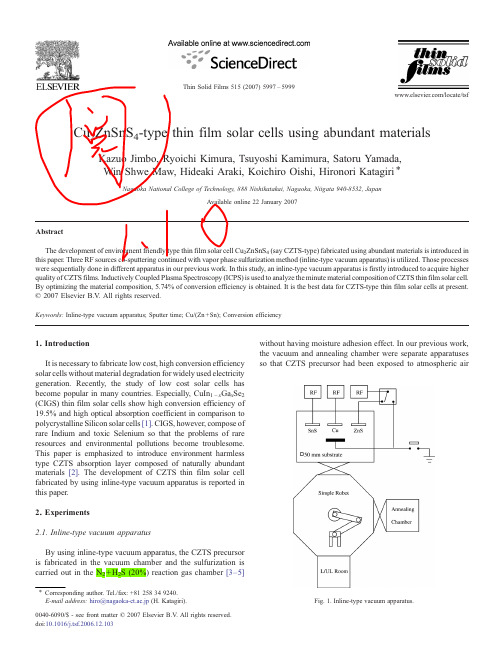
were sequentially done in different apparatus in our previous work.In this study,an inline-type vacuum apparatus is firstly introduced to acquire higher quality of CZTS films.Inductively Coupled Plasma Spectroscopy (ICPS)is used to analyze the minute material composition of CZTS thin film solar cell.By optimizing the material composition,5.74%of conversion efficiency is obtained.It is the best data for CZTS-type thin film solar cells at present.©2007Elsevier B.V .All rights reserved.Keywords:Inline-type vacuum apparatus;Sputter time;Cu/(Zn+Sn);Conversion efficiency1.IntroductionIt is necessary to fabricate low cost,high conversion efficiency solar cells without material degradation for widely used electricity generation.Recently,the study of low cost solar cells has become popular in many countries.Especially,CuIn 1−x Ga x Se 2(CIGS)thin film solar cells show high conversion efficiency of 19.5%and high optical absorption coefficient in comparison to polycrystalline Silicon solar cells [1].CIGS,however,compose of rare Indium and toxic Selenium so that the problems of rare resources and environmental pollutions become troublesome.This paper is emphasized to introduce environment harmless type CZTS absorption layer composed of naturally abundant materials [2].The development of CZTS thin film solar cell fabricated by using inline-type vacuum apparatus is reported in this paper.2.Experiments2.1.Inline-type vacuum apparatusBy using inline-type vacuum apparatus,the CZTS precursor is fabricated in the vacuum chamber and the sulfurization is carried out in the N 2+H 2S (20%)reaction gas chamber [3–5]without having moisture adhesion effect.In our previous work,the vacuum and annealing chamber were separate apparatuses so that CZTS precursor had been exposed to atmospheric air⁎Corresponding author.Tel./fax:+81258349240.E-mail address:hiro@nagaoka-ct.ac.jp (H.Katagiri).Fig.1.Inline-type vacuum apparatus.0040-6090/$-see front matter ©2007Elsevier B.V .All rights reserved.doi:10.1016/j.tsf.2006.12.103before it was annealed.The schematic diagram of the inline-type vacuum apparatus is shown in Fig.1.Three 10.16cm diameter cathodes with each RF sources are set up for three phased co-sputtering.CZTS thin film is fabricated by turning the substrate on the turned-table that can be heated up to 800°C before,after and/or during CZTS thin film fabricating process.The precursor can be automatically transferred to the SiC heater for annealing.Mass Flow Controllers are utilized to control the concentration of H 2S%.2.2.Experimental techniqueMo coated soda lime glass is used for fabrication of the precursor.The process started at the chamber pressure is in the order of 10−4Pa.The parameters of precursorfabrication are as follows;Ar gas flow rate:50sccm,Ar gas pressure:0.5Pa,substrate rotation:20rpm,pre-sputter time:3min,no substrate heating,applied target power:ZnS 160W,SnS 100W,Cu 95W for experiments A and variable Cu powers for experimets B.The finished precursor can be automatically transferred to the anneal chamber and then the chamber pressure is evacuated again to the vicinity of 10−4Pa.The reaction gas is injected to the chamber after closing the main valve.The annealing temperature was increased from room temperature to 580°C with a ramp rate of 5°C/min and is retained for 3h.Then the temperature was decreased to 200°C with the same ramp rate followed by natural cooling.The sample names are shown in Tables 1(a)and 1(b).The group of experiments A is done for the optimization of precursor thickness.The group B is carried out for the optimization of the Cu power within the range of 89W –98W.3.Results and discussions3.1.Experiments A (optimization of film thickness)The results of ICPS analysis are shown in Fig.2.As the sputter powers are set at constant for four samples,the ratios of Zn/Sn =1.18and Cu/(Zn +Sn)=0.94show nearly constantbehavior without a dependence on the thickness of CZTS film.S/Metal,however,decreases with increasing film thickness.This shows the excess sulfurization at thinner films.Moreover,it is obviously shown in the complete sulfurization throughout the CZTS film and is partially sulfurized on the upper surface of the lower electrode Mo by the observation of Scanning Electron Microscope.As the annealing temperature is constant,the thicknesses of sulfurized Mo show nearly the same indepen-dence on film thicknesses.The size of the crystal grains grows up with sputter time.The current versus voltage characteristics for the above four samples have shown that all samples have a maximum conversion efficiency of over 4%and the parallel resistances are smaller in the case of thinner films.The best sample A45has got a film thickness of 2.5μm,an open circuit voltage V oc =646mV,a short circuit current I sc =13.7mA/cm 2,a fill factor FF=0.60,a conversion efficiency =5.33%,a series resistance R s =6.41Ω,and a parallel resistance R p =424Ω.3.2.Experiments B (optimization of copper power)ICPS data are plotted as shown in Fig.3.Cu/(Zn +Sn)ratio is increasing with increasing Cu power although Zn/Sn =1.12and S/Metal =1.17remain nearly constant except in sample B98which shows that the process of sulfurization is insufficient.It is considerable to analyze the material compositions of the CZTS precursor together with the observation of the annealed CZTSTable 1(a)Sample names for experiments A Sputtering time (min)Sample name 15A1530A3045A4560A60Table 1(b)Sample names for experiments B Cu power (W)Sample Name 89B8992B9295B9598B98Fig.2.The result of the material composition analysis (experiments A).Fig.3.The result of the material composition analysis (experiments B).5998K.Jimbo et al./Thin Solid Films 515(2007)5997–5999film for a clear understanding of a complete sulfurized process. The surface morphology of the films was studied by SEM (see Fig.4).It shows an improvement of CZTS crystal grains with decreasing Cu power.Especially sample B89shows good appearance of1μm crystal grains with very few air voids.Fig.5 shows the current density versus voltage characteristic(I–V characteristic)of the sample B89.The samples B89–B95show a conversion efficiency of over4%.The sample B89shows an open circuit voltage V oc=662mV,a short circuit current I sc=15.7mA/cm2,a fill factor FF=0.55,a conversion efficiency=5.74%,a series resistance R s=9.04Ω,and a parallel resistance R p=612Ω.The material composition of the sample B89is Cu/(Zn+Sn)=0.87and Zn/Sn=1.15so called Cu-lean and Zn-rich type.It is also confirmed that50%of the electrodes of the cell has reached conversion efficiency of over4.5%.In our previous study,using separate vacuum chamber and anneal method,there was a remarkable dispersion of conversion efficiency even in a sample.In this study,however,the inline-type vacuum apparatus shows an improvement of consistency in conversion efficiency.This may be the effect of consecutive annealing without moisture adhesion onto the precursor surface. The quantum efficiency of65%is obtained at a wavelength of 480nm.The band gap energy of1.45eV is obtained by normalizing the quantum efficiency.The fill factor is decreasing with increasing Cu power(see Fig.6).The higher the Cu power, the lower the fill factor FF.It is known that the fill factor depends on the series and parallel resistances of solar cells.The material degradation of CZTS film in the case of higher Cu power shows the remarkable surface morphology in SEM observation.The nature of surface morphology in higher Cu power case shows the result of higher series resistance.This is one of the reasons of the decreasing fill factor.4.ConclusionsThis study reports the development of CZTS thin film solar cell by using inline-type vacuum apparatus.From the experi-ments A,the sample A45has got the thickness of2.5μm and 5.33%of conversion efficiency.From the experiments B,the sample B89with5.74%of conversion efficiency,Cu/(Zn+Sn) ratio of0.87,65%of the quantum efficiency at480nm is obtained.The band gap energy of1.45eV is obtained for both experiments.The fill factor FF is inversely proportional to the material composition ratio Cu/(Zn+Sn).By the fill factor versus Cu/(Zn+Sn)graph,it should be carefully observed whether the Cu power at the side of leaner ones can be obtained by the higher fill factor or not.According to the nature of dispersive electrical characteristics,the effect of electrodes may become important to get better consistent values.At present,the sample B89shows the best characteristics in the field of CZTS-type thin film solar cells.AcknowledgementsThis research is one of the consignments of New Energy and Industrial Technology Development Organization(NEDO)under the Ministry of Economy,Trade and Industry,Japan.The research place was offered from Nagaoka Business Incubation Center (NBIC)and Nagaoka University of Technology since it was struck by Niigata Prefecture Chuetsu earthquake.We would like to express our great reverence and special gratitude for all of you who concerned with this research,CZTS project.References[1]M.A.Contreras,et al.,Prog.Photovoltaics13(2005)209.[2]K.Ito,T.Nakazawa,Jpn.J.Appl.Phys27(1988)2094.[3]H.Katagiri,et al.,Sol.Energy Mater.Sol.Cells65(2001)141.[4]H.Katagiri,et al.,Jpn.J.Appl.Phys40(2001)500.[5]H.Katagiri,Thin Solid Films480–481(2005)426.Fig.4.The surface morphology by SEM(experiments B).Fig.5.The I–V characteristic of the sample B89.Fig.6.The characteristic of fill factor FF(experiments B).5999K.Jimbo et al./Thin Solid Films515(2007)5997–5999。
12、amorphous+silicon–based+solar+cells

Amorphous Silicon–based Solar Cells
Xunming Deng1 and Eric A. Schiff2
1
University of Toledo, Toledo, OH, USA, 2 Syracuse University, Syracuse, NY, USA
1 The
term amorphous is commonly applied to noncrystalline materials prepared by deposition from gases.
OVERVIEW
507
After several years of uncertainty, it emerged that plasma-deposited amorphous silicon contained a significant percentage of hydrogen atoms bonded into the amorphous silicon structure and that these hydrogen atoms were essential to the improvement of the electronic properties of the plasma-deposited material [9]. As a consequence, the improved form of amorphous silicon has generally been known as hydrogenated amorphous silicon (or, more briefly, a-Si:H). In recent years, many authors have used the term amorphous silicon to refer to the hydrogenated form, which acknowledges that the unhydrogenated forms of amorphous silicon are only infrequently studied today. Why was there so much excitement about the amorphous silicon solar cells fabricated by Carlson and Wronski? First, the technology involved is relatively simple and inexpensive compared to the technologies for growing crystals. Additionally, the optical properties of amorphous silicon are very promising for collecting solar energy, as we now explain. In Figure 12.2, the upper panel shows the spectrum for the optical absorption coefficients α(hν) for amorphous silicon and for crystalline silicon [10].2 In the lower panel of the figure, we show the spectrum of the “integrated solar irradiance;” this is the intensity (in W/m2 ) of the solar energy carried by photons above an energy threshold hν [11].
小学下册第十三次英语第1单元测验卷(有答案)

小学下册英语第1单元测验卷(有答案)考试时间:80分钟(总分:100)A卷一、综合题(共计100题共100分)1. 填空题:We can _____ (observe) plants in their natural habitat.2. 选择题:What is the capital of Vietnam?A. Ho Chi Minh CityB. HanoiC. Da NangD. Hue3. 选择题:What is the name of the famous theme park in California?A. Universal StudiosB. DisneylandC. SeaWorldD. Busch Gardens答案:B4. Depression started in the United States in ______ (1929年). 填空题:The Grea5. 选择题:What do we call the imaginary line that divides the Earth into northern and southern hemispheres?A. LatitudeB. EquatorC. MeridianD. Prime Meridian答案: B6. 听力题:Chemical reactions can release or absorb ________.What is the name of the toy that can fly?A. CarB. KiteC. TrainD. Boat8. 听力题:The ______ loves to play music.9. 选择题:What is the capital city of Italy?A. VeniceB. RomeC. MilanD. Florence答案:B10. 填空题:A ________ (墓地) can be found in historical sites.11. 选择题:What is the name of the famous giant in the children's story?A. JackB. BeanstalkC. GiantD. Cloud答案:C12. 填空题:Certain herbs are known for their ______ qualities, like lavender. (某些草药因其芳香特性而闻名,如薰衣草。
Professional+English+Solar+Cells

High performance materials
The materials used in professional English single cells are of high quality and have excellent optical and electrical properties These materials help to ensure that the solar cells absorb more sunlight and convert it into electricity more effectively
• Polycystalline solar cells: Made from multiple crystals of silicon, these cells are less effective but also less expensive
• Thin film solar cells: Made from thin layers of materials such as cadmium telluride or copper indium gallium selenium, these cells are the least effective but also the least expensive
03
Solar cells can significantly reduce greenhouse gas emissions and help to lower utility bills, making it an attractive option for homeowners
Commercial electricity
Advanced cell structures
有机太阳能电池 空穴转移主导激子解离
有机太阳能电池空穴转移主导激子解离下载温馨提示:该文档是我店铺精心编制而成,希望大家下载以后,能够帮助大家解决实际的问题。
文档下载后可定制随意修改,请根据实际需要进行相应的调整和使用,谢谢!并且,本店铺为大家提供各种各样类型的实用资料,如教育随笔、日记赏析、句子摘抄、古诗大全、经典美文、话题作文、工作总结、词语解析、文案摘录、其他资料等等,如想了解不同资料格式和写法,敬请关注!Download tips: This document is carefully compiled by theeditor.I hope that after you download them,they can help yousolve practical problems. The document can be customized andmodified after downloading,please adjust and use it according toactual needs, thank you!In addition, our shop provides you with various types ofpractical materials,such as educational essays, diaryappreciation,sentence excerpts,ancient poems,classic articles,topic composition,work summary,word parsing,copy excerpts,other materials and so on,want to know different data formats andwriting methods,please pay attention!有机太阳能电池:空穴转移在激子解离中的主导作用在当前的可再生能源领域,有机太阳能电池(Organic Solar Cells, OSCs)因其轻便、柔性以及低成本的特性,成为研究的热点。
用于环境催化的MoS2ZIF-8 复合材料——太阳能驱动的抗生素降解过程
ResearchEnvironmental Protection—ArticleMoS 2/ZIF-8Hybrid Materials for Environmental Catalysis:Solar-Driven Antibiotic-DegradationEngineeringWen-Qian Chen a ,c ,#,Lin-Yue Li a ,b ,#,Lin Li a ,Wen-Hui Qiu d ,e ,Liang Tang a ,b ,⇑,Ling Xu a ,Ke-Jun Xu a ,Ming-Hong Wu a ,b ,⇑aSchool of Environmental and Chemical Engineering,Shanghai University,Shanghai 200444,Chinab Key Laboratory of Organic Compound Pollution Control Engineering,Ministry of Education,Shanghai 200444,China cShanghai Institute of Applied Radiation,Shanghai University,Shanghai 201800,China dGuangdong Provincial Key Laboratory of Soil and Groundwater Pollution Control,School of Environmental Science and Engineering,Southern University of Science and Technology,Shenzhen 518055,China eState Environmental Protection Key Laboratory of Integrated Surface Water-Groundwater Pollution Control,School of Environmental Science and Engineering,Southern University of Science and Technology,Shenzhen 518055,Chinaa r t i c l e i n f o Article history:Received 11October 2018Revised 4February 2019Accepted 15February 2019Available online 4April 2019Keywords:1T/2H-MoS 2ZIF-8Antibiotic degradation Photocatalysisa b s t r a c tPhotocatalytic water purification is an efficient environmental protection method that can be used to eliminate toxic and harmful substances from industrial effluents.However,the TiO 2-based catalysts cur-rently in use absorb only a small portion of the solar spectrum in the ultraviolet (UV)region,resulting in lower efficiency.In this paper,we demonstrate a molybdenum disulfide/zeolitic imidazolate framework-8(MoS 2/ZIF-8)composite photocatalyst that increases the photocatalytic degradation of ciprofloxacin (CIP)and tetracycline hydrochloride (TC)by factors of 1.21and 1.07,respectively.The transformation products of CIP and TC from the catalysis processes are tentatively identified,with the metal–organic framework (MOF)being considered to be the main active species with holes being considered as the main active species.The hydrogen production rate of the MoS 2/ZIF-8nanocomposites is 1.79times higher than that of MoS 2.This work provides a novel perspective for exploring original and efficient 1T/2H-MoS 2/MOF-based photocatalysts by optimizing the construction of surface nano-heterojunction structures.The composite photocatalyst is found to be durable,with its catalytic performance being preserved under stability testing.Thus,1T/2H-MoS 2/MOF-based photocatalysts have excellent prospects for practical antibiotic-degradation engineering.Ó2019THE AUTHORS.Published by Elsevier LTD on behalf of Chinese Academy of Engineering and Higher Education Press Limited Company.This is an open access article under the CC BY-NC-ND license(/licenses/by-nc-nd/4.0/).1.IntroductionGiven the current global awareness of and attention to environ-mental pollution,the demand for new environmental-restoration technologies is increasing in many areas,including water pollution.One serious water pollution concern involves the abuse of a large number of broad-spectrum antibiotics,including ciprofloxacin (CIP)and tetracycline hydrochloride (TC),which end up in the water supply.Antibiotics pollution in water is known to be a major issue for human health [1–3].Over the past few years,various technologies to reduce antibiotics emission have been employed in environmental protection;these include physical adsorption [4,5],microbial degradation [6],and photocatalytic degradation [7].Among these,semiconductor-based photocatalysis is consid-ered to be an effective solution for antibiotics pollution in water due to its environmental friendliness,low energy consumption,and low cost [8,9].However,in comparison with pollutants such as dyes,it is relatively difficult to photodegrade antibiotics [10,11].Therefore,there is a great need for the development of new effective photocatalysts with higher antibiotic-degradation efficiency.Molybdenum disulfide (MoS 2)is a transition metal dichalco-genide catalyst with a structure that is similar to a two-dimensional (2D)graphene analog layered structure that has been attracting a great deal of attention in the catalysis of antibiotic degradation [12,13].The S A Mo A S coordination in the lattice is similar to a ‘‘sandwich”structure,and produces an unsaturatedhttps:///10.1016/j.eng.2019.02.0032095-8099/Ó2019THE AUTHORS.Published by Elsevier LTD on behalf of Chinese Academy of Engineering and Higher Education Press Limited Company.This is an open access article under the CC BY-NC-ND license (/licenses/by-nc-nd/4.0/).⇑Corresponding authors.E-mail addresses:tang1liang@ (L.Tang),mhwu@ (M.-H.Wu).#These authors contributed equally to this work.Engineering 5(2019)755–767Contents lists available at ScienceDirectEngineeringjo ur na l h o me pa ge :w w w.e ls ev ie r.c o m/lo c a t e/engphenomenon at the edges[14].In addition,MoS2has a tunable band gap structure,which varies from an indirect band gap of 1.2eV(for bulk MoS2)to an indirect band gap of1.8eV(for mono-layer MoS2)[15,16].However,the limitations of its narrow band gap and specific surface area impede the catalytic activity of MoS2.Therefore,MoS2has been constructed into different mor-phologies in order to improve its catalytic performances,including nanosheets,nanoparticles,and quantum dots.MoS2has two com-mon phases[17]:the metallic1T-MoS2,with more catalytically active sites,and the semiconducting2H-MoS2,with more active edge zones.It is necessary to synthesize mixed-phase MoS2with many active edge sites in order to maximize the photocatalytic activity of this catalyst.A metal–organic framework(MOF)is a kind of crystalline mate-rial with high porosity and a huge surface area,which has shown varying degrees of potential in catalysis application[18,19].Zeoli-tic imidazolate framework-8(ZIF-8)is a typical member of the MOF family that consists of zinc(Zn)ions and imidazole linkers. ZIF-8has been widely studied due to its high specific surface area, excellent thermal/chemical stability,and carbon dioxide(CO2) affinity[20,21].Thus,it is assumed that the combination of ZIF-8 nanocrystals with MoS2nanosheets will greatly increase the speci-fic surface area,adsorption,and number of photocatalytic reaction sites,thereby improving the photocatalytic degradation efficiency of the entire photocatalyst.In this work,we demonstrate that ZIF-8being tightly anchored on the1T/2H-MoS2nanosheets.In terms of catalytic performance,the composite catalyst shows greater photocatalytic antibiotic degradation activity than MoS2 on its own.2.Experiments2.1.Preparation of ZIF-8nanocrystalsThe ZIF-8was synthesized according to previously published procedures[22].In general, 1.81g of zinc nitrate hexahydrate (Zn(NO3)2Á6H2O)was dissolved in10mL of deionized(DI)water;1.0g of2-methylimidazole(2-MeIm,AR)was then dissolved in 10mL of ammonia solution(NH3ÁH2O,AR).Next,the2-MeIm solu-tion was slowly added in a drop-wise manner to the zinc nitrate solution,which was magnetically stirred at room temperature for 8h.Thefinal product was subsequently centrifuged and washed to neutrality.Finally,the white ZIF-8nanocrystal was obtained after freeze-drying for12h.2.2.Preparation of1T/2H-MoS2/ZIF-8composite1T/2H-MoS2/ZIF-8was prepared by a solvothermal method.In brief,0.151g(2mmol)thioacetamide(TAA,AR!99.0%),0.242g (1mmol)sodium molybdate(Na2MoO4,AR!99.0%),and0.05g (0.14mmol)cetyltrimethyl ammonium bromide(CTAB,AR)were dissolved in10mL DI water,which was stirred for5min to obtaina homogeneous solution.An amount of ZIF-8(a mass of8.0,11.2,16.0,24.0,or32.0mg)was then added to the mixed solution.Sub-sequently,40mL of N,N-dimethylformamide(DMF,AR!99.5%) was added to the mixed solution.After sonicating for2h,the mixed solution was transferred into a Teflon autoclave and kept in an oven at200°C for24h.Thefinal black product was cen-trifuged at8000rÁminÀ1and washed with75vol%ethanol.Finally, the prepared black product was freeze-dried for24h.The samples were marked as MZ-5,MZ-7,MZ-10,MZ-15,and MZ-20,where MZ refers to the MoS2/ZIF-8composite and the numbers refer to the weight content of ZIF-8(i.e.,5%,7%,10%,15%,and20%,respec-tively).The schematic synthesis procedure is shown in Fig.1.Pure MoS2was synthesized by a similar solvothermal method without the addition of ZIF-8.2.3.Characterization of1T/2H-MoS2/ZIF-8The phase structure of these samples was determined using D8 ADVANCED powder X-ray diffraction(XRD,Bruker Corporation, Germany).The microstructures and components of the as-prepared products were determined using a JEM-2010F transmis-sion electron microscope(TEM,JEOL Ltd.,Japan)and a FESEM-4800scanning electronic microscope(SEM,Hitachi Ltd.,Japan). The ultraviolet–visible light diffuse reflectance spectra(UV–vis DRS)were obtained using an Cary300spectrometer(Agilent Tech-nologies,USA).The excitation wavelength of the photolumines-cence(PL)spectrum was365nm(F-7000fluorescence spectrophotometer,Hitachi Ltd.,Japan).2.4.Photocatalytic activity measurementsThe photocatalytic degradation of aqueous solutions of CIP (purity!98.0%,20mgÁLÀ1)and TC(purity!98.0%,20mgÁLÀ1) was performed on1T/2H-MoS2/ZIF-8composites under visible light irradiation.A300W xenon(Xe)lamp(Nanjing Sidongke Elec-trical Equipment Co.,China)with a420nm cut-offfilter was used as a natural light source.In each test,a20mg sample of catalyst and50mL of the target pollutant(dissolved in water)were mixed in a quartz tube.Before irradiation,the solution was stirred for 30min under dark conditions.During irradiation,2mL of the mixed solution was taken out of the reactor andfiltered with a 0.45l m needlefilter.The absorbance peaks for CIP(276nm)and TC(357nm)were measured using a TU-1810spectrophotometer (PERSEE Ltd.,China)[23,24].The photocatalytic hydrogen(H2)evo-lution reactions were performed in an airtight quartz reactor with cooling water in order to maintain the reaction temperature at 25°C;a500W Xe lamp was used as a natural light source.Prior to irradiation,25mg of photocatalyst powder was dispersed in 50mL of15vol%triethanolamine(TEOA,AR)aqueous solution. During irradiation,H2was detected by a gas chromatograph (GC7920,Beijing CEAULIGHT Co.Ltd.,China)with nitrogen(N2) as the carrier gas.The area of the integrated peak of the gas chro-matography(GC)curve was compared with the area of the integral peak of the standard H2curve at a certain volume;the actual amount of H2was then calculated.The degradation intermediates were detected by means of high-performance liquid chromatogra-phy–tandem mass spectrometry(LC–MS/MS,6460Triple Quad LC–MS/MS,Agilent).Detailed analysis methods for the degradation products are provided in Appendix A.2.5.Photoelectrochemical performanceTransient photocurrent electrochemical impedance spec-troscopy(EIS)and Mott–Schottky plots were conducted on an elec-trochemical analyzer(CHI660E electrochemical workstation, Chenhua Instrument,Shanghai,China).The as-synthesized sam-ples were used as the working electrode,while a saturated calomel electrode(SCE)and a platinum sheet were used as the reference electrode and counter electrode,respectively.Detailed methods for the preparation of photoelectrodes are reported in the litera-ture[25].A500W Xe arc lamp with a420nm cut-offfilter was used as a light source.The Mott–Schottky tests were implemented using the impedance-potential mode.EIS tests were performed at an open-circuit potential in a frequency range between105and 10À2Hz in a dark environment.In all experiments,0.5molÁLÀ1 Na2SO4aqueous solution was used as the electrolyte.756W.-Q.Chen et al./Engineering5(2019)755–7673.Results and discussion3.1.Microstructures and componentsThe crystallinity of MoS 2and of the 1T/2H-MoS 2/ZIF-8nanocomposites was investigated by XRD;measurement results are displayed in Fig.2.The XRD pattern of the synthesized MoS 2was different from that of pristine 2H-MoS 2,as new (002)and sec-ond (002)*diffraction peaks of the as-synthesized MoS 2showed at 9.6°and 18.0°,respectively [26].According to the Bragg equation,the lattice spacing of the (002)plane was calculated to be 0.95nm (Fig.3(e)),which aligned with the interlayer distance from the TEM images.The increase in the interlayer distance of the MoS 2indirectly indicated that the prepared MoS 2was a metallic 1T phase [27].Fig.3(f)shows that a fringe spacing of 0.27nm can indicate the (100)crystal plane index of 2H-MoS 2.As indicated by Fig.S1(a),it is evident that in comparison with the standard value (JCPDS Card No.37-1492),the two diffraction peaks at 32.7°and 58.4°respectively indicate the (100)and (110)planes.The results indicate that the local atomic arrangement remains the same as that of the standard 2H-MoS 2structure [28],which confirms that the prepared MoS 2is a polytype phase.In addition,it can be seen from Fig.S1(b)that the MZ-20nanocomposite con-tains ZIF-8crystal,which signifies that the ZIF-8is in close contact with the MoS 2nanosheets.Fourier transform infrared (FT-IR)spec-troscopy of the MZ-7and ZIF-8are shown in Fig.4.The presence of ZIF-8is revealed by the following characteristic peaks:the band at 421cm À1is attributed to the Zn A N stretch,and other bands in the spectral region of 500–1500cm À1are due to plane bending and stretching of the imidazole ring [29].It is worth noting that the same adsorption bands were observed for the MZ-7nanomaterial.For MZ nanomaterials,it can be seen that the characteristic peaks are consistent with those of pure MoS 2(Fig.S2),which confirms that the metal-phase MoS 2was successfully prepared.We examined pure MoS 2,MZ-7,and MZ-20samples by SEM (Fig.S3)and TEM (Fig.3)to understand the degree of complexation of the ZIF-8crystals with MoS 2.As shown in Figs.S3(a,b),MZ-7exhibits a flower-like structure.Furthermore,these lamella flowers are not completely isolated from each other,but are often superim-posed together.Small particles of ZIF-8fit tightly on the flower-like 1T/2H-MoS 2surface.Careful observation of the morphology of MZ-7shows that many curled and staggered nanosheets grow densely on the surface.In MZ-20,the flower-like structure gradually disap-pears,showing a smooth surface covered by ZIF-8.The probable reason for this structural change is that the increasing content of ZIF-8affects the anisotropic growth and flower-like structureformation of the 1T/2H-MoS 2.As indicated in Figs.3(a–d),which shows TEM images of a single MZ-7petal nanosheet,the 1T/2H-MoS 2nanosheets are curled to form tubular structures.ZIF-8par-ticles are partially attached to the tubular 1T/2H-MoS 2structures.Under electron beam irradiation,these nanosheets are extremely transparent,which indicates that the sheets are very thin (Figs.3(b,c)).An ultrathin tubular structure is more conducive to the rapid transmission of photo-induced electrons,and thus reduces the recombination rate.Fig.5shows the presence of the elements sulfur (S),molybdenum (Mo),Zn,nitrogen (N),and carbon (C)in the MZ-7nanocomposite.It is notable that these elements are uniformly distributed throughout the MZ-7,and it is further confirmed that the ZIF-8is very uniformly dispersed and attached to the 1T/2H-MoS 2.The pore characteristics of the as-prepared samples were investigated by the N 2physical sorption method (Fig.6).The N 2adsorption/desorption isotherms of MZ-5,MZ-7,MZ-10,MZ-15,and MZ-20are type IV adsorption curves (Figs.6and S4(a–c)).At higher relative pressures (P =P 0),the MZ-7sample exhibits higher adsorption performance compared with other prepared samples,which reveals the existence of cumulative pores [30].Unlike the MZ nanocomposites,a distinctive type I isotherm is shown by the ZIF-8(Fig.S4(d)).The specific surface areas of MZ-5,MZ-7,MZ-10,MZ-15,and MZ-20were measured to be 17.789,33.308,25.150,11.482,and 27.354m 2Ág À1,respectively (Table S1).These findings show that MZ-7provides more adsorptionandFig.1.A schematic illustration of the preparation of MZnanocomposites.Fig.2.XRD patterns of MoS 2and MZ.W.-Q.Chen et al./Engineering 5(2019)755–767757photocatalytic active sites than the other nanocomposites.In addition,as shown in the inset of Fig.6(a),MZ-7mainly contains mesoporous types (2–8nm)corresponding to the Barrett–Joyner–Halenda pore-size distribution curve.Furthermore,the pore-size distribution curve of MZ-20shows that the main pore-size range is 1–6nm (inset Fig.6(b)).This may be because the addition of ZIF-8affects the particle size of 1T/2H-MoS 2.The synergistic effect of its various pores and the high specific surface area of MZ-7are conducive to the rapid mass transfer of the target contaminant molecules and diffusion of photo-induced electrons [31];thus,MZ-7is expected to display excellent photocatalytic degradation.The elemental composition and functional characterization of the 1T/2H-MoS 2/ZIF-8nanomaterials were further confirmed by X-ray photoelectron spectroscopy (XPS).In Fig.7(a),the XPS survey spectrum shows that MZ-7mainly consists of the elements S,Mo,Zn,C,and N.The XPS results of S 2p are displayed in Fig.7(b).The MZ-7has three peaks at 163.8,162.4,and 160.9eV that can be assigned to S 2p 1/2and S 2p 3/2[32].As shown in Fig.7(c),the Mo 3d binding energy spectrum of MZ-7has four peaks at 235.0,231.7,228.1,and 225.3eV,which corroborate the presence of Mo 3d 5/2and 3d 3/2[23].When the S 2p and Mo 3d spectra of MZ-7and MoS 2are compared,the result indicates that the S 2p and Mo 3d spectra of MZ-7shift to higher binding energies by 0.7eV,which satisfies the previously observed relaxation energy before the formation of 1T-MoS 2.A significant increase in bindingenergyFig.3.(a–d)TEM images and (e,f)high-magnification TEM images of the MZ-7nanocomposites.Fig.4.FT-IR spectra of MZ-7and ZIF-8.758W.-Q.Chen et al./Engineering 5(2019)755–767of 0.70eV usually indicates a loss of electron density [33],which can generate more active vacancies and thus increase the photo-catalytic effect.As illustrated in Figs.7(d–f),the results suggest that the composite MZ-7,which includes ZIF-8,contains the elements Zn,C,and N.Two peaks are observed at 1044.0eV (Zn 2p1/2)and 1020.9eV (Zn 2p3/2),respectively,which correspond to the Zn 2+of the ZIF-8(Fig.7(d)).As a comparison,the Zn 2p peaks of ZIF-8are located at 1044.7eV and 1021.6eV.MZ-7shows a neg-ative shift of 0.7eV relative to ZIF-8,which may be due to electron transfer [34].In the C 1s XPS spectrum (Fig.7(e)),three binding energies of MZ-7peak at 288.5,285.9,and 284.5eV;these can be assigned to the carboxyl carbon (O @C A O),hydroxyl carbon (C A O),and sp 2-hybridized carbon (C A C)[35].In Fig.7(f),the N 1s band peaks are 398.8,397.0,and 394.5eV;these can be attrib-uted to the C A N bond and the 2-methylimidazole nitrogen atoms [36].The XPS results reveal that MoS 2fits snugly on the ZIF-8sur-face,and that specific elements are prominently present in the composite.It is evident that the positions of the S 2p,Mo 3d,and Zn 2p peaks in MoS 2/ZIF-8are shifted a little,indicating that the MoS 2and ZIF-8are interacting with each other.It is likely that the ZIF-8nanocrystals become embedded in the MoS 2nanosheets during the solvent heat treatment [37].Thus,the above analyses indicate that 1T/2H-MoS 2was successfully synthesized in this work.More importantly,the results suggest that the prepared samples have more active sites and more significant photocatalytic effects than MoS 2or ZIF-8on their own.The absorbance performance of the MZ nanocomposites and MoS 2was measured using UV–vis DRS.Fig.8(a)shows that all samples display significantly enhanced light absorption between 200and 800nm.The characteristic absorption for pure ZIF-8isFig.5.Energy-dispersive spectroscopy (EDS)elemental mappings of the obtained MZ-7nanocomposites.Fig.6.N 2sorption isotherms and pore-size distribution of the (a)MZ-7and (b)MZ-20composites.STP:standard temperature and pressure.W.-Q.Chen et al./Engineering 5(2019)755–767759detected at around 225nm (Fig.S5(a)).However,when ZIF-8is loaded with 1T/2H-MoS 2,the light absorption capacity is significantly improved,indicating the importance of the hybrid composite in enhancing photocatalysis.This finding means that the higher visible light absorption of the heterojunction between ZIF-8and 1T/2H-MoS 2leads to the photogeneration of electron-hole pairs,which further promote the photocatalytic performance.The relationship between the wavelength of different nanocom-posites and the photon energy (eV)can be calculated by the Kubelka–Munk function (K–M function),provided below [38]:F R ðÞ¼1ÀR ðÞ22Rð1Þwhere R is the reflectance and F R ðÞis proportional to the absorption coefficient (a ).The relationship between the K–M function and the wavelength of all the synthesized composites is shown in Fig.8(b).As shown inFigs.8(c,d),the band gap energies (E g )of 1T/2H-MoS 2and ZIF-8areestimated from the tangent to the curve of a h m ðÞ1=2(or a h m ðÞ2)with respect to the photo-energy.The band gaps of 1T/2H-MoS 2,ZIF-8,and MZ-7(Fig.S5(b))are 1.13,5.12,and 1.05eV,respectively,indi-cating that the introduction of 1T/2H-MoS 2reduced the band gaps.All the results suggest that the visible light response of the sample is increased;it can now generate more photogenerated carriers to improve the photocatalytic performance.3.2.Photocatalytic propertiesTo assess the potential use of the MZ samples in environmental remediation,their photocatalytic activities were evaluated in terms of the photocatalytic degradation of CIP and TC.As can be observed from Fig.9(a),all samples exhibit catalytic properties in the degradation of CIP.Among the samples,MZ-7has the highest catalytic efficiency,which is in agreement with theBrunauer–Fig.7.XPS spectra of MZ-7compared with pure MoS 2and ZIF-8.(a)Survey scan;(b)S 2p;(c)Mo 3d;(d)Zn 2p;(e)C 1s;(f)N 1s.760W.-Q.Chen et al./Engineering 5(2019)755–767Emmett–Teller (BET)surface area analysis.As the content of ZIF-8increases,the catalytic performance of the samples improves at first,and then gradually decreases.After irradiation for 180min under visible light,the photodegradation rates of CIP by the MZ-7hybrids increased to 93.2%,which is 1.21times greater than that of pure MoS 2.Fig.9(b)depicts the photodegradation kinetics for CIP by the MZ nanocomposites with different amounts of ZIF-8,and by pure MoS 2.The kinetic curve of CIP degradation is in accor-dance with the pseudo first-order linear transformation ln C =C 0ðÞ¼Àkt [39].Meanwhile,the pseudo first-order reaction kinetics (k )value of MZ-7(0.0099min À1)is 1.29times and 1.71times higher than those of MZ-20and pure MoS 2,respectively;this can be attributed to the coupling of the nanostructured sheets and ZIF-8within the ultrathin structure of 1T/2H-MoS 2,which provides a pathway for the rapid transfer of photogenerated charge carriers.The small amount of CTAB helps 1T/2H-MoS 2to generate ultrathin nanosheets [40].It is worth noting that the removal efficiency of TC reaches 75.6%in the presence of the photocatalyst MZ-7at 180min under visible light irradiation (Fig.9(c)).As seen in Fig.9(d),k for the removal of TC on MZ-7is 0.0049min À1(1.53times greater than that of MZ-15).This can be ascribed to the rapid separation role of the photogenerated charge carriers by the 1T-MoS 2.Another important factor is that the porous ZIF-8provides more reactive sites and enhances the progress of photocatalytic degradation.Interestingly,the photocatalytic activity can be improved by dop-ing ZIF-8on the surface of 1T/2H-MoS 2.1T-MoS 2has excellent electrical conductivity and accelerates the transmission of photo-excited electrons,while 2H-MoS 2provides many active attach-ment sites on the edge.In addition,ZIF-8increases the specific sur-face area of MZ-7,giving it more catalytic centers.Moreover,the synergistic effect between 1T/2H-MoS 2and ZIF-8plays an impor-tant role in the degradation of CIP and TC.The photocatalytic activities were assessed by photocatalytic hydrogen evolution reaction in TEOA aqueous solution under visible light irradiation (k !420nm).As shown in Fig.S6,the content of ZIF-8significantly affected the efficiency of hydro-gen production.This test indicated that MZ-7has the greatest photocatalytic activity,with a hydrogen production rate of 61.45l mol Áh À1Ág À1,which is 1.79times greater than that of pure MoS 2.Thus,the test indicated that the addition of an appropriate amount of ZIF-8improved the catalytic activity of 1T/2H-MoS 2for hydrogen production,by increasing the con-ductivity of the material and providing a larger surface of the exposed edges.These findings also explain the improved pho-tocatalytic activity,which is due to the presence of mixed states and induced structural distortions at the boundaries of the MZ-7[41].A more rigorous analysis of these results revealed that a good interfacial heterojunction between 1T/2H-MoS 2and ZIF-8contributes to an efficient charge trans-fer and e ––h +separation.3.3.Repeatability and stability of the MZ compositesIn order to evaluate the application possibilities of this catalyst in the environment,the reusability and stability of MZ-7were also tested.The target pollutant of the cyclic test was replaced with CIP with a solution concentration of 20mg ÁL À1,and the mass of the photocatalyst was 20mg.As seen in Fig.10(a),after two cycles of CIP degradation,the removal rate of CIP was still 90%at the 3rd run within 180min.The photocatalytic activity of MZ-7did not decrease significantly,which indicates that the MZ-7photocatalyst has high stability and can be used repeatedly in practical applications.The XRD result showed that the MZ-7was chemically stable before and after the reaction (Fig.10(b)).Fig.8.(a)UV–vis DRS spectra of MZ nanocomposites and pure MoS 2;(b)plot of K–M function estimated from UV–vis DRS spectra of MZ nanocomposites;(c)plot of a h m ðÞ1=2vs.photo-energy (h m )of pure MoS 2;(d)plot of a h m ðÞ2vs.photo-energy (h m )of ZIF-8.W.-Q.Chen et al./Engineering 5(2019)755–7677613.4.Discussion of the photocatalytic mechanismAlthough we obtained a captivating antibiotic-degradation per-formance with the MZ-7composite,in order to further clarify the photocatalysis mechanism,radical scavenging experiments were conducted.Three typical scavengers (dosage:1mmol ÁL À1)—iso-propyl alcohol,EDTA-2Na,and q -benzoquinone—were employed as the scavengers of _OH,h +,and _O À2,respectively [42].For these experiments,the aqueous solution of CIP was 20mg ÁL À1and the sample quantity was 20mg.As shown in Fig.11(a),the photocat-alytic degradation of CIP was significantly inhibited after the addi-tion of EDTA-2Na,implying that h +plays an active role inphotocatalytic reactions.Furthermore,the photodegradation of CIP was inhibited in the presence of isopropanol,confirming that _OH plays a minor role in photocatalysis.However,the degradation of CIP after the addition of p -benzoquinone was comparable to the absence of sacrificial agent.The PL spectra shown in Fig.11(b)provides information on the separation efficiency of the photo-induced electron–hole (e ––h +)pairs [43].It is shown that the combination of ZIF-8and 1T/2H-MoS 2can severely reduce PL intensity,which confirms that the recombination of e ––h +pairs transferred to the surface of the ZIF-8is hindered.This result is understandable because the flower-like 1T/2H-MoS 2is more conductive to the rapidtransferFig.9.Photodegradation efficiency and photodegradation rate constants for (a,b)CIP and (c,d)TC by MZ nanomaterials and pure MoS 2.C =C 0:normalizedconcentration.Fig.10.(a)Recycled performance chart for the MZ-7composite for CIP;(b)XRD images of the MZ-7composite before and after the photocatalytic reaction.762W.-Q.Chen et al./Engineering 5(2019)755–767。
光伏发电英文文献Ultra-High Efficiency Photovoltaic
Ultra-High Efficiency Photovoltaic Cells for Large Scale Solar Power GenerationYoshiaki NakanoAbstract The primary targets of our project are to dras-tically improve the photovoltaic conversion efficiency and to develop new energy storage and delivery technologies. Our approach to obtain an efficiency over40%starts from the improvement of III–V multi-junction solar cells by introducing a novel material for each cell realizing an ideal combination of bandgaps and lattice-matching.Further improvement incorporates quantum structures such as stacked quantum wells and quantum dots,which allow higher degree of freedom in the design of the bandgap and the lattice strain.Highly controlled arrangement of either quantum dots or quantum wells permits the coupling of the wavefunctions,and thus forms intermediate bands in the bandgap of a host material,which allows multiple photon absorption theoretically leading to a conversion efficiency exceeding50%.In addition to such improvements, microfabrication technology for the integrated high-effi-ciency cells and the development of novel material systems that realizes high efficiency and low cost at the same time are investigated.Keywords Multi-junctionÁQuantum wellÁConcentratorÁPhotovoltaicINTRODUCTIONLarge-scale photovoltaic(PV)power generation systems, that achieve an ultra-high efficiency of40%or higher under high concentration,are in the spotlight as a new technology to ease drastically the energy problems.Mul-tiple junction(or tandem)solar cells that use epitaxial crystals of III–V compound semiconductors take on the active role for photoelectric energy conversion in such PV power generation systems.Because these solar cells operate under a sunlight concentration of5009to10009, the cost of cells that use the epitaxial crystal does not pose much of a problem.In concentrator PV,the increased cost for a cell is compensated by less costly focusing optics. The photons shining down on earth from the sun have a wide range of energy distribution,from the visible region to the infrared region,as shown in Fig.1.Multi-junction solar cells,which are laminated with multilayers of p–n junctions configured by using materials with different band gaps,show promise in absorbing as much of these photons as possible,and converting the photon energy into elec-tricity with minimum loss to obtain high voltage.Among the various types of multi-junction solar cells,indium gallium phosphide(InGaP)/gallium arsenide(GaAs)/ger-manium(Ge)triple-junction cells that make full use of the relationship between band gaps and diverse lattice con-stants offered by compound semiconductors have the advantage of high conversion efficiency because of their high-quality single crystal with a uniform-size crystal lat-tice.So far,a conversion efficiency exceeding41%under conditions where sunlight is concentrated to an intensity of approximately5009has been reported.The tunnel junction with a function equivalent to elec-trodes is inserted between different materials.The positive holes accumulated in the p layer and the electrons in the adjacent n layer will be recombined and eliminated in the tunnel junction.Therefore,three p–n junctions consisting of InGaP,GaAs,and Ge will become connected in series. The upper limit of the electric current is set by the mini-mum value of photonflux absorbed by a single cell.On the other hand,the sum of voltages of three cells make up the voltage.As shown in Fig.1,photons that can be captured in the GaAs middle cell have a smallflux because of the band gap of each material.As a result,the electric currentoutputAMBIO2012,41(Supplement2):125–131 DOI10.1007/s13280-012-0267-4from the GaAs cell theoretically becomes smaller than that of the others and determines the electric current output of the entire tandem cell.To develop a higher efficiency tandem cell,it is necessary to use a material with a band gap narrower than that of GaAs for the middle cell.In order to obtain maximum conversion efficiency for triple-junction solar cells,it is essential to narrow down the middle cell band gap to 1.2eV and increase the short-circuit current density by 2mA/cm 2compared with that of the GaAs middle cell.When the material is replaced with a narrower band gap,the output voltage will drop.However,the effect of improving the electric current balance out-performs this drop in output voltage and boosts the effi-ciency of the entire multi-junction cell.When a crystal with such a narrow band gap is grown on a Ge base material,lattice relaxation will occur in the middle of epitaxial crystal growth because the lattice constants of narrower band-gap materials are larger than that of Ge (as shown in Fig.2).As a result,the carrier transport properties will degrade due to dislocation.Researchers from the international research center Solar Quest,the University of Tokyo,aim to move beyond such material-related restrictions,and obtain materials and structures that have effective narrow band gaps while maintaining lattice matching with Ge or GaAs.To achieve this goal,we have taken three approaches as indicated in Fig.3.These approaches are explained in detail below.DILUTE NITROGEN-ADDED BULK CRYSTAL Indium gallium nitride arsenide (InGaNAs)is a bulk material consists of InGaAs,which contains several percent of nitrogen.InGaNAs has a high potential for achieving a narrow band gap while maintaining lattice matching with Ge or GaAs.However,InGaNAs has a fatal problem,that is,a drop in carrier mobility due to inhomogeneousdistribution of nitrogen (N).To achieve homogeneous solid solution of N in crystal,we have applied atomic hydrogen irradiation in the film formation process and addition of a very small amount of antimony (Sb)(Fig.3).The atomic hydrogen irradiation technology and the nitrogen radical irradiation technology for incorporating N efficiently into the crystal can be achieved only through molecular beam epitaxy (MBE),which is used to fabricate films under high vacuum conditions.(Nitrogen radical irradiation is a technology that irradiates the surface of a growing crystal with nitrogen atoms that are resolved by passing nitrogen through a plasma device attached to the MBE system.)Therefore,high-quality InGaNAs has been obtained only by MBE until now.Furthermore,as a small amount of Sb is also incorporated in a crystal,it is nec-essary to control the composition of five elements in the crystal with a high degree of accuracy to achieve lattice matching with Ge or GaAs.We have overcome this difficulty by optimizing the crystal growth conditions with high precision and devel-oped a cell that has an InGaNAs absorption layer formed on a GaAs substrate.The short-circuit current has increased by 9.6mA/cm 2for this cell,compared with a GaAs single-junction cell,by narrowing the band gap down to 1.0eV.This technology can be implemented not only for triple-junction cells,but also for higher efficiency lattice-matched quadruple-junction cells on a Ge substrate.In order to avoid the difficulty of adjusting the compo-sition of five elements in a crystal,we are also taking an approach of using GaNAs with a lattice smaller than that of Ge or GaAs for the absorption layer and inserting InAs with a large lattice in dot form to compensate for the crystal’s tensile strain.To make a solid solution of N uniformly in GaNAs,we use the MBE method for crystal growth and the atomic hydrogen irradiation as in the case of InGaNAs.We also believe that using 3D-shaped InAs dots can effectively compensate for the tensile strainthatFig.1Solar spectrum radiated on earth and photon flux collected by the top cell (InGaP),middle cell (GaAs),and bottom cell (Ge)(equivalent to the area of the filled portions in the figure)occurs in GaNAs.We have measured the characteristics of a single-junction cell formed on a GaAs substrate by using a GaNAs absorption layer with InAs dots inserted.Figure 4shows that we were able to succeed in enhancing the external quantum efficiency in the long-wavelength region (corresponding to the GaNAs absorp-tion)to a level equal to GaAs.This was done by extending the absorption edge to a longer wavelength of 1200nm,and increasing the thickness of the GaNAs layer by increasing the number of laminated InAs quantum dot layers.This high quantum efficiency clearly indicates that GaNAs with InAs dots inserted has the satisfactory quality for middle cell material (Oshima et al.2010).STRAIN-COMPENSATED QUANTUM WELL STRUCTUREIt is extremely difficult to develop a narrow band-gap material that can maintain lattice matching with Ge orGaAs unless dilute nitrogen-based materials mentioned earlier are used.As shown in Fig.2,the conventionally used material InGaAs has a narrower band gap and a larger lattice constant than GaAs.Therefore,it is difficult to grow InGaAs with a thickness larger than the critical film thickness on GaAs without causing lattice relaxation.However,the total film thickness of InGaAs can be increased as an InGaAs/GaAsP strain-compensated multi-layer structure by laminating InGaAs with a thickness less than the critical film thickness in combination with GaAsP that is based on GaAs as well,but has a small lattice constant,and bringing the average strain close to zero (Fig.3.).This InGaAs/GaAsP strain-compensated multilayer structure will form a quantum well-type potential as shown in Fig.5.The narrow band-gap InGaAs layer absorbs the long-wavelength photons to generate electron–hole pairs.When these electron–hole pairs go over the potential bar-rier of the GaAsP layer due to thermal excitation,the electrons and holes are separated by a built-in electricfieldFig.2Relationship between band gaps and lattice constants of III–V-based and IV-based crystalsto generate photocurrent.There is a high probability of recombination of electron–hole pairs that remain in the well.To avoid this recombination,it is necessary to take out the electron–hole pairs efficiently from the well and transfer them to n-type and p-type regions without allowing them to be recaptured into the well.Designing thequantumFig.3Materials and structures of narrow band-gap middle cells being researched by thisteamFig.4Spectral quantum efficiency of GaAs single-junction cell using GaNAs bulk crystal layer (inserted with InAs dots)as the absorption layer:Since the InAs dot layer and the GaNAs bulk layer are stacked alternately,the total thickness of GaNAs layers increases as the number of stacked InAs dot layers is increased.The solid line in the graph indicates the data of a reference cell that uses GaAs for its absorption layer (Oshima et al.2010)well structure suited for this purpose is essential for improving conversion efficiency.The high-quality crystal growth by means of the metal-organic vapor phase epitaxy (MOVPE)method with excellent ability for mass production has already been applied for InGaAs and GaAsP layers in semiconductor optical device applications.Therefore,it is technologically quite possible to incorporate the InGaAs/GaAsP quantum well structure into multi-junction solar cells that are man-ufactured at present,only if highly accurate strain com-pensation can be achieved.As the most basic approach related to quantum well structure design,we are working on fabrication of super-lattice cells with the aim of achieving higher efficiency by making the GaAsP barrier layer as thin as possible,and enabling carriers to move among wells by means of the tunnel effect.Figure 6shows the spectral quantum effi-ciency of a superlattice cell.In this example,the thickness of the GaAsP barrier layer is 5nm,which is not thin enough for proper demonstration of the tunnel effect.When the quantum efficiency in the wavelength range (860–960nm)that corresponds to absorption of the quan-tum well is compared between a cell,which has a con-ventionally used barrier layer and a thickness of 10nm or more,and a superlattice cell,which has the same total layer thickness of InGaAs,the superlattice cell demonstrates double or higher quantum efficiency.This result indicates that carrier mobility across quantum wells is promoted by even the partial use of the tunnel effect.By increasing the P composition in the GaAsP layer,the thickness of well (or the In composition)can be increased,and the barrier layer thickness can be reduced while strain compensation is maintained.A cell with higher quantum efficiency can befabricated while extending the absorption edge to the long-wavelength side (Wang et al.2010,2012).GROWTH TECHNIQUE FOR STRAIN-COMPENSATED QUANTUM WELLTo reduce the strain accumulated in the InGaAs/GaAsP multilayer structure as close to zero as possible,it is nec-essary to control the thickness and atomic content of each layer with high accuracy.The In composition and thickness of the InGaAs layer has a direct effect on the absorption edge wavelength and the GaAsP layer must be thinned to a satisfactory extent to demonstrate fully the tunnel effect of the barrier layer.Therefore,it is desirable that the average strain of the entire structure is adjusted mainly by the P composition of the GaAsP layer.Meanwhile,for MOVPE,there exists a nonlinear rela-tionship between the P composition of the crystal layer and the P ratio [P/(P ?As)]in the vapor phase precursors,which arises from different absorption and desorption phenomena on the surface.As a result,it is not easy to control the P composition of the crystal layer.To break through such a difficulty and promote efficient optimiza-tion of crystal growth conditions,we have applied a mechanism to evaluate the strain of the crystal layer during growth in real time by sequentially measuring the curvature of wafers during growth with an incident laser beam from the observation window of the reactor.As shown in Fig.7,the wafer curvature during the growth of an InGaAs/GaAsP multilayer structure indicates a periodic behavior.Based on a simple mechanical model,it has become clear that the time changes ofwaferFig.5Distribution of potential formed by the InGaAs/GaAsP strain-compensated multilayer structure:the narrow band-gap InGaAs layer is sandwiched between wide band-gap GaAsP layers and,as a result,it as quantum well-type potential distribution.In the well,electron–hole pairs are formed by absorption of long-wavelength photons and at the same time,recombination of electrons and holes takes place.The team from Solar Quest is focusing on developing a superlattice structure with the thinnest GaAsP barrier layercurvature are proportionate to the strain of the crystal layer relative to a substrate during the growing process.One vibration cycle of the curvature is same as the growth time of an InGaAs and GaAsP pair (Sugiyama et al.2011).Therefore,the observed vibration of the wafer curvature reflects the accumulation of the compression strain that occurs during InGaAs growth and the release of the strain that occurs during GaAsP growth.When the strain is completely compensated,the growth of the InGaAs/GaAsP pair will cause this strain to return to the initial value and the wafer curvature will vibrate with the horizontal line as the center.As shown in Fig.7,strain can be compensated almost completely by adjusting the layer structure.Only by conducting a limited number of test runs,the use of such real-time observation technology of the growth layer enables setting the growth conditions for fabricating the layer structure for which strain has been compensated with highaccuracy.Fig.6Spectral quantum efficiency of GaAs single-junction cell using InGaAs/GaAsP superlattice as theabsorption layer:This structure consists of 60layers of InGaAs quantum wells.The graph also shows data of a reference cell that uses GaAs for its absorption layer (Wang et al.2010,2012)Fig.7Changes in wafer curvature over time during growth of the InGaAs/GaAsP multilayer structure.This graph indicates the measurement result and the simulation result of the curvature based on the layer structure(composition ?thickness)obtained by X-ray diffraction.Since compressive strain is applied during InGaAs growth,the curvature decreases as time passes.On the other hand,since tensile strain is applied during GaAsP growth,the curvature changes in the oppositedirection (Sugiyama et al.2011)FUTURE DIRECTIONSIn order to improve the conversion efficiency by enhancing the current matching of multi-junction solar cells using III–V compound semiconductors,there is an urgent need to create semiconductor materials or structures that can maintain lattice matching with Ge or GaAs,and have a band gap of1.2eV.As for InGaNAs,which consists of InGaAs with several percent of nitrogen added,we have the prospect of extending the band edge to1.0eV while retaining sufficient carrier mobility for solar cells by means of atomic hydrogen irradiation and application of a small quantity of Sb during the growth process.In addition,as for GaNAs bulk crystal containing InAs dots,we were able to extend the band edge to1.2eV and produce a high-quality crystal with enoughfilm thickness to achieve the quantum efficiency equivalent to that of GaAs.These crystals are grown by means of MBE. Therefore,measures that can be used to apply these crys-tals for mass production,such as migration to MOVPE, will be investigated after demonstrating their high effi-ciency by embedding these crystals into multi-junction cells.As for the InGaAs/GaAsP strain-compensated quantum well that can be grown using MOVPE,we are working on the development of a thinner barrier layer while compen-sating for the strain with high accuracy by real-time observation of the wafer curvature.We have had the prospect of achieving a quantum efficiency that will sur-pass existing quantum well solar cells by promoting the carrier transfer within the multilayer quantum well struc-ture using the tunnel effect.As this technology can be transferred quite easily to the existing multi-junction solar cell fabrication process,we strongly believe that this technology can significantly contribute to the efficiency improvement of the latest multi-junction solar cells. REFERENCESOshima,R.,A.Takata,Y.Shoji,K.Akahane,and Y.Okada.2010.InAs/GaNAs strain-compensated quantum dots stacked up to50 layers for use in high-efficiency solar cell.Physica E42: 2757–2760.Sugiyama,M.,K.Sugita,Y.Wang,and Y.Nakano.2011.In situ curvature monitoring for metalorganic vapor phase epitaxy of strain-balanced stacks of InGaAs/GaAsP multiple quantum wells.Journal of Crystal Growth315:1–4.Wang,Y.,Y.Wen,K.Watanabe,M.Sugiyama,and Y.Nakano.2010.InGaAs/GaAsP strain-compensated superlattice solar cell for enhanced spectral response.In Proceedings35th IEEE photovoltaic specialists conference,3383–3385.Wang,Y.P.,S.Ma,M.Sugiyama,and Y.Nakano.2012.Management of highly-strained heterointerface in InGaAs/GaAsP strain-balanced superlattice for photovoltaic application.Journal of Crystal Growth.doi:10.1016/j.jcrysgro.2011.12.049. AUTHOR BIOGRAPHYYoshiaki Nakano(&)is Professor and Director General of Research Center for Advanced Science and Technology,the University of Tokyo.His research interests include physics and fabrication tech-nologies of semiconductor distributed feedback lasers,semiconductor optical modulators/switches,monolithically integrated photonic cir-cuits,and high-efficiency heterostructure solar cells.Address:Research Center for Advanced Science and Technology, The University of Tokyo,4-6-1Komaba,Meguro-ku,Tokyo153-8904,Japan.e-mail:nakano@rcast.u-tokyo.ac.jp。
全国大学英语CET六级考试试题及解答参考

全国大学英语CET六级考试复习试题及解答参考一、写作(15分)Writing (30 minutes)Part AFor this part, you are allowed 30 minutes to write an essay on the following topic: “The Role of Technology in Education”. You should write at least 150 words but no more than 200 words. You should base your essay on the chart below and give reasonable explanations for your views.Chart: The Impact of Technology on EducationYear | Number of Students Using Technology-----------------------2000 | 10%2005 | 30%2010 | 60%2015 | 90%2020 | 95%Example Essay:The chart above clearly illustrates the significant increase in the number of students using technology in education over the past two decades. This trend is not surprising, given the rapid advancements in technology and its integration into various aspects of our lives.In my opinion, the role of technology in education is multifaceted. Firstly, it has revolutionized the way students learn. With access to the internet and educational platforms, students can now access a wealth of information and resources, which enhances their learning experience. This has made education more personalized and adaptable to individual learning styles.Secondly, technology has made education more inclusive. Online courses and distance learning programs have opened up educational opportunities for students who are unable to attend traditional classrooms, such as those in remote areas or with physical disabilities. This has helped bridge the educational gap and promote equal access to education.However, there are also challenges associated with the increasing reliance on technology in education. For instance, the digital divide remains a concern, as not all students have equal access to technology and the internet. Additionally, excessive use of technology can lead to distractions and a lack of face-to-face interaction, which are crucial for social and emotional development.In conclusion, the role of technology in education is undeniable. While it has brought numerous benefits, it is essential to address the challenges and ensure that technology is used responsibly and equitably.Analysis:This essay effectively addresses the given topic by discussing the positive and negative aspects of technology in education. The writer starts bysummarizing the chart and then presents a clear position on the topic. The essay is well-structured, with a clear introduction, body paragraphs that support the writer’s viewpoint, and a concise conclusion.The introduction mentions the chart and indicates the writer’s intention to discuss the role of technology in education. The body paragraphs provide specific examples and explanations to support the writer’s arguments. The first paragraph discusses the positive impact of technology on learning and personalization, while the second paragraph addresses the inclusiveness of education through online and distance learning programs.The third paragraph acknowledges the challenges associated with technology, such as the digital divide and potential distractions. The conclusion summarizes the main points and reinforces the writer’s view that technology plays a significant role in education but must be used responsibly.The essay is concise, with a word count within the required range, and demonstrates a good command of the English language.二、听力理解-长对话(选择题,共8分)第一题W: Hi, John. You seem quite confident about the CET-6 exam. How are you preparing for it?M: Well, I’ve been practicing a lot. I just finished a long conversation section from a previous year’s CET-6 exam. It’s quite challenging, but I thinkI’m getting better at it.W: That’s good to hear. What was the topic of the conversation?M: It was about a university professor discussing the importance of environmental protection with some students.W: Interesting. Let’s see how well you remember it. Here are the questions:1、What is the main topic of the conversation?A) The professor’s research on environmental protection.B) The students’ conc erns about environmental issues.C) The importance of environmental protection in university education.D) The professor’s teaching methods.2、Why does the professor think environmental protection is important?A) It can help students develop a global perspective.B) It is a requirement for students to graduate.C) It can improve the quality of life.D) It is a way to promote economic growth.3、What do the students suggest to the professor?A) To start a recycling program on campus.B) To have more guest lectures on environmental issues.C) To create a student club focused on environmental protection.D) To organize a school trip to a nature reserve.4、How does the professor respond to the students’ suggestions?A) He agrees with all of them.B) He thinks some suggestions are too ambitious.C) He suggests that the students form a small group to work on the projects.D) He believes that the students should wait until they have more experience.Answers:1、C) The importance of environmental protection in university education.2、C) It can improve the quality of life.3、A) To start a recycling program on campus.4、C) He suggests that the students form a small group to work on the projects.第二题Section BConversations1.M: Hi, are you ready for the CET-6 exam?W: Not really. I’m really nervous about the listening part.Q: What is the woman worried about?A) Her performance in the CET-6 exam.B) The nervousness of the exam.C) The difficulty of the listening section.D) The preparation for the exam.2.M: I heard you had a tough time during the reading section.W: Yeah, it was quite challenging. I struggled with the vocabulary and the passage structure.Q: What does the woman mention about her experience in the reading section?A) She found the questions easy.B) She had a hard time understanding the vocabulary.C) She was confident about her performance.D) She enjoyed the reading section.3.M: Have you started practicing for the writing section yet?W: Not yet, I’m still trying to figure out the format a nd structure. I think it’s better to wait until the last minute.Q: What does the woman plan to do regarding the writing section?A) Start practicing as soon as possible.B) Wait until the last minute to prepare.C) Skip the writing section altogether.D) Seek help from a tutor.4.M: I heard there’s a new question type in the speaking section this year. W: Really? I haven’t heard about it. I guess we’ll just have to be prepared for anything.Q: What is the woman’s attitude towards the new question type in t he speaking section?A) She is excited about the change.B) She is worried about the new type of question.C) She doesn’t think it will make a big difference.D) She is confident that she will handle it well.Keys:1.C2.B3.B4.B三、听力理解-听力篇章(选择题,共7分)第一题Passage OneModern technology has revolutionized the way we communicate. With the advent of the Internet and smartphones, people can now connect with each other instantly from any part of the world. However, this rapid advancement in technology has also brought about some negative consequences.Questions:1、What is the main topic of the passage?A) The benefits of modern technologyB) The negative consequences of modern technologyC) The evolution of communication technologyD) The impact of the Internet on social relationships2、According to the passage, what is one of the negative consequences of modern technology?A) Improved communicationB) Increased efficiencyC) Instant connectivityD) Reduced reliance on face-to-face interactions3、Which of the following statements is NOT mentioned in the passage?A) The Internet has made communication faster and easier.B) People now rely more on text messages than phone calls.C) Modern technology has contributed to the decline in face-to-face interactions.D) The passage focuses on the positive aspects of technology.Answers:1、B) The negative consequences of modern technology2、D) Reduced reliance on face-to-face interactions3、A) The benefits of modern technology第二题Passage OneIn recent years, the rise of remote work has been a significant trend in the global labor market. According to a report by the International Labor Organization, the number of remote workers worldwide has increased by 20% over the past five years. This shift has been driven by various factors, including technological advancements, the need for flexibility, and the impact of the COVID-19 pandemic.1、Why has there been a significant increase in the number of remote workers worldwide?A) Technological advancements.B) The need for flexibility.C) The impact of the COVID-19 pandemic.D) All of the above.2、What is the main focus of the report by the International Labor Organization?A) The reasons behind the rise of remote work.B) The economic impact of remote work.C) The challenges faced by remote workers.D) The future of the global labor market.3、Which of the following is NOT mentioned as a factor contributing to the rise of remote work?A) Technological advancements.B) The need for work-life balance.C) The impact of the COVID-19 pandemic.D) The growing preference for freelance work.Answers:1、D) All of the above.2、A) The reasons behind the rise of remote work.3、B) The need for work-life balance.四、听力理解-新闻报道(选择题,共20分)第一题News ReportListen to the following news report and answer the questions that follow.News Content:A new research study reveals that the use of renewable energy sources is increasing globally. The report highlights the progress made in countries such as China, Germany, and the United States. The study indicates that the transition to renewable energy is not only beneficial for the environment but also for the economy. The report also discusses the challenges faced by countries in implementing sustainable energy policies and the importance of international cooperation in achieving a global energy transition.Questions:1、What is the main focus of the news report?A) The challenges faced by renewable energy companies.B) The increasing use of renewable energy sources globally.C) The economic benefits of renewable energy.D) The importance of international cooperation in energy transition.2、Which countries are highlighted in the report for their progress in renewable energy?A) France, Japan, and Canada.B) China, Germany, and the United States.C) Australia, India, and Brazil.D) Russia, South Korea, and Italy.3、What is one of the challenges mentioned in the report regarding theimplementation of sustainable energy policies?A) The high cost of renewable energy technology.B) The lack of skilled workers in the renewable energy sector.C) The resistance from traditional energy companies.D) The difficulty in coordinating international efforts.Answers:1、B2、B3、A第二题News ReportThe following is a news report about a recent environmental initiative in China. Listen to the report and answer the questions that follow.News Report:In a bid to tackle the issue of plastic pollution, the Chinese government has announced a new initiative aimed at reducing the use of single-use plastics. This initiative includes a ban on certain types of plastic bags, straws, and food containers in major cities across the country. The government has also launched a public awareness campaign to encourage citizens to adopt more environmentally friendly habits.1、What is the main purpose of the new initiative announced by the Chinese government?A) To promote the use of single-use plastics.B) To reduce the use of single-use plastics.C) To increase the production of plastic products.D) To encourage the import of plastic goods.2、Which of the following items will be banned as part of the initiative?A) Reusable bags.B) Plastic bags, straws, and food containers.C) Paper products.D) Metal utensils.3、What action has the government taken to raise public awareness about the initiative?A) Issued a press release.B) Launched a public awareness campaign.C) Held a press conference.D) Sent letters to all citizens.Answers:1、B) To reduce the use of single-use plastics.2、B) Plastic bags, straws, and food containers.3、B) Launched a public awareness campaign.第三题News Content:A study released by the China Education and Research Network (CERNET) revealsthat the number of students enrolled in online courses has surged in recent years. The report states that the growth is attributed to the increasing convenience of online learning and the expanding access to high-quality educational resources. According to the report, more than 100 million students in China have taken online courses, with a significant increase in the participation of rural students. The report also highlights the challenges faced by online educators, such as ensuring effective communication and maintaining student engagement.Questions:1、What is the main focus of the study released by CERNET?A、The challenges faced by online educators.B、The growth of online course enrollment in China.C、The quality of online educational resources.D、The impact of online learning on rural students.2、Which of the following statements is NOT mentioned in the report?A、The number of online course enrollments has increased significantly.B、Rural students are increasingly participating in online courses.C、Online learning is more convenient than traditional classroom learning.D、The report focuses on the expansion of online learning platforms.3、According to the report, what is one of the challenges faced by online educators?A、Ensuring students’ physical attendance in online classes.B、Maintaining effective communication with students.C、Providing financial support to online learners.D、Increasing the number of online course offerings.Answers:1、B2、D3、B五、阅读理解-词汇理解(填空题,共5分)第一题Reading Comprehension - Vocabulary UnderstandingRead the following passage and complete the blanks with the appropriate words from the list below. Write the word in the space provided.Passage:In the fast-paced world we live in, it’s crucial to be adaptable and open to change. The ability to 1 with new situations and challenges is what separates successful individuals from the rest. This is especially true in the workplace, where 2 and innovation are key to staying competitive.Ho wever, embracing change isn’t always easy. It requires a mindset that’s 3 to adapt and a willingness to step out of one’s comfort zone. One way to foster this mindset is through 4, which can help individuals develop the skills needed to navigate change effectively.In conclusion, being adaptable is a valuable skill in today’s dynamic world.It allows us to not only survive but thrive in the face of constant change.List of Words:1.adapt2.creativity3.open4.training5.challengeQuestions:1、__________ is the ability to adjust to new situations and challenges.2、In the workplace,_________and innovation are key to staying competitive.3、Embracing change requires a mindset that’s_________to adapt.4、_________ can help individuals develop the skills needed to navigate change effectively.5、Being adaptable allows us to not only survive but thrive in the face of _________.Answers:1、adapt2、creativity3、open4、training5、challenge第二题阅读内容:The rapid development of technology has brought about significant changes in our daily lives. Smartphones, for instance, have become an essential tool for communication and information access. With the advent of social media platforms, people are now able to connect with others from all over the world, sharing their thoughts, experiences, and even live events. However, this digital revolution has also raised concerns about privacy and security. Many experts argue that the convenience and connectivity offered by these technologies come at the expense of personal data protection.1.The author mentions that smartphones have become an essential tool for:a) entertainmentb) communicationc) cookingd) exercise2.The word “advent” in the second sentence is closest in meaning to:a) introductionb) discoveryc) conclusiond) confusion3.In the context of the passage, “these technologies” refers to:a) cooking devicesb) exercise equipmentc) communication toolsd) cooking tools4.The phrase “at the expense of” suggests that:a) the technologies are beneficialb) the technologies are harmfulc) the technologies are neutrald) the technologies are expensive5.The author’s attitude towards the digital revolution can be described as:a) optimisticb) criticalc) indifferentd) enthusiastic答案:1.b) communication2.a) introduction3.c) communication tools4.b) the technologies are harmful5.b) critical六、阅读理解-长篇阅读(选择题,共10分)第一题Reading PassagesPassage OneThe rapid development of technology has brought about significant changes in our daily lives. One of the most profound impacts is the way we communicate. Social media platforms have become an integral part of our lives, revolutionizing the way we interact with others. However, this shift has also raised concerns about its effects on our social skills and mental health.Question 1:What is the main topic of the passage?A. The benefits of social media in communication.B. The negative effects of social media on social skills.C. The impact of technology on mental health.D. The evolution of communication over time.Answer 1:B. The negative effects of social media on social skills.Question 2:According to the passage, what has become an integral part of our lives?A. SmartphonesB. Social media platformsC. EmailD. Landline phonesAnswer 2:B. Social media platformsQuestion 3:What concern is raised about the shift in communication?A. The decrease in face-to-face interactions.B. The increase in cyberbullying.C. The decline in written communication skills.D. All of the above.Answer 3:D. All of the aboveQuestion 4:The passage suggests that social media platforms have had a significant impact on which aspect of our lives?A. Employment opportunitiesB. EducationC. Social interactionsD. Health careAnswer 4:C. Social interactionsQuestion 5:What is the author’s attitude towards the use of social media?A. EnthusiasticB. IndifferentC. CriticalD. SupportiveAnswer 5:C. Critical第二题In recent years, the rise of e-commerce has revolutionized the way people shop. With just a few clicks, consumers can purchase products from all over the world and have them delivered to their doorstep. This convenience has led to a significant increase in online shopping, but it has also brought about some challenges.One major challenge is the issue of product authenticity. As the market becomes more global, consumers are increasingly purchasing products from foreign countries. While this allows for a wider variety of choices, it also opens the door to counterfeit goods. Consumers often find it difficult to distinguish between genuine and counterfeit products, which can lead to wasted money and disappointment.Another challenge is the problem of return policies. Many online retailers offer generous return policies, which can be beneficial for consumers. However, some retailers take advantage of this leniency by providing vague return guidelines or imposing hidden fees. This can leave consumers feeling frustrated and misled.Despite these challenges, the benefits of online shopping are undeniable. Here are some of the key advantages:1.Convenience: Online shopping allows consumers to shop from the comfort of their own homes, saving them time and energy.2.Variety: Consumers can access products from all over the world, which increases their choices.petitive Pricing: Online retailers often offer lower prices due to lower overhead costs.4.Customer Reviews: Consumers can read reviews from other customers, which can help them make informed purchasing decisions.The following passage contains information that might help answer the questions below.Questions:1、What is one of the main challenges mentioned in the passage regarding online shopping?A. The high cost of shipping.B. The difficulty of identifying authentic products.C. The lack of customer reviews.D. The inconvenience of returns.2、According to the passage, what can consumers do to avoid purchasing counterfeit goods?A. Shop only from reputable retailers.B. Always pay with cash to avoid credit card fraud.C. Ignore reviews and rely on their own judgment.D. Avoid purchasing products from foreign countries.3、What is a potential issue with online retailers’ return policies?A. They are too strict and make it difficult for consumers to return items.B. They are too lenient and encourage consumers to return items unnecessarily.C. They are inconsistent and can be misleading to consumers.D. They are expensive and can add to the cost of the product.4、What is one advantage of online shopping mentioned in the passage?A. The ability to shop without leaving home.B. The guarantee of finding the lowest prices.C. The opportunity to interact with the seller directly.D. The promise of receiving a product immediately.5、The passage suggests that despite challenges, online shopping is still popular because:A. Consumers are willing to pay higher prices for convenience.B. The benefits outweigh the potential risks.C. Traditional shopping methods are becoming obsolete.D. The government is implementing strict regulations to ensure online shopping safety.Answers:1、B2、A3、C4、A5、B七、阅读理解-仔细阅读(选择题,共20分)第一题Reading Passage OneIn the 1960s, the United States was facing a serious energy crisis. The country was heavily dependent on imported oil, which was causing economic and political instability. In order to address this issue, the federal government initiated a program to promote the development of renewable energy sources, including solar power.One of the key players in this program was a young engineer named Steven Koonin. He was fascinated by the potential of solar power and dedicated his career to its development. Koonin’s research focused on improving the efficiency of solar cells, which convert sunlight into electricity.Initially, solar cells were very expensive and inefficient. However, Koonin and his team were able to make significant breakthroughs. They developed a new type of solar cell that was much cheaper and more efficient than the existing technology. This breakthrough had a profound impact on the solar industry.Koonin’s work was not limited to solar cells. He also researched other renewable energy sources, such as wind and geothermal power. He believed that a diverse mix of renewable energy sources was necessary to ensure a stable andsustainable energy supply for the United States.Despite the success of his research, Koonin faced numerous challenges. One of the biggest challenges was securing funding for his projects. He had to navigate the complex political landscape and convince investors and policymakers of the value of renewable energy.Over the years, Koonin’s work has had a significant impact on the renewable energy industry. His research has helped to make solar power more affordable and accessible. As a result, the United States has become one of the world leaders in solar energy production.Today, Koonin continues to advocate for the development of renewable energy. He believes that it is crucial for the country to reduce its dependence on fossil fuels and transition to a sustainable energy future.Questions:1、What was the main purpose of the federal government program mentioned in the passage?A、To promote the development of renewable energy sources.B、To encourage the use of solar power in the United States.C、To reduce the country’s dependence on imported oil.D、To improve the efficiency of solar cells.2、What was the initial challenge faced by Koonin and his team in developing solar cells?A、The high cost of solar cells.B、The low efficiency of solar cells.C、The difficulty of securing funding for their projects.D、The political resistance to renewable energy.3、According to the passage, what is one of the reasons why Koonin believeda diverse mix of renewable energy sources was necessary?A、To ensure a stable and sustainable energy supply.B、To reduce the country’s dependence on fossil fuels.C、To make solar power more affordable.D、To improve the efficiency of solar cells.4、Which of the following is NOT mentioned as a renewable energy source by Koonin?A、Solar power.B、Wind power.C、Geothermal power.D、Nuclear power.5、What is the author’s attitude towards Koonin’s work?A、Critical.B)Objective.C)Positive.D)Negative.答案:1、A2、B3、A4、D5、C第二题Reading PassagesPassage OneIn the wake of the global financial crisis, there has been a growing concern about the future of higher education. Many argue that the rising cost of tuition fees and the increasing debt burden on students are making higher education less accessible. However, a new study suggests that while the cost of attending college is indeed rising, the return on investment is still significant for most students.The study, conducted by the National Center for Education Statistics, analyzed data from students who graduated between 1992 and 2012. It found that, on average, individuals with a bachelor’s degree earned about$21,000 more per year than those with only a high school diploma. Furthermore, the gap in earnings between college graduates and high school graduates has been widening over time.Despite the economic benefits, the study also highlighted the growing gap in access to higher education. Students from low-income families are less likely to attend college and, if they do, they are more likely to accumulate substantial debt. This discrepancy is partly due to the fact that students from low-incomefamilies are less likely to have the financial resources to cover the costs of college.Questions:1、What is the main concern expressed in the first paragraph of the passage?A. The cost of attending college is decreasing.B. The future of higher education is uncertain.C. Students are accumulating less debt.D. The return on investment in higher education is diminishing.2、According to the study, what is the average difference in annual earnings between college graduates and high school graduates?A.$6,000B.$12,000C.$21,000D.$30,0003、Why are students from low-income families more likely to accumulate substantial debt?A. They are more likely to attend college.B. They have fewer financial resources.C. They earn less than college graduates.D. They are more likely to drop out of college.4、What is one of the reasons for the growing gap in access to higher education mentioned in the passage?A. The cost of attending college is increasing.B. Students from low-income families are more likely to attend college.C. The return on investment in higher education is decreasing.D. There is a lack of financial aid for low-income students.5、What is the author’s overall stance on the future of higher education?A. It is becoming less accessible to low-income students.B. The economic benefits of higher education are diminishing.C. The rising cost of tuition fees is a significant concern.D. The return on investment in higher education is still significant.Answers:1、B2、C3、B4、A5、D八、翻译-汉译英(15分)Translation from Chinese to EnglishDirections: For this part, you are allowed 30 minutes to translate a passage from Chinese into English. You should write your answer on Answer Sheet 2.Passage:In recent years, the concept of “healthy aging” has gained increasing。
小学上册第13次英语第2单元综合卷

小学上册英语第2单元综合卷英语试题一、综合题(本题有100小题,每小题1分,共100分.每小题不选、错误,均不给分)1.What do frogs eat?A. MeatB. PlantsC. InsectsD. FruitsC Insects2.How many sides does a hexagon have?A. FourB. FiveC. SixD. Sevenmunity engagement strategy) fosters participation. The ____4.The _______ of a substance refers to how much space it takes up.5.What do you call a person who delivers mail?A. MailmanB. PostmanC. CourierD. Both A and BD6.What is the name of the famous bear at the San Diego Zoo?A. PandaB. Polar BearC. Grizzly BearD. KoalaA7.The butterfly's delicate wings are covered in tiny ________________ (鳞片).8.What do you call a collection of stars?A. GalaxyB. PlanetC. AsteroidD. CometA9.I call my father's sister __________. (姑姑)10.My uncle is a skilled __________ (木匠) who crafts beautiful items.11.I believe in the importance of family. They are my biggest __________.12.The bat uses echolocation to find ______.13.What is the capital of Suriname?A. ParamariboB. Nieuw NickerieC. MoengoD. Albina14.The bird builds a _____ nest.15.The ______ is known for her storytelling abilities.16.The __________ is a region known for its educational institutions.17.I have a toy _______ that can jump high.18.The __________ (亚欧大陆) has many ancient civilizations.19.Breathing in oxygen is essential for ______.20.My cousin loves to __________ (写作) stories and poems.21.The river is _______ and clear.22. A __________ is a combination of two or more elements that are chemically bonded together.23.My favorite sport is ________ (足球).24. A _______ (小斑马) has unique stripes.25.The __________ (历史的回味) lingers.26.What is the main job of a farmer?A. TeachB. Grow cropsC. Repair carsD. Build housesB27. A _______ can be a climbing plant.28.The _____ (花盆) needs drainage holes.29.She is a nurse, ______ (她是一名护士), caring for babies.30.My cat likes to chase _________. (阳光)31._______ are important for producing oxygen.32.An example of potential energy is a _______ at the top of a hill.33.My favorite hobby is _______ (摄影).34.The ______ (生物多样性) is essential for healthy ecosystems.35.We visit the ______ (科学馆) for educational field trips.36.Rust forms when iron reacts with ______.37.The river is _______ (清澈的).38.The ________ (event) showcases talent.39.What is the capital of Canada?A. VancouverB. OttawaC. TorontoD. CalgaryB40.I want to learn how to ______.41.My brother is a ______. He plays video games.42.What is the name of the famous painting by Vincent van Gogh?A. The Starry NightB. The Girl with a Pearl EarringC. The Last SupperD. The Scream43.My mom loves to __________ (参加) family gatherings.44.My grandma enjoys making ____ (candies).45.In winter, I like to go ______ (滑冰).46.What is the name of the first female prime minister of the UK?A. Margaret ThatcherB. Theresa MayC. Angela MerkelD. Ellen Johnson Sirleaf47.What is the primary color of the ocean?A. BlueB. GreenC. RedD. Yellow48.The _______ (老虎) is a magnificent animal.49.The _______ (小狼) howls at the moon.50. A ______ (土壤测试) can help gardeners.51.What is the main ingredient in pesto sauce?A. BasilB. ParsleyC. CilantroD. Thyme52.The chemical formula for carbon dioxide is ________.53. A dolphin has a special organ called a ________________ (喷气孔).54.The ________ (wind) is blowing softly.55.What is the name of the insect known for its ability to produce silk?A. AntB. ButterflyC. CaterpillarD. SilkwormD56.The _____ (铃铛) rings at noon.57.When I go to the park, I always tell my friends, "Let's meet at ______." (当我去公园时,我总是告诉我的朋友:“让我们在____见面。
SOLAR CELL SYSTEM, SOLAR CELL MODULE AND METHOD F
专利名称:SOLAR CELL SYSTEM, SOLAR CELL MODULE AND METHOD FOR THE ELECTRICINTERCONNECTION OF SOLAR CELLSCONTACTED ON THE BACK SIDE发明人:SCHERFF, Maximilian申请号:EP2009008405申请日:20091117公开号:WO10/057674P1公开日:20100527专利内容由知识产权出版社提供摘要:The invention relates to a solar cell system, to a solar cell module and to a method for the electric interconnection of solar cells contacted on the back side, wherein a first solar cell (1), which is contacted on the back side and has a back side (10) on which electrode fingers (11) are arranged, which are designed as main electrode fingers (110) and as emitter electrode fingers (111), a second solar cell (2), which is contacted on the back side and has a back side (20) on which electrode fingers (21) are arranged, which are designed as main electrode fingers (210) and as emitter electrode fingers (211), and cell connectors (5) are provided, which interconnect a plurality of electrode fingers (11) of the first solar cell (1) to a plurality of electrode fingers (21) of the second solar cell (2), wherein each of the interconnected electrode finger (11, 21) is in electric contact with one of the cell connectors (5) on at least one of the solar cells (1, 2), wherein the cell connector (5) is oriented along the respective electrode finger (11, 21) in a cell connector section (50) and together therewith forms a contact surface (51) for the electric contacting between electrode fingers (11, 21) and cell connectors (5).申请人:SCHERFF, Maximilian 地址:DE国籍:DE代理机构:SCHULZ, Ben Jesko 更多信息请下载全文后查看。
- 1、下载文档前请自行甄别文档内容的完整性,平台不提供额外的编辑、内容补充、找答案等附加服务。
- 2、"仅部分预览"的文档,不可在线预览部分如存在完整性等问题,可反馈申请退款(可完整预览的文档不适用该条件!)。
- 3、如文档侵犯您的权益,请联系客服反馈,我们会尽快为您处理(人工客服工作时间:9:00-18:30)。
19.2% efficient c-Si solar cells using ion implantationJian Wu, Yumei Li, Xusheng Wang, Linjun Zhang Canadian Solar Inc., 199 Lushan Road, SND, Suzhou, Jiangsu, ChinaABSTRACTIon-implantation offers numerous advantages for solar cell manufacturing. Canadian Solar Inc. (CSI) has developed an average efficiency 19.23%, champion efficiency 19.39% solar cell (156mm) process using a high throughput Varian (Applied Materials) Solion ion-implant tool based on a beam line design. The path to commercialization has included module process development, achieving 265W with 6×10 cells. With the installation of the high-throughput ion implanter for PV, optimized unit processes were transferred from the lab to the production floor at CSI.1. INTRODUCTIONIon implantation has been reported as a breakthrough technology in PV industry to drive down $/W cost. Ion implantation is a process of precisely introducing a known amount of energetic particles into any substrate to alter its material properties. Emitters formed by ion implantation show improved cell efficiency due to the benefit in blue wavelength region. The quality of the emitters formed by ion implantation followed by activation has clear advantages over emitters made by conventional POCl3diffusion, in terms of lattice defect recovery as well as dopant activation (no dead layer), as depicted by TEM micrographs and SIMS profiles. By tailoring the activation temperature and ambient, a layer of oxide can be formed during activation [1]. J0e data show surface passivation is better with SiO2/SiN x stack than single SiN x layer. We prove ion implantation technology is mass production ready for PV cell manufacturing, and it is an essential enabler of lower $/W.2. EXPERIMENTSFig. 1Process simplification for fabrication of ion implantation emitter cells: (a) standard POCl3 process;(b) implanted process.Ion implanted process is described in Fig.1 (a). Fig.1 (b) presents traditional POCl3diffusion solar cell process as reference. Ion implantation is a single side process, so edge isolation is not necessary. SIMS and TEM are conducted on both POCl3diffused and ion implanted samples, to understand and characterize the emitter quality. Lower surface concentration from ion implantation is observed. The precise dose control of ion implanter provides excellent uniformity and repeatability within wafer and wafer-to-wafer on 156mm pseudo sq. wafers. Metallization was optimized to account for the modified doping profile and SiO2/SiN x stack passivation layer. The internal quantum efficiency (IQE) and dopantprofile are compared between cells made by ion implantation and incumbent POCl 3 diffusion process. Modules are fabricated and characterized to ensure that the efficiency gain is fully transferred into increased module power output.3. RESULTS AND DISCUSSIONS3.1 Emitter uniformity on Si-wafersFig. 2 Sheet resistance comparisons between ion implanted (top) and POCl 3-diffused (bottom) wafers.Fig.2 shows the sheet resistance mapping with 49 points by ion implantation (top), and POCl 3-diffusion (bottom). For a fair comparison, the target sheet resistance (R sq ) for both cases was set ~60Ω/sq. The R sq standard deviation of diffused wafer is 5.47Ω/sq, larger than 2.38Ω/sq of implanted wafer. It indicates the emitter fabricated by ion implantation is relatively more uniform and acceptable for mass productionprocess.3.2 Superior Junction QualityOne concern about the implantation process is if the implanted regions can be perfectly re-grown without any residual damage within the layer. Defects in the re-grown lattice may cause increased carrier recombination in the emitter.(a)(b)(c)Fig. 3 Cross section images of: (a) as implanted; (b) furnace annealed; (c) POCl 3 diffused wafer samples, illustrating no residual defects in the crystal lattice inthe implanted emitter.Fig.3 shows a TEM comparison of implanted and diffused emitters with similar R sq values of 60Ω/sq. Image (a) shows as-implanted sample and reveals a high uniform and fully amorphized ~30nm region. After a furnace annealing, the amorphous region completely recrystallized without any defect, as shown in Fig.3 (b). The cross-section comparisons illustrate the perfectly re-grown Si crystal lattice with no dead regions in the near surface region of the implanted emitter. On contrary, POCl 3diffused image (c) presents ~10nm dark region, correlated with the junction defects, or called dead region. Image (b) also illustrates the presence of a thin layer of thermally grown silicon dioxide during the post-implantation annealing. The smoother interface between the oxide layer and the Si sample for the implanted emitters (reduced surface recombination area) combined with the high quality thermal oxide (with very few interface states) is also evident in the picture.3.3 Comparison of dopant junction profileIon implantation provides a powerful method to precisely control the amount of dopant in the emitter layer. The dopant profile may use an appropriate annealing step to maximize cell performance. For the same sheet resistance, the implanted emitter has a lower surface concentration than diffused one, thus enabling lowerrecombination in the emitter region.Fig. 4Comparison of dopant junction profiles between POCl3-diffused and ion implanted emitter. The implanted emitter with and without furnace annealed both had been measured.Figure 4 shows the SIMS profile of the emitters of POCl3-diffusion and ion-implantation before and after annealing. All test samples have similar R sq values of 60Ω/sq. POCl3emitter profile shows a thin layer with non-activated peak concentration up to 1022cm-3, relating to the dead layer. For the dopant activation profiles, the as-implanted sample presents surface concentration of 7×1020cm-3. After high temperature annealing, phosphorus atoms are activated and driven deeper into Si substrate, to form an even lower (2×1020cm-3) concentration dopant emitter.3.4 Improved Surface Passivation with thermal oxideOxide passivation has been used successfully on very high efficiency solar cells [3]. Since ion implantation does not require any parasitic dopant containing layers (such as the phosphor-silicate glass in POCl3 diffusion), it is possible to grow and retain a high quality thermal oxide for implanted emitters without the removal/ additional process. As seen in the Table 1, implied V oc@1 Sun value over 650mV of ion implanted solar cell is indicative of very low recombination in the emitters due to the excellent surface passivation after the anneal. After SiN x and firing, the value increases even more, due to H atoms passivation in Si bulk. Table 1. Implied V oc data after activation/diffusion, SiN x and firing of the ion implanted and POCl3 emitter.As further evidence of superior emitter quality, we refer to Fig. 5 that shows the internal quantum efficiencies(IQE) of POCl 3-diffused and ion implanted solar cells. The IQE of the ion implanted solar cell was higher than that of POCl 3-diffused in the short wavelength region, the so-called blue response, as shown in Fig 5. The excellent blue response of the cell is indicative of very low recombination in the emitter and excellent surface passivation, as well as the absence of dead layer of the emitter.Fig. 5 Comparison of the internal quantum efficiency (IQE) for POCl 3-diffused and ion implanted solar cell.3.6 Performance of the cell efficiency in productionIon implantation provides a powerful method to precisely control the amount of dopant in the emitter layer. The uniformity and precision doping via implant enables a repeatable process for fabrication of lightly doped emitter regions [4-6]. The efficiency distribution of over 2000pcs cells produced recently is shown in Fig. 6 with an average efficiency of 19.23% and champion efficiency of 19.39%. The absolute efficiency gain reaches 0.5%, accordingto Table 2.Fig. 6 Histogram of cell efficiency for selected cells in production.Table 2. Comparison of the average I-V parameters between ion-implanted and POCl 3-diffused solar cells of more than 2000 pcs.3.7 Module powerFull size modules (60cells) with conventional layout have been made with 19.2% ion implanted solar cells. They can achieve over 265W module power, with the cell to module (CTM) loss ~ 3%. It is proved the ion implanted process repeatability and stability for manufacturing process. The EL image of the modules reveals the good current response in Fig. 7.Fig. 7 The EL image of the module made with ion implanted cells.4. DISCUSSION & CONCLUSIONSIn this study, we have reported the approach to boost the cell performance on standard p-Cz cells with an ion implantation process flow. The key benefits for improving cell efficiency are a) Process Simplification through elimination of PSG strip and junction isolation steps b) improved quality of junction doping (lower surface dopant concentration and elimination of dead layer), c) improved surface passivation through the integration of thermal oxidation in the process flow. A large number of cells efficiency over 19.2% is achieved by using ion implantation technology. Improved cell efficiency is transferred to higher module power output over 265W. REFERENCES[1] M. B. Spitzer, C. J. Keavney, Proceedings 18th IEEE Photovoltaic Specialist Conference (1985) 43.[2] J. Ben ick, et al., “Very Low Emitter Saturation Current Densities on Ion Implanted Boron Emitters”, 25th EU- PVSEC, Valencia, Spain, 2010.[3] J. Zhao et al., ”24.5% Efficiency Silicon PERT Cells on MCZ Substrates and 24.7% Efficiency PERL Cells on Fz Substrates”, Prog. Photovolt: Res. Appl. 7, 1999, pp. 471-474.[4] R. Low, A. Gupta et al., “High Efficiency Selective Emitter Enabled through Patterned Ion Imp lantation”, 35th IEEE PVSC, Honolulu, 2010. [5] J. Benick, et al., “Very Low Emitter Saturation Current Densities on Ion Implanted Boron Emitters”, 25th EU- PVSEC, Valencia, Spain, 2010.[6] T. Janssens, et al., “Implantation for an Excellent Definition of Doping Profiles in Si Solar Cells”, 25th EUPVSEC, Valencia, Spain, 2010.。