硅片英文标准wafer specification-B Grade
020-023产品技术规格(硅片)

GSM-IE-WI-021/A3晶体生长方式Crystal Growth Method CZ 型 号Conductance Type PASTMF42电阻率 (Ω·cm)Resistivity1.0~3.0ASTMF43-99氧含量 (atoms/cm3)Oxygen≤0.9 x 1018ASTMF1188-00碳含量 (atoms/cm3)Carbon≤5.0 x 1016ASTMF1391-93少子寿命 (μs )Life time≥10(钝化后)ASTMF1535-00单晶晶向Pulled Ingot Orientation <100> ± 2.5°ASTMF26-87a 位错密度 ( / cm3)Dislocation density ≤1000GB/T 14142-1993 纯度(%)Purity ≥99.9999GB/T25074-2010硅片外形尺寸 (mm)Dimensions Tolerance 125x125 ± 0.2硅片直径 (mm)Wafer Diameter 165 ± 0.2GB/T 14140-2009 硅片中心厚度(μm)Center Thickness200 ± 20 ASTMF533-02总厚度变化-TTV (μm)Total Thickness Variation ≤30ASTMF533-02硅片表面粗糙度(μm )Surface Roughness ≤8硅片相邻边垂直度(°)perpendicularity 90±0.3硅片边长极差(mm )Length difference ≤1.0硅片弯曲度 (μm )BOW≤20 ASTMF534-02线痕(μm )Sawmark≤15边缘缺陷: Edge defect quantity深度≤0.8mm , Edge defect width ≤ 0.8mm ≤2表面污点/斑点DirtNone 表面穿孔/裂纹Hole/CrackNone 目视翘曲Obvious tactilityNone原料供应商(Material Suppliers)国内一线,国外kcc ,oci每批定点电池片转换效率%(Conversion Efficiency)17.8%以上根据电池工艺批准:编制:外观appearance 125 X 125(6.5˝) 单晶硅片技术规格类型Type外形externality性能capabilityGSMSOLAR HK LIMITED。
硅片的等级标准
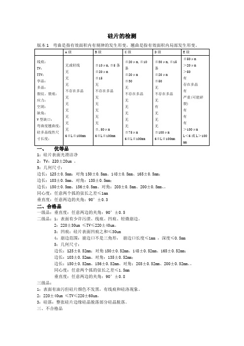
硅片的检测1:硅片表面光滑洁净2:TV:220±20um 。
3:几何尺寸:边长:125±0.5mm;对角150±0.5mm、148±0.5mm、165±0.5mm;边长:103±0.5mm、对角:135±0.5mm;边长:150±0.5mm、156±0.5mm、对角:203±0.5mm、200±0.5mm、。
同心度:任意两个弧的弦长之差≤1mm垂直度:任意两边的夹角:90°±0.3二、合格品一级品:垂直度:任意两边的夹角:90°±0.5二级品:1:表面有少许污渍、线痕。
凹痕、轻微崩边。
2:220±30um ≤TV≤220±40um。
3:凹痕:硅片表面凹痕之和≤30um4:崩边范围:崩边口不是三角形,崩边口长度≤1mm ,深度≤0.5mm 5:几何尺寸:边长:125±0.52mm;对角150±0.52mm、148±0.52mm、165±0.52mm;边长:103±0.52mm、对角:135±0.52mm;边长:150±0.52mm、156±0.52mm、对角:203±0.52mm、200±0.52mm、。
同心度:任意两个弧的弦长之差≤1.5mm垂直度:任意两边的夹角:90°±0.8三级品:1:表面有油污但硅片颜色不发黑,有线痕和硅洛现象。
2:220±40um ≤TV≤220±60um。
3:硅落:整张硅片边缘硅晶脱落部分硅晶脱落。
三、不合格品严重线痕、厚薄片:TV>220±60um。
崩边片:有缺陷但可以改¢103的硅片气孔片:硅片中间有气孔外形片:切方滚圆未能磨出的硅片。
倒角片(同心度):任意两个弧的弦长之差>1.5mm菱形片:(垂直度):任意两边的夹角>90°±0.8凹痕片:硅片两面凹痕之和>30um脏片:硅片表面有严重污渍且发黄发黑尺寸偏差片:几何尺寸超过二级片的范围。
硅片规格说明书

Chapter 1.6I - Substrate SpecificationsPolished Single-Crystal Silicon, Prime Wafers(all numbers nominal)Wafer Specification TableAvailable silicon wafers at NanoLab stockroom are listed in table2, below.Note: NanoLab offers wafers with one major flat (SEMI standard) due to the fact that the majority of our automated equipment are set up to accept wafers with single flat, only (no minor flat).This includes: AMAT Centura, STS, and lam etchers, as well as ASML, GCAWS2 and GCAWS6 steppers in the lab.SEMI standard major flat size is defined as:For 4- inch wafers flat length (mm) = 37.5 (+2.5)For 6-inch wafers flat length (mm) = 57.5 (+2.5)II - Processing Notes1. Class Wafers –A large variety of glasses are available with different metal-oxide contents. Please referto chapter 1.15 MOD 31 for more detail. NanoLab stocks borofloat and fused silica (known as quartz) wafers. You can obtain other type of glass wafers from vendors. Please keep in mind your wafers will need to have single flat (SEMI standard specification) much like regular silicon substrates (above table), if you are going to use them on any of the automated tools in the lab. Wafer flatness may be an issue, if lithography steps are to be done on ASML stepper. This tool requires less than 70 um height variation across a 6-inch wafer, otherwise wafer handling will be a problem on this particular tool. For moreinformation about glass wafer processing follow our chapter 1.15 link at:/labmanual/chap1/1.15processmods.pdf2. Scribing wafers- Members often need to diamond scribe their wafers for identification. Do NOT scribewafers on their back, if you are going to send them through any of the etchers with electrostatic chucks, as well the ASML stepper. The wafer handler on ASML300 stepper cannot handle wafers with deep scratch marks on their back. Best practice is to lightly scribe the top near the flat on your wafers.III - Sorting Unlabeled Silicon WafersThe quality, resistivity type, bulk resistivity, and crystal orientation of unidentified Si wafers can be determined if the wafers are new (unused). The following is a description of the procedures to follow for identifying "unknown" wafers.1. Bright Light Inspection(1) Inspect all wafers under the bright light in V1 (VLSI area).(2) Discard any badly scratched or very hazy wafers.2. Determining Resistivity TypeUse MILLER DESIGN FPP-5000 (4ptprb) to measure resistivity type.(1) Place the wafer, unpolished (dull) side up, over the probe opening.(2) Depress the button (don't touch the wafer with fingers, tweezers, or vacuum wand while testing).(3) N or P for dopant type will be displayed.Consult the manual for VECCO FPP 4-POINT chapter 8.1 for more detailed instruction3. Measuring Bulk ResistivityUse MILLER DESIGN FPP-5000: Please see the instruction posted in Chapter 8.1 and the SLICE option of the tool with proper wafer thickness to be entered under the PRGM mod. Consult the manual for VECCO FPP 4-POINT chapter 8.1 for more detailed instructionDetermine Crystal OrientationUsing a diamond scribe and tweezers, cleave one wafer from each box. This is a destructive method.(1) With a diamond scribe, make a small nick in the wafer at the major flat.(2) Apply pressure to the nicked area with tweezers in order to cleave the wafer.(3) Make another nick in the cleaved piece and repeat step 2.(4) If the cleaved pieces form rectangles (cleave at 90 deg. angles), then the crystal orientation of the Siis <100>. If the cleaved pieces form triangles (cleave diagonally), then the crystal orientation of the Si is <111>.(5) Alternately, flat and secondary flat orientation may be compared to orientation conventions shown inthe Semiconductor Technology Handbook.IV - P-Type 4-inch Wafer Roughness DataThese are AFM images of P-type 4" prime wafers (below). These wafers are very smooth with the RMS roughness of around 2-4 angstroms. For each sample there are two 5 x 5 micron images, one entitled roughness analysis and the other entitled flatten.The samples were cut from 4" p-type prime wafers, and diced by disco saw utilizing a 2-micron sacrificial photoresist layer. After the dicing, samples were washed in acetone, IPA and DI water, then atomic forced microscope (AFM) was used to measure the roughness.V –Trace Elements in 4”and 6” Prime and Test WafersWRS Materials, our supplier of 4” and 6” wafers provided an analy sis of trace elements in their wafers.Application Note:Metals TestingWRS Materials follows SEMI Spec guidelines in all three of our facilities for surface metals testing.Below are the SEMI Spec requirements for surface metals according to SEMI M1 SPECIFICATIONS FOR POLISHED MONOCRYSTALLINE SILICON WAFERS.SEMI Spec RequirementsTable 1: Suggested Polished Wafer Surface Metal Contamination Limits Appropriate to Circuits and Devices with a Minimum Linewidth in the Range of 0.8 – 1.2 µmDue to high measurement variability, data are recorded for process capability and not for individual shipment quality reports.Technique & MethodologyWRS Materials tests these SEMI Spec guidelines by outsourcing wafers to ChemTrace, where the wafers undergo Vapor Phase Decomposition (VPD) inductively coupled plasma – mass spectrometry (ICP-MS).Silicon wafers are placed in a pre-cleaned high purity chamber saturated with Hydrofluoric Acid (HF) vapor. The native or thermal oxide on the silicon wafer is dissolved in the presence of the HF vapor. Metal impurities incorporated into the oxide layer are released and dissolved in the acid during the scanning process.A drop of an ultrapure acid etchant is added to the surface and the analysis area is scanned in a reproducible manner. The scanning solution is then collected for ICP-MS analysis.Table 3: Typical Elements and Detection Limit for Surface Metals Analysis using VPD-ICPMS Method.CapabilitiesCurrently the WRS San Jose, CA facility sends wafers out for trace metal analysis once a week and guarantee a metals spec of <5E10 atoms/cm2 for all metals listed in table 3.。
硅片硅片大全(中英文对照I-Z)

分享举报| 硅片行业术语大全(中英文对照 I-Z)热9徐静文 2009-12-31 15:03硅片行业术语大全(中英文对照 I-Z)硅片行业术语大全(中英文对照 I-Z)In got - A cy lindr icalsolid made of p olycr ystal lineor si nglecryst al si licon from whic h waf ers a re cu t.晶锭 - 由多晶或单晶形成的圆柱体,晶圆片由此切割而成。
L aserLight-Scat terin g Eve nt -A sig nal p ulsethatlocat es su rface impe rfect ionson awafer.激光散射 -由晶圆片表面缺陷引起的脉冲信号。
La y - T he ma in di recti on of surf ace t extur e ona waf er. 层 - 晶圆片表面结构的主要方向。
L ightPoint Defe ct (L PD) (Not p refer red;see l ocali zed l ight-scatt erer)光点缺陷(LPD) (不推荐使用,参见“局部光散射”)Lith ograp hy -The p roces s use d totrans fer p atter ns on to wa fers.光刻- 从掩膜到圆片转移的过程。
Loca lized Ligh t-Sca ttere r - O ne fe ature on t he su rface of a wafe r, su ch as a pi t orascr atchthatscatt ers l ight. It i s als o cal led a ligh t poi nt de fect.局部光散射 -晶圆片表面特征,例如小坑或擦伤导致光线散射,也称为光点缺陷。
硅片平整度知识介绍

STIR
MAX MEAN MIN
0.8 0.6 0.4 0.2 0 A B 厂家 C 有研
上图为各厂家STIR均值中的MAX、MEAN、MIN比较
工艺过程硅片平整度变化
擦片后、一次/牺牲氧化(900C)后、SIN(700C)后采用 光刻PENKIB1设备进行平整度测量,每片的平整度三次测量
2.G为距单元块上每一点截距最小的平面;
3.STIR max= Max( STIR1, STIR2,..., STIR n);
STIR/L- Site(Site Total Indicator Reading)
定义:STIRi /L= | ai |+ | bi | i=1,2,3,4,...,n ( SEMI标准中为SFQR ) 说明: 1.参考平面bf G i为距单元块上每一点截距最小的平面;
Box # MEAN Pre 11/17/05 shipment
1101701 1101877 1101977 1102109 1211559 1212044 1251255 1253532 1257868 1262722 1263180 1263306 1264530 1264754 1272394 1292925 1298844 1299867 1301689
Front
Reference Surface
Back
Reference Plane and Area
Reference Plane and Area
3Point
Reference Plane and Area
Least Squares (site)
Reference Plane and Area
Ideal(全面)
硅片行业术语大全

硅片行业术语大全(中英文对照 I-Z)Ingot - A cylindrical solid made of polycrystalline or single crystal silicon from which wafers are cut.晶锭 - 由多晶或单晶形成的圆柱体,晶圆片由此切割而成。
Laser Light-Scattering Event - A signal pulse that locates surface imperfections on a wafer. 激光散射 - 由晶圆片表面缺陷引起的脉冲信号。
Lay - The main direction of surface texture on a wafer.层 - 晶圆片表面结构的主要方向。
Light Point Defect (LPD) (Not preferred; see localized light-scatterer)光点缺陷(LPD) (不推荐使用,参见“局部光散射”)Lithography - The process used to transfer patterns onto wafers.光刻 - 从掩膜到圆片转移的过程。
Localized Light-Scatterer - One feature on the surface of a wafer, such as a pit or a scratch that scatters light. It is also called a light point defect.局部光散射 - 晶圆片表面特征,例如小坑或擦伤导致光线散射,也称为光点缺陷。
Lot - Wafers of similar sizes and characteristics placed together in a shipment.批次 - 具有相似尺寸和特性的晶圆片一并放置在一个载片器内。
多晶硅片检验标准(185um规格)

A类成品硅片(185um规格)检验标准PAGE (页) :1 OF 2 1、目的为了规范硅片的检验工作,明确硅片检验的项目和检验标准,特制定本文件。
2、范围适用于本公司多晶硅片的分选包装工序。
3、职责品质管理中心:负责对硅片进行检验,确保分选后的硅片等级达到客户的要求。
4、作业内容多晶硅片检验项目和标准类别(Sort)项目(Item)单位(Unit)指标/参数/要求(Index/Parameter/Request)规格尺寸(Dimension)宽度(Width)mm156±0.5mm硅片对角(Wafer Diagonal)mm 219.2±0.5mm倒角(Bevel angle)mm 1.5±0.5mm in 450厚度(Thickness)μm185±15μm(五点厚度平均值)电学性能参数(performance parameter)生长方法(Growth method)定向生长导电类型(Conductivity type)P掺杂剂(Dopant) B电阻率范围(Resistivity)Ω.cm1-3Ω.cm少子寿命(Lifetime)us ≥4us(硅块均值)晶粒大小(Grain Size)Pcs/cm2`≤10 Pcs/cm2碳含量(Carbon concentration)atoms/cm3≤5×1017atoms/cm3氧含量(Oxygen concentration)atoms/cm3≤8×1017atoms/cm3外观质量指标(Surface quality)TTV μm≤30μm 晶介(Micrograin)mm2≥3 mm2线痕(Saw marks)μm≤15μm 边缘角度(Rectangular angle)00900±0.30翘曲度(Warpage)μm≤50μm 裂痕、缺口、穿孔(Crack、Gap、Hole)不允许A类成品硅片(185um规格)检验标准PAGE (页) :2 OF 2小亮边(Tiny Luminance Edge)长度≤硅片边长的1/3,宽度≤片厚的1/3崩边、缺角(Edge chips)mm单面崩边宽度≤0.5 mm;延伸≤0.2mm;每片总数量≤2个,间隔≥30mm(不允许穿透)应力(Stress)摇动无“吧啦”声响表面质量(Surface quality)硅片表面不允许有明显线痕,手感不明显,凹坑,无硅胶残留,表面无沾污和异常斑点。
硅片行业中英文对照
硅片行业术语大全(中英文对照 A—H)Acceptor - An element, such as boron, indium, and gallium used to create a free hole in a semiconductor. The acceptor atoms are required to have one less valenceelectron than the semiconductor.受主 - 一种用来在半导体中形成空穴的元素,比如硼、铟和镓。
受主原子必须比半导体元素少一价电子Alignment Precision - Displacement of patterns that occurs during thephotolithography process.套准精度 - 在光刻工艺中转移图形的精度。
Anisotropic — A process of etching that has very little or no undercutting 各向异性—在蚀刻过程中,只做少量或不做侧向凹刻。
Area Contamination - Any foreign particles or material that are found on the surface of a wafer。
This is viewed as discolored or smudged, and it is the result of stains,fingerprints, water spots, etc.沾污区域 - 任何在晶圆片表面的外来粒子或物质.由沾污、手印和水滴产生的污染。
Azimuth, in Ellipsometry —The angle measured between the plane of incidence andthe major axis of the ellipse.椭圆方位角 - 测量入射面和主晶轴之间的角度。
硅片的等级标准
硅片的检测1:硅片表面光滑洁净2:TV:220±20um 。
3:几何尺寸:边长:125±0.5mm;对角150±0.5mm、148±0.5mm、165±0.5mm;边长:103±0.5mm、对角:135±0.5mm;边长:150±0.5mm、156±0.5mm、对角:203±0.5mm、200±0.5mm、。
同心度:任意两个弧的弦长之差≤1mm垂直度:任意两边的夹角:90°±0.3二、合格品一级品:垂直度:任意两边的夹角:90°±0.5二级品:1:表面有少许污渍、线痕。
凹痕、轻微崩边。
2:220±30um ≤TV≤220±40um。
3:凹痕:硅片表面凹痕之和≤30um4:崩边范围:崩边口不是三角形,崩边口长度≤1mm ,深度≤0.5mm 5:几何尺寸:边长:125±0.52mm;对角150±0.52mm、148±0.52mm、165±0.52mm;边长:103±0.52mm、对角:135±0.52mm;边长:150±0.52mm、156±0.52mm、对角:203±0.52mm、200±0.52mm、。
同心度:任意两个弧的弦长之差≤1.5mm垂直度:任意两边的夹角:90°±0.8三级品:1:表面有油污但硅片颜色不发黑,有线痕和硅洛现象。
2:220±40um ≤TV≤220±60um。
3:硅落:整张硅片边缘硅晶脱落部分硅晶脱落。
三、不合格品严重线痕、厚薄片:TV>220±60um。
崩边片:有缺陷但可以改¢103的硅片气孔片:硅片中间有气孔外形片:切方滚圆未能磨出的硅片。
倒角片(同心度):任意两个弧的弦长之差>1.5mm菱形片:(垂直度):任意两边的夹角>90°±0.8凹痕片:硅片两面凹痕之和>30um脏片:硅片表面有严重污渍且发黄发黑尺寸偏差片:几何尺寸超过二级片的范围。
硅片硅片大全(中英文对照 I-Z)
Laser Light-Scattering Event - A signal pulse that locates surface imperfections on a wafer.
激光散射 - 由晶圆片表面缺陷引起的脉冲信号。
Lay - The main direction of surface texture on a wafer.
层 - 晶圆片表面结构的主要方向。
Light Point Defect (LPD) (Not preferred; see localized light-scatterer)
光点缺陷(LPD) (不推荐使用,参见“局部光散射”)
Lithography - The process used to transfer patterns onto wafers.
条痕 - 螺纹上的缺陷或污染。
Subsite, of a Site - An area found within the site, also rectangular. The center of the subsite must be located within the original site.
最小条件或方向 - 确定晶圆片是否合格的允许条件。
Minority Carrier - A carrier, either a hole or an electron that is not dominant in a specific region, such as electrons in a P-Type area.
Miller索指数 - 三个整数,用于确定某个并行面。这些整数是来自相同系统的基本向量。
硅片行业术语大全

Crater - Visible under diffused illumination, a surface imperfection on a wafer that can be distinguished individually. pv001·net
微坑 - 在扩散照明下可见的,晶圆片表面可区分的缺陷。
Conductivity (electrical) - A measurement of how easily charge carriers can flow throughout a material. pv001·net
传导性(电学方面) - 一种关于载流子通过物质难易度的测量指标 。 pv001·net
沾污区域 - 任何在晶圆片表面的外来粒子或物质。由沾污、手印和水滴产生的污染。 中国光伏材料设备网
Azimuth, in Ellipsometry - The angle measured between the plane of incidence and the major axis of the ellipse.
搀杂剂 - 可以为传导过程提供电子或空穴的元素,此元素可以改变传导特性。晶圆片 搀杂
剂可以在元素周期表的 III 和 V 族元素中发现。
Doping - The process of the donation of an electron or hole to the conduction process(CMP) - 平整和抛光晶圆片的工艺,采用化学移除和机械抛光两种方式。 此工艺在前道工艺中使用。 pv001·net
Chuck Mark - A mark found on either surface of a wafer, caused by either a robotic end effector, a chuck, or a wand. 光伏材料设备网
硅片行业术语大全(中英文对照+I-Z)
硅片行业术语大全(中英文对照I-Z)Ingot - A cylindrical solid made of polycrystalline or single crystal silicon from which wafers are cut.晶锭- 由多晶或单晶形成的圆柱体,晶圆片由此切割而成。
Laser Light-Scattering Event - A signal pulse that locates surface imperfections on a wafer.激光散射- 由晶圆片表面缺陷引起的脉冲信号。
Lay - The main direction of surface texture on a wafer.层- 晶圆片表面结构的主要方向。
Light Point Defect (LPD) (Not preferred; see localized light-scatterer)光点缺陷(LPD) (不推荐使用,参见“局部光散射”)Lithography - The process used to transfer patterns onto wafers.光刻- 从掩膜到圆片转移的过程。
Localized Light-Scatterer - One feature on the surface of a wafer, such as a pit or a scratch that scatters light. It is also called a light point defect.局部光散射- 晶圆片表面特征,例如小坑或擦伤导致光线散射,也称为光点缺陷。
Lot - Wafers of similar sizes and characteristics placed together in a shipment.批次- 具有相似尺寸和特性的晶圆片一并放置在一个载片器内。
硅片行业术语大全中英文对照I-Z

硅片行业术语大全(中英文对照 I—Z)Ingot — A cylindrical solid made of polycrystalline or single crystal silicon from which wafer s are cut。
晶锭—由多晶或单晶形成的圆柱体,晶圆片由此切割而成.Laser Light—Scattering Event — A signal pulse that locates surface imperfections on a wafer。
激光散射 - 由晶圆片表面缺陷引起的脉冲信号。
Lay — The main direction of surface texture on a wafer。
层—晶圆片表面结构的主要方向。
Light Point Defect (LPD)(Not preferred; see localized light-scatterer) 光点缺陷(LPD)(不推荐使用,参见“局部光散射")Lithography — The process used to transfer patterns onto wafer s.光刻—从掩膜到圆片转移的过程。
Localized Light—Scatterer —One feature on the surface of a wafer, such as a pit or a scratch that scatters light. It is also called a light point defect。
局部光散射—晶圆片表面特征,例如小坑或擦伤导致光线散射,也称为光点缺陷。
Lot —Wafer s of similar sizes and characteristics placed together in a shipment。
批次—具有相似尺寸和特性的晶圆片一并放置在一个载片器内.Majority Carrier - A carrier, either a hole or an electron that is dominant in a specific region, such as electrons in an N—Type area。
硅片专业术语
硅片专业术语Acceptor - An element, such as boron, indium, and gallium used to create a free hole in a semiconductor. The acceptor atoms are required to have one less valence electron than the semiconductor.受主- 一种用来在半导体中形成空穴的元素,比如硼、铟和镓。
受主原子必须比半导体元素少一价电子Alignment Precision - Displacement of patterns that occurs during the photolithography process.套准精度 - 在光刻工艺中转移图形的精度。
Anisotropic - A process of etching that has very little or no undercutting各向异性 - 在蚀刻过程中,只做少量或不做侧向凹刻。
Area Contamination - Any foreign particles or material that are found on the surface of a wafer. This is viewed as discolored or smudged, and it is the result of stains, fingerprints, water spots, etc.沾污区域 - 任何在晶圆片表面的外来粒子或物质。
由沾污、手印和水滴产生的污染。
Azimuth, in Ellipsometry - The angle measured between the plane of incidence and the major axis of the ellipse.椭圆方位角- 测量入射面和主晶轴之间的角度。
硅片的等级标准

硅片的检测1:硅片表面光滑洁净2:TV:220±20um 。
3:几何尺寸:边长:125±0.5mm;对角150±0.5mm、148±0.5mm、165±0.5mm;边长:103±0.5mm、对角:135±0.5mm;边长:150±0.5mm、156±0.5mm、对角:203±0.5mm、200±0.5mm、。
同心度:任意两个弧的弦长之差≤1mm垂直度:任意两边的夹角:90°±0.3二、合格品一级品:垂直度:任意两边的夹角:90°±0.5二级品:1:表面有少许污渍、线痕。
凹痕、轻微崩边。
2:220±30um ≤TV≤220±40um。
3:凹痕:硅片表面凹痕之和≤30um4:崩边范围:崩边口不是三角形,崩边口长度≤1mm ,深度≤0.5mm 5:几何尺寸:边长:125±0.52mm;对角150±0.52mm、148±0.52mm、165±0.52mm;边长:103±0.52mm、对角:135±0.52mm;边长:150±0.52mm、156±0.52mm、对角:203±0.52mm、200±0.52mm、。
同心度:任意两个弧的弦长之差≤1.5mm垂直度:任意两边的夹角:90°±0.8三级品:1:表面有油污但硅片颜色不发黑,有线痕和硅洛现象。
2:220±40um ≤TV≤220±60um。
3:硅落:整张硅片边缘硅晶脱落部分硅晶脱落。
三、不合格品严重线痕、厚薄片:TV>220±60um。
崩边片:有缺陷但可以改¢103的硅片气孔片:硅片中间有气孔外形片:切方滚圆未能磨出的硅片。
倒角片(同心度):任意两个弧的弦长之差>1.5mm菱形片:(垂直度):任意两边的夹角>90°±0.8凹痕片:硅片两面凹痕之和>30um脏片:硅片表面有严重污渍且发黄发黑尺寸偏差片:几何尺寸超过二级片的范围。
硅片的等级标准
硅片的检测1:硅片表面光滑洁净2:TV:220±20um 。
3:几何尺寸:边长:125±0.5mm;对角150±0.5mm、148±0.5mm、165±0.5mm;边长:103±0.5mm、对角:135±0.5mm;边长:150±0.5mm、156±0.5mm、对角:203±0.5mm、200±0.5mm、。
同心度:任意两个弧的弦长之差≤1mm垂直度:任意两边的夹角:90°±0.3二、合格品一级品:垂直度:任意两边的夹角:90°±0.5二级品:1:表面有少许污渍、线痕。
凹痕、轻微崩边。
2:220±30um ≤TV≤220±40um。
3:凹痕:硅片表面凹痕之和≤30um4:崩边范围:崩边口不是三角形,崩边口长度≤1mm ,深度≤0.5mm 5:几何尺寸:边长:125±0.52mm;对角150±0.52mm、148±0.52mm、165±0.52mm;边长:103±0.52mm、对角:135±0.52mm;边长:150±0.52mm、156±0.52mm、对角:203±0.52mm、200±0.52mm、。
同心度:任意两个弧的弦长之差≤1.5mm垂直度:任意两边的夹角:90°±0.8三级品:1:表面有油污但硅片颜色不发黑,有线痕和硅洛现象。
2:220±40um ≤TV≤220±60um。
3:硅落:整张硅片边缘硅晶脱落部分硅晶脱落。
三、不合格品严重线痕、厚薄片:TV>220±60um。
崩边片:有缺陷但可以改¢103的硅片气孔片:硅片中间有气孔外形片:切方滚圆未能磨出的硅片。
倒角片(同心度):任意两个弧的弦长之差>1.5mm菱形片:(垂直度):任意两边的夹角>90°±0.8凹痕片:硅片两面凹痕之和>30um脏片:硅片表面有严重污渍且发黄发黑尺寸偏差片:几何尺寸超过二级片的范围。