最详细的PM66芯片使用手册20131214
ICMF062P250MFR Common Mode Filter 数据手册说明书
4. 1 PART NUMBER CODE ICMF 06 2P 250 M F R ① ② ③ ④ ⑤⑥ ⑦
① Series name of ICT’s Common Mode Filter ② Dimensions, 0.87mm (L) ⅹ 0.67mm (W) ③ The Number of lines, 2P = 2 lines ④ Common Mode Impedance (at 100MHz), 25 ⅹ 100= 25Ω ⑤ Tolerance of common mode impedance, M= ±25% ⑥ Type of electrode plating: F= Lead Free ⑦ Packing Type, R= Reel
3. APPLICATIONS
• LVDS lines in notebook computers • USB2.0, IEEE1394, DVI, HDMI lines in PDP, LCD TV, DVD Player, PC, Audio player, DSC • MDDI, MIPI in mobile phone
4028
750
3230
325
3768
490
4038
760
L-box + 10S-box 380 x 370 x 200
Total(g) Chip(g)
6147 7503 8043 6177 7523 8063
620 960 1500 650 980 1520
<PQ Box>
Packing box + Product weight
Product CMF CMEF
SUSS PM5 手动芯片探测系统说明书
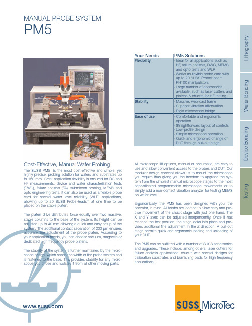
L i t h o g r a p h y W a f e r B o n d i n gD e v i c e B o n d i n g T e s t i n g MANUAL PROBE SYSTEMPM5Cost-Effective, Manual Wafer ProbingThe SUSS PM 5 is the most cost-effective and simple, yet highly precise, probing solution for wafers and substrates up to 150 mm. Great application flexibility is ensured for DC and HF measurements, device and wafer characterization tests (DWC), failure analysis (FA), submicron probing, M EM S and opto engineering tests. It can also be used as a flexible probe card for special wafer level reliability (WLR) applications, allowing up to 20 SUSS ProbeHeads TM at one time to be placed on the stable platen.The platen drive distributes force equally over two massive,All microscope lift options, manual or pneumatic, are easy to use and allow convenient access to the probes and DUT. Our modular design concept allows us to mount the microscope you require thus giving you the freedom to upgrade the sys-tem from the simplest manual microscope stages to the most sophisticated programmable microscope movements or to simply add a non-contact vibration analyzer for testing MEMS on wafer level.Ergonomically, the PM 5 has been designed with you, the operator, in mind. All knobs are located to allow easy and pre-cise movement of the chuck stage with just one hand. The X and Y axes can be adjusted independently. Once it has reached the test position, the stage locks into place and pro-vides additional fine adjustment in the Z direction. A pull-out stage permits quick and ergonomic loading and unloading of your DUT.The PM5 can be outfitted with a number of SUSS accessories and upgrades. These include, among others, laser cutters for failure analysis applications, chucks with special designs for calibration substrates and burnishing pads for high frequency applications.Technical Data: PM5 Manual Probe StationSUSS MicroTec Test Systems Worldwide Contacts: SUSS MicroTec Test Systems+49-35240-730 SUSS MicroTec China+86-21-5234-0432Design verification with SUSS PM5 MEMS testing with SUSS PM5and Polytec MSA 400Testing HF on PM5 (for small budgets).Dresden .Hsin-Chu .Munich .Saint Je oire.Santa Clara .Shanghai .Te mpe.Vaihinge n .Wate rbury Ce nte r .Yokohama。
mGreen 芯片模组说明书

mGreen 芯片模组使用说明书C2C Link 公司Jan Jan..02,201201221.简介mGreen 芯片模组是用来产生532-nm 绿光的单一组件。
采用808-nm 半导体激光器(LD )直接泵浦mGreen 芯片模组的简单结构,即可轻松获得500-1000mW 的绿光输出。
2.mGreen 芯片模组介绍如图1所示,mGreen 芯片模组由4个部件组成:硅基片,掺杂浓度为1%的Nd:YVO 4晶体,掺杂浓度为5mol%的MgO:PPLN 晶体和铜盖。
Nd:YVO 4晶体和MgO:PPLN 晶体经高精度准直固定在硅基片上,因此两个晶体的通光面严格平行。
Nd:YVO 4晶体和MgO:PPLN 晶体的光轴准直于竖直方向。
Nd:YVO 4晶体的入射面镀膜为HT@808nm ,HR@1064nm &532nm 。
MgO:PPLN 晶体的出射面镀膜为HR@1064nm ,HT@532nm 。
mGreen 芯片模组的尺寸为7(长)×4.5(宽)×2(厚)mm 3(即体积为0.063cm 3)。
图1.mGreen 芯片模组的3D 视图3.基于mGreen 芯片模组的绿光激光器结构采用mGreen 芯片模组制作激光器(laser head ),最基本的配置需求是一个硅基片MgO:PPLN 晶体Nd:YVO 4晶体铜盖作为泵浦源的808-nm 半导体激光器(c-mount 或者F-mount ),一个mGreen 芯片模组和相关配件(如半导体制冷片,热敏电阻和金属结构件等)。
图2给出了基于mGreen 芯片模组,808-nm 半导体激光器(c-mount )作为泵浦源的绿光激光器3D 视图。
值得注意的是,1.为了获得mGreen 芯片模组的最佳性能,对于偏振态为TE 的808-nm 半导体激光器需要旋转90度;2.mGreen 芯片模组的硅基片需要和热沉或半导体制冷片接触良好,以确保满足激光器工作要求的散热条件;3.mGreen 芯片模组同808-nm 半导体激光器之间的距离约为1mm ;4.无需聚焦镜和输出耦合镜;5.为保证较好的光束质量和功率转换效率,最好采用带快轴整形的808-nm 半导体激光器作为泵浦源,其光束在水平和竖直两个方向的发散角约为7度,光斑为方形。
最详细的PM66芯片使用手册20131214
描述 触収输入引脚(低有效)
输出引脚 接喇叭两端
电源正端 电源地 系统复位端(低有效) 编程控制端
-5-
PM66DATASHEET
2 PM66 的典型应用电路及 MCU 控制方式
2.1 典型线路
图 1 并行按键模式,PWM* 音频输出方式接线图
6K
32 100 200 400 800 1600 3200
8K
24 75 150 300 600 1200 2400
10K
19.2 60 120 240 480 960 1920
12K
16 50 100 200 400 800 1600
16K
12 37.5 75 150 300 600 1200
20K
4.3.1 关于静音(MUTE)的使用.................................................................................................. - 23 4.3.2 关于 Group <<组>>的应用.................................................................................................... - 24 5. FAQ ...................................................................................................................................................... - 26 -
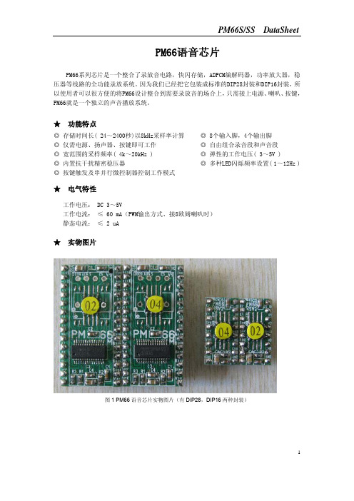
PM66语音芯片资料
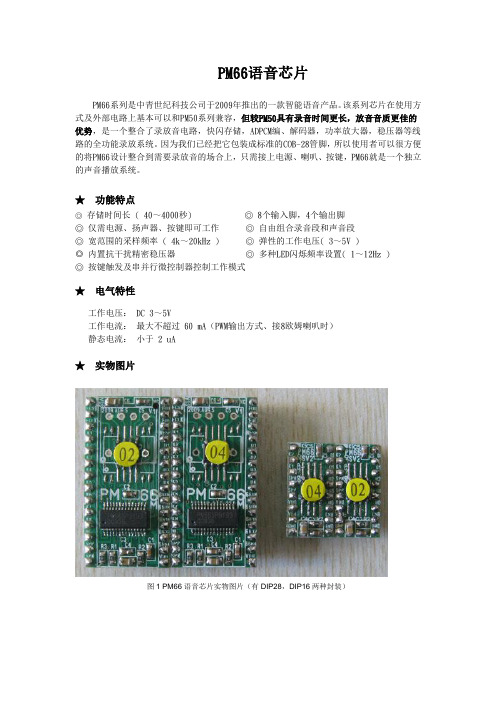
PM66语音芯片PM66系列是中青世纪科技公司于2009年推出的一款智能语音产品。
该系列芯片在使用方式及外部电路上基本可以和PM50系列兼容,但较PM50具有录音时间更长,放音音质更佳的优势,是一个整合了录放音电路,快闪存储,ADPCM编、解码器,功率放大器,稳压器等线路的全功能录放系统。
因为我们已经把它包装成标准的COB-28管脚,所以使用者可以很方便的将PM66设计整合到需要录放音的场合上,只需接上电源、喇叭、按键,PM66就是一个独立的声音播放系统。
★功能特点◎存储时间长 ( 40~4000秒) ◎ 8个输入脚,4个输出脚◎ 仅需电源、扬声器、按键即可工作◎ 自由组合录音段和声音段◎ 宽范围的采样频率 ( 4k~20kHz ) ◎ 弹性的工作电压( 3~5V )◎内置抗干扰精密稳压器◎ 多种LED闪烁频率设置( 1~12Hz )◎ 按键触发及串并行微控制器控制工作模式★电气特性工作电压: DC 3~5V工作电流:最大不超过 60 mA(PWM输出方式、接8欧姆喇叭时)静态电流:小于 2 uA★实物图片图1 PM66语音芯片实物图片(有DIP28,DIP16两种封装)图2 PM66编程器实物图1 PM66语音芯片型号及引脚定义(1)PM66系列按照录音时间区分,共有6种产品型号,下表为各种型号在不同的采样频率下可存放的时间对照表。
(2)PM66引脚定义及实际图片2 PM66的典型应用电路及控制方式(1)、并行模式、按键操作在PM66系列芯片的并行控制方式下可以分8段语音录放,K1~K8脚可以分别触发与其对应的8段语音(低有效),在烧录芯片的时候,可以设置为下降沿触发或者低电平触发。
K1~K8端口有内置上拉电阻和防抖动设计,可直接外接按键来触发放音。
也可用单片机口线直接对其操作。
如图1:图1 并行按键模式,PMW音频输出方式接线图连接扬声器的两种方式(PWM和DAC)音频输出方式的选择,首先需要在编程软件中设定,烧写芯片后按照以下说明连接。
优利德 UPO1204X-E系列数据手册 说明书
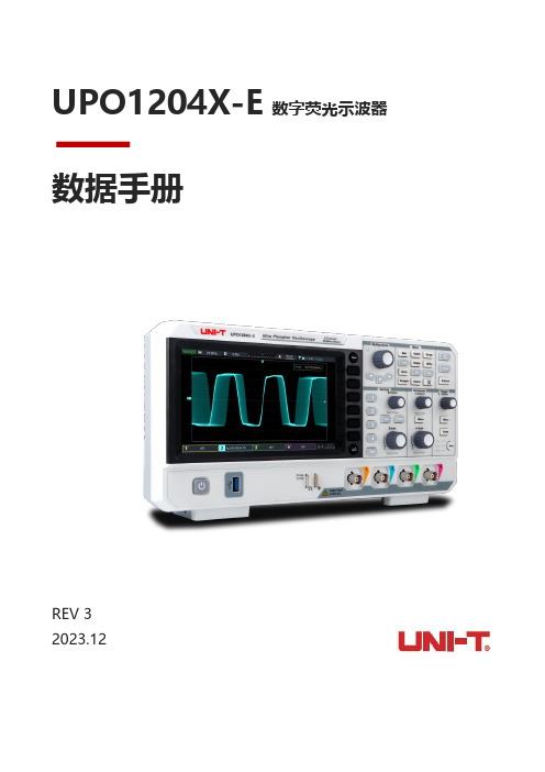
UPO1204X-E数字荧光示波器数据手册REV32023.12⏹模拟通道带宽:200MHz⏹模拟通道数:4⏹最大采样率:2GSa/s⏹垂直档位:500μV/div-20V/div⏹低底噪声:<100μVrms⏹最大存储深度可达28Mpts⏹波形捕获率最高300,000wfms/s⏹硬件实时波形不间断录制60,000帧⏹可自动测量36种波形参数,测量范围可选:屏幕或光标区域⏹支持7位硬件频率计测量⏹DVM支持交直流真有效值测量⏹波形运算功能(FFT、加、减、乘、除、数字滤波、逻辑运算和高级运算)⏹1M点增强FFT功能,支持频率设置,瀑布图,检波设置和标记测量等⏹丰富的触发功能(边沿,脉宽,视频,斜率,欠幅脉冲,超幅脉冲,延迟,超时,持续时间,建立保持、第N边沿和码型触发)⏹标配RS232、I2C、SPI触发⏹标配RS232、I2C、SPI全内存硬件实时解码⏹Ultra Phosphor超级荧光显示效果,高达256级的灰度显示⏹7英寸WVGA(800×480)TFT液晶屏⏹丰富的接口:USB Host、USB Device、LAN、EXT Trig、AUX Out(Trig Out、Pass/Fail、DVM)⏹支持波形导航、标记、段⏹支持SCPI可编程仪器标准命令⏹支持WEB访问和控制UPO1204X-E数字示波器采用了UNI-T新创的数字三维技术Ultra Phosphor2.0,全新外观升级,可实现深存储,高波形捕获率,实时波形录制与回放,256级灰度显示等功能;该款配置200MHz带宽,实时采样率高达2GSa/s,标配4通道,标配最大存储深度28Mpts,Fast Acquire模式下最高可达300,000wfms/s,硬件实时波形不间断录制和波形分析功能最大达6万帧波形;支持DVM模块,拥有丰富的触发和总线解码功能,并支持全内存硬件实时解码;广泛应用包括通信,半导体,计算机,集成电路设计,仪器仪表,工业电子,消费电子,汽车电子,现场维修,研发/教育等众多领域。
PMK 8 PMK 6 PMK 3 快速启动向导说明书
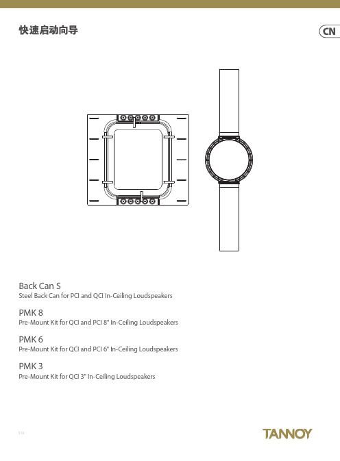
Back Can SSteel Back Can for PCI and QCI In-Ceiling Loudspeakers PMK 8Pre-Mount Kit for QCI and PCI 8" In-Ceiling Loudspeakers PMK 6Pre-Mount Kit for QCI and PCI 6" In-Ceiling Loudspeakers PMK 3Pre-Mount Kit for QCI 3" In-Ceiling LoudspeakersV 1.0带有此标志的终端设备具有强大的电流, 存在触电危险。
仅限使用带有 ¼'' TS 或扭锁式插头的高品质专业扬声器线。
所有的安装或调整均须由合格的专业人员进行。
此标志提醒您, 产品内存在未绝缘的危险电压, 有触电危险。
此标志提醒您查阅所附的重要的使用及维修说明。
请阅读有关手册。
小心为避免触电危险, 请勿打开机顶盖 (或背面挡板)。
设备内没有可供用户维修使用的部件。
请将维修事项交由合格的专业人员进行。
小心为避免着火或触电危险, 请勿将此设备置于雨淋或潮湿中。
此设备也不可受液体滴溅, 盛有液体的容器也不可置于其上, 如花瓶等。
小心维修说明仅是给合格的专业维修人员使用的。
为避免触电危险, 除了使用说明书提到的以外, 请勿进行任何其它维修。
所有维修均须由合格的专业人员进行。
1. 请阅读这些说明。
2. 请妥善保存这些说明。
3. 请注意所有的警示。
4. 请遵守所有的说明。
5. 请勿在靠近水的地方使用本产品。
6. 请用干布清洁本产品。
7. 请勿堵塞通风口。
安装本产品时请遵照厂家的说明。
8. 请勿将本产品安装在热源附近,如 暖 气 片, 炉子或其它产生热量的设备( 包 括功放器)。
9. 请勿移除极性插头或接地插头的安全装置。
接地插头是由两个插塞接点及一个接地头构成。
ST PM6611N 数据手册
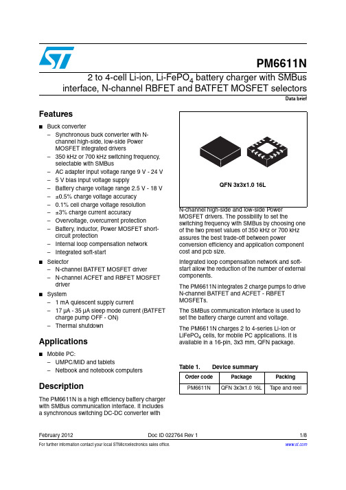
Data briefFor further information contact your local STMicroelectronics sales office.February 2012Doc ID 022764 Rev 11/8PM6611N2 to 4-cell Li-ion, Li-FePO 4 battery charger with SMBus interface, N-channel RBFET and BATFET MOSFET selectorsFeatures■Buck converter–Synchronous buck converter with N-channel high-side, low-side Power MOSFET integrated drivers–350 kHz or 700 kHz switching frequency, selectable with SMBus–AC adapter input voltage range 9 V - 24 V – 5 V bias input voltage supply–Battery charge voltage range 2.5 V - 18 V –±0.5% charge voltage accuracy –0.1% cell charge voltage resolution –±3% charge current accuracy–Overvoltage, overcurrent protection–Battery, inductor, Power MOSFET short- circuit protection–Internal loop compensation network –Integrated soft-start■Selector–N-channel BATFET MOSFET driver–N-channel ACFET and RBFET MOSFET driver ■System– 1 mA quiescent supply current–17 µA - 35 µA sleep mode current (BATFET charge pump OFF - ON)–Thermal shutdownApplications■Mobile PC:–UMPC/MID and tablets–Netbook and notebook computersDescriptionThe PM6611N is a high efficiency battery charger with SMBus communication interface. It includes a synchronous switching DC-DC converter withMOSFET drivers. The possibility to set theswitching frequency with SMBus by choosing one of the two preset values of 350 kHz or 700 kHz assures the best trade-off between powerconversion efficiency and application component cost and pcb size.Integrated loop compensation network and soft-start allow the reduction of the number of external components.The PM6611N integrates 2 charge pumps to drive N-channel BATFET and ACFET - RBFET MOSFETs.The SMBus communication interface is used to set the battery charge current and voltage. The PM6611N charges 2 to 4-series Li-Ion or LiFePO 4 cells, for mobile PC applications. It is available in a 16-pin, 3x3 mm, QFN package.Table 1.Device summaryOrder codePackage Packing PM6611NQFN 3x3x1.0 16LTape and reelTypical application circuitPM6611N2/8Doc ID 022764 Rev 11 Typical application circuitPM6611N Device pinoutDoc ID 022764 Rev 13/82 Device pinoutPackage mechanical data PM6611N 3 Package mechanical dataIn order to meet environmental requirements, ST offers these devices in different grades ofECOP ACK® packages, depending on their level of environmental compliance. ECOPACKspecifications, grade definitions and product status are available at: . ECOPACKis an ST trademark.Table 2.QFN 3x3x1.0 16L mechanical datamm.Dim.Min.Typ.Max.A0.800.90 1.00A10.020.05A20.65 1.00A30.20b0.180.250.30D 2.85 3.00 3.15D1 1.50D2See T able3E 2.85 3.00 3.15E1 1.50E2See T able3e0.450.500.55L0.300.400.50ddd0.08Table 3.Exposed pad variationD2E2VariationMin.Typ.Max.Min.Typ.Min.A0.95 1.10 1.250.95 1.10 1.25B 1.45 1.60 1.75 1.45 1.60 1.754/8Doc ID 022764 Rev 1PM6611N Package mechanical dataDoc ID 022764 Rev 15/8Package mechanical data PM6611N6/8Doc ID 022764 Rev 1PM6611N Revision historyDoc ID 022764 Rev 17/84 Revision historyTable 4.Document revision historyDate RevisionChanges01-Feb-20121Initial release.PM6611NPlease Read Carefully:Information in this document is provided solely in connection with ST products. STMicroelectronics NV and its subsidiaries (“ST”) reserve the right to make changes, corrections, modifications or improvements, to this document, and the products and services described herein at any time, without notice.All ST products are sold pursuant to ST’s terms and conditions of sale.Purchasers are solely responsible for the choice, selection and use of the ST products and services described herein, and ST assumes no liability whatsoever relating to the choice, selection or use of the ST products and services described herein.No license, express or implied, by estoppel or otherwise, to any intellectual property rights is granted under this document. If any part of this document refers to any third party products or services it shall not be deemed a license grant by ST for the use of such third party products or services, or any intellectual property contained therein or considered as a warranty covering the use in any manner whatsoever of such third party products or services or any intellectual property contained therein.UNLESS OTHERWISE SET FORTH IN ST’S TERMS AND CONDITIONS OF SALE ST DISCLAIMS ANY EXPRESS OR IMPLIED WARRANTY WITH RESPECT TO THE USE AND/OR SALE OF ST PRODUCTS INCLUDING WITHOUT LIMITATION IMPLIED WARRANTIES OF MERCHANTABILITY, FITNESS FOR A PARTICULAR PURPOSE (AND THEIR EQUIVALENTS UNDER THE LAWS OF ANY JURISDICTION), OR INFRINGEMENT OF ANY PATENT, COPYRIGHT OR OTHER INTELLECTUAL PROPERTY RIGHT. UNLESS EXPRESSLY APPROVED IN WRITING BY TWO AUTHORIZED ST REPRESENTATIVES, ST PRODUCTS ARE NOT RECOMMENDED, AUTHORIZED OR WARRANTED FOR USE IN MILITARY, AIR CRAFT, SPACE, LIFE SAVING, OR LIFE SUSTAINING APPLICATIONS, NOR IN PRODUCTS OR SYSTEMS WHERE FAILURE OR MALFUNCTION MAY RESULT IN PERSONAL INJURY, DEATH, OR SEVERE PROPERTY OR ENVIRONMENTAL DAMAGE. ST PRODUCTS WHICH ARE NOT SPECIFIED AS "AUTOMOTIVE GRADE" MAY ONLY BE USED IN AUTOMOTIVE APPLICATIONS AT USER’S OWN RISK.Resale of ST products with provisions different from the statements and/or technical features set forth in this document shall immediately void any warranty granted by ST for the ST product or service described herein and shall not create or extend in any manner whatsoever, any liability of ST.ST and the ST logo are trademarks or registered trademarks of ST in various countries.Information in this document supersedes and replaces all information previously supplied.The ST logo is a registered trademark of STMicroelectronics. All other names are the property of their respective owners.© 2012 STMicroelectronics - All rights reservedSTMicroelectronics group of companiesAustralia - Belgium - Brazil - Canada - China - Czech Republic - Finland - France - Germany - Hong Kong - India - Israel - Italy - Japan - Malaysia - Malta - Morocco - Philippines - Singapore - Spain - Sweden - Switzerland - United Kingdom - United States of America8/8Doc ID 022764 Rev 1。
PM66芯片使用手册及参数
K1 = 1; } else {
K1 = 0; } k1_data = k1_data>>1; delay_1(76); K2 = 1; delay_1(76);//发码频率(500HZ) } K1 = 1; } //***************主程序***************// void main (void) { uchar address; P2 = 0xff; while(1) { for (address=0x00; address<0x04; address++) {
PM6632
1000 800 600 480 400 300 240
PM6664
2000 1600 1200 960 800 600 480 1920 1600 1200 960
(2)PM66 引脚定义及实际图片
2
PM66S/SS DataSheet
引脚名称
B、DAC 方式:(示意图以三极管 8050 作为放大器件,用户可根据实际功率需求自行选 择功放器件)。 PM66S/PM66SS 芯片接线图如下图 2
图 2 并行按键模式,DAC 音频输出方式接线图 5
PM66S/SS DataSheet
C、 PM66+LM386 的典型电路(PM66 选用 DAC 模式输出)
⑸、 运行状态显示框
显示的内容:PM66 芯片的型号、载入或保存档案是否成功的提示、芯片烧写进度及故障信息提示。
⑹、 触发模式选项
PM66 芯片的触发模式:按键模式、串列位址(串行地址)模式及并列位址(并行地址)模式。(其它
三种模式为客户定制无需选择)
ProfometerPM-600说明书
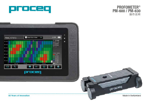
图 2: 测量范围和精度
© 2014 Proceq SA
7
2.4 分辨率
对钢筋的最小间距有所限制,具体取决于保护层深度和钢筋直径。超过
这些限制的钢筋无法区分。
C [英寸][毫米]
8 200
7 180
160 6
140 5
120
4 100
3 80
C S
点检探头范围
大范围
Ø 40 mm Ø 26 mm
Ø 16 mm Ø 12 mm Ø 8 mm
1.1 通用信息........................................... 6 1.2 责任............................................... 6 1.3 安全说明........................................... 6 1.4 正确使用........................................... 6
mark6使用手册
第二章MARK VI控制系统1、系统概貌本厂采用三重冗余型(TMR)结构的MARK VI控制盘,由3套微处理机模块组成,分别是<R><S><T>三台控制处理机、HMI人机接口、<P>保护处理机和输入模块。
MARK VI在<R><S><T>控制模块分别都有专门的通讯卡件VCMI。
由通讯卡件完全数据交换网络的通讯交换和数据表决。
并把数据传送到主处理卡UCVX。
轮控盘的各个模块却分别配备了独立的电源。
特别对于保护模块的<X><Y><Z>三重冗余也配备了三个独立电源,以期提高可靠性。
主控制器包括了<R><S><T>控制模块。
它完成控制、保护和监视的功能。
备用保护包括了<X><Y><Z>,它完成紧急超建和同期检查的保护功能。
无论是输入输出网(Ionet)还是和人机接口HMI的通讯均采用以太网实现。
后者采用了GE公司的UDH(机组数据总线)。
人机接口的软件支持使用了WINDOWS NT 操作系统和CIMPLICITY的图形显示系统。
整个MARK VI系统和DCS的通讯可以采用多种方式。
即可以采用RS232 MODBUS通讯,以这种方式通讯MARK VI可以作为从站也可以作为主站方式。
第二种方式用以太网TCP—IP MODBUS协议通讯,它作为从站进行设置。
第三种方式为以太网TCP—IP GSM方式。
该通讯网络称之为PDH(电厂数据总线)。
无论是UDH和PDH一般都采用双重冗余方式来保证通讯的可靠性。
MARK VI系统的组态见下图。
1.1 硬件配置控制模块<R><S><T>都采用了21槽口标准的UME型机架。
机柜的中心部分自上而下分别为<P><R><S>和<T>。
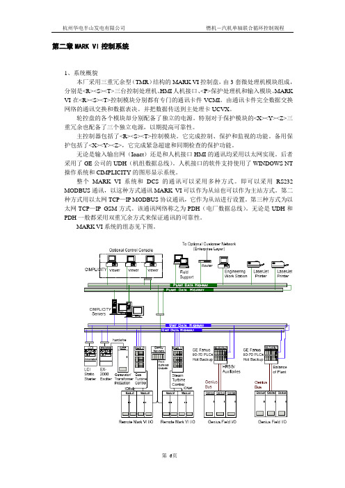
M37160M8和M61266贴片集成电路引脚功能
M37160M8和M61266贴片集成电路引脚功能M37160-11 P11 输入口检测此脚为低时说明S端子输入 52 PWM0 14bit VS控制 1.53 引脚符号功能直流电压(V)4 PWM2 PWM音量控制5 PWM3/P03输出口重低音控制6 PWM4 PWM音量控制7 AD3 AFT IN。
2.38 空0.79 P07 输入口遥控接收。
510 P20 输入口 PROTECT 低电平保护。
511 P21 输入口 X-RAY 高电平保护。
012 AD7 本地键接收。
513 P23 输入口 FACTORY 为低时由外部白平衡仪控制解码与EEPROM 514 P24 输出口静音脚,高电平时静音015 P25 输入口选择不同的工厂密码。
516 P26 输出口 AV控制17 P27输出口AV控制 TV: P26 = 0 P27 = 0 AV1:P26 = 0 P27 = 1 AV2/YC P26 = 1 P27 = 1 YUV: P26 = 1 P27 = 118 CNVss 地019 Xin 地020 Xout 地 521 Vss 地0M37160-222 VCC 电源 523 FILT 时钟滤波 1.624 P37 空脚 0.925 P36 空脚 0.826 P35 空脚 0.827 RESET CUP复位脚 528 FSCIN 时钟输入 229 P15 输出口待机控制开机时输出高电平待机时输出低电平530 SCL3 数据总线。
3.531 SDA3 时钟总线。
3.732 CLK CONT 时钟控制脚,开机时输出高电平。
533 OUT FAST BLANK 534 R R输出035 G G输出036 B B输出037 V SYNC V SYNC 输入 4.838 H SYNC H SYNV输入 4.939 AD8 MONITOR 输入 4.240 P14 输出口 VS 波段控制 VHFL时为高41 P13输出口VS 波段控制 VHFH时为高42 P12输出口VS 波段控制 UHF时为高M61260/M61264/M61266-------1引脚符号功能直流电压(V)1 V RAMP CAP 场锯齿波 3.02 AFT OUT 自动频率控制输出 1.653 VIF VCC +5V 54 SIF VCC +5V 55 V-DRIV 场驱动输出 2.976 V-FB 场反馈 3.677 H-PLL 行锁相环 3.538 DEF GND 地09 LOGIC GDN 地010 FBT IN 行逆程脉冲输入0.811 H-DRE 行驱动输出 2.312 DEF VCC +8V 8.113 VDD OUT (NC) VDD供电滤波 514 R OUT 红色输出 2.515 G OUT 绿色输出 2.316 B OUT 蓝色输出 2.117 H-VCO 行VCO18 MONITOR 管理控制 319 HSYC 行同步 1.220 VSYC 场同步 4.921 B IN 字符蓝色输入22 G IN 字符绿色输入23 R IN 字符红色输入24 FB-IN 字符消隐输入25 CLK CONT 时钟控制 526 SDA IIC总线数据控制 3.827 SCL IIC总线时钟控制 3.528 STANBAY 待机控制 529 CLK OUT 时钟输出 3.3730 RESET 复位 531 CVBS OUT 复合视频信号输出 2.432 MCU 5.7V OUT 微处理器5.7V供电输出 5.63 M61260/M61264/M61266-------233 ABL 自动亮度控制 2.534 XTAL 晶体振荡 3.335 DRIVE GND 驱动地036 V/C GND VCO接地 037 CROM PLL 锁相环滤波 3.2838 EXT/C IN 外部色度信号输入 239 DRIV VCC(5V) +5V 540 VIDEO/CROM VCC +5V 541 TV/Y IN 亮度信号输入 2.642 VGREG VCC +8.7V 8.9543 DDS FILTER DDS滤波 1.7844 AUDIO/RGB VCC +8V 8.145 PAL ID(CB) 分量CB输入 1.746 CR 分量CR输入 1.6847 SW 8.7V SW 8.7V 8.748 SIF IN 伴音中频输入(空脚) 2.4549 SW 5.7V SW 5.7V 5.750 SIF MAX 伴音中频滤波 3.4351 AUDIO OUT 伴音输出 2.5452 AUDIO BYPASS 伴音旁路滤波 3.4553 EXT AUDIO IN 外部音频信号输入 3.254 FM DIRECTOR OUT FM滤波输出 3.2555 VIF VCO 图象中频VCO 356 SIF GND 地057 VIF GND 地058 TV OUT TV输出 3.859 RF AGC 高放AGC 4.860 VIF PLL 图象滤波 2.2361 VIF AGC 图象AGC 462 IF AGC 中频AGC 2.963 IF IN1 图象中频输入1脚 1.764 IF IN2 图象中频输入2脚 1.66开机工作顺序:(CPU: N601 M37160 TV :N101 M6126X)1. VD914整流8.7V --- N101 42脚VCC供电8.7V2. N101第32脚MCU-VCC供电5.7V --- V701 B极(V701导通)3. V701集电极e输出5V --- MCU N601第22脚供电(MCU内部CPU 工作)4. N601第29脚POWER输出开机高电平--- N101 28脚SDANBAY(N101进入工作状态)5. N101第47脚SW 8.7V --- V133 B极供电8.7V (V133导通)--V133 e 极输出8V --- N101第12脚H VCC 、第44脚得到8V供电6. N101第49脚SW 5.7V --- V132 B极供电5.7V (V132导通)--V132 e 极输出5V --- N101第3、4、39、40脚得到5V供电,N101第10脚(过流保护)处于高电平--整机正常开机。
PME快速入门手册

P M E快速入门手册(总8页)--本页仅作为文档封面,使用时请直接删除即可----内页可以根据需求调整合适字体及大小--PME现场调试操作手册一、综述兴化城南污水厂,采用了GE RX3i系列PLC,经查询资料,该系列PLC应该属于GE换代产品,从外观到性能都很像老款的GE90-30系列PLC,属于中档产品,可以用于实时性不是很高但是需要长期连续运行的工程现场。
RX3i系列PLC采用的编辑软件为GE Proficy Machine Edition(简称PME),需要及以上编程软件。
二、常用菜单打开PME程序会显示下面的几个菜单,主要用到的都在这里,比如左侧的XHCN,项目根目录,PLC1~PLC5和SLC1~SLC6是我定义的11个PLC的工程名,下面的Message是主要的反馈信息,这些信息在调试的时候非常重要、一定要仔细阅读,会有利于系统调试。
最右边是梯形图常用命令。
三、基本操作1、打开工程第一次打开PME或者点File—Open,均会出现下列界面自上而下分部是创建一个空工程、创建一个ME模板工程和打开已存在最近打开过的工程。
这里的XHCN是我自己创建的工程。
点OK打开项目2、工程首页3、创建工程节点在XHCN上点击右键,会出现Add Target菜单,选择到PAC RX3i系统系统会自动在最下面生成一个PAC项目,并自动创建相关硬件配置、程序模块等基本模块4、配置硬件在导航页,点击Hardware Configuration,可以对硬件参数进行配置,这里如果有的CPU含网口,则必须在配置完CPU后填写IP地址信息,否则将会硬件报错。
四、系统调试1、调试参数配置在工程节点上点右键,选择最下面的Porperties弹出一个小对话框这里有选定工程的相关参数,拉动滑块到最下面,有一个Physical Port选项,这个选项是编程软件与PLC的通信端口,默认是COM1,需要调整到ETHERNET,并填入PLC的IP地址2、设置活动工程在进行PLC调试时,每次只能对一个PLC进行调试,所以,需要在调试时设置活动工程,在需要设置为活动工程的工程上点右键,选择Set as Active Target,选择后,对应的工程会变成加宽的黑色字体。
富满电子集团 FM9606B 紧凑型移动电源 PMU说明书
FM9606B(文件编号:S&CIC1488)1A同步移动电源IC概述FM9606B是一款主要用于移动电源的紧凑型PMU,将充电管理,电量显示,手电筒驱动以及同步升压DC-DC功能集成于一体,尤其适用于小体积移动电源以及其他便携式电子设备。
芯片内置充电管理,按照标准的涓流、恒流、恒压三段式充电方式对电池进行充电,有效保障充电安全以及电池使用寿命,并确保电池达到满充电量,并有相应的电量指示灯驱动.内置同步升压DC-DC,内部集成功率开关,外部仅需电感电容即可实现完整的升压功能,无需外接肖特基二极管,可输出最高1.0A 电流。
FM9606B内置短路以及过流保护功能,无需外部开关器件即可独立实现输出短路保护功能,在异常负载接入的情况下仍然能保障系统安全可靠。
输出电量指示灯驱动,可以显示移动电源剩余电量。
特点1.0A同步升压转换器,放电效率高达90%4颗LED电量显示,内置照明灯驱动自动切换待机模式与按键关机模式支持按键开关及自动负载识别充电电压精度:±1.0%;升压电压精度:±1.0% 内置900MA锂电池充电,可外加电阻编程充电,电流最大1A。
过流保护(OCP),过压保护(OVP),短路保护(SCP),过温保护(OTP) ESD2KV,可靠性高极低的BOM成本待机电流小于50uA支持4.2V、4.35V电池封装形式:SOP-16产品应用移动电源IPAD及其他数码设备备用电源FM9606B(文件编号:S&CIC1488)1A同步移动电源ICFM9606B(文件编号:S&CIC1488)1A同步移动电源IC电性能参数注:最大极限参数是指超出该工作范围IC可能会损坏。
推荐工作范围是指在该范围内IC工作正常,但不完全保证满足个别性能指示。
电气参数定义了器件在工作范围内并且在保证特定性能指示的测试条件下的直流和交流电气参数规范。
对于未给定的上下限参数,该规范不予保证其精度,但其典型值合理反映了器件性能。
MAX32620 MAX32621芯片评估板说明书

MAX32620-EVKIT#Evaluates: MAX32620, MAX32621MAX32620 Evaluation Kit19-7593; Rev 0; 4/15General DescriptionThe MAX32620 evaluation kit (EV kit) provides a con-venient platform for evaluating the capabilities of the MAX32620/MAX32621 microcontrollers. The EV kit also provides a complete, functional system ideal for develop-ing and debugging applications. This EV kit supports both the MAX32620 and the MAX32621 (TPU enabled).EV Kit Contents●EV Kit Board with MAX32620 (or MAX32621)Microcontroller ●Olimex ARM-USB-TINY-H JTAG Debugger withJTAG Ribbon Cable (for Connecting from Debugger to EV Kit Header J1) and USB Standard A-to-B cable (for Connecting from PC to Debugger) ●Standard A-to-B Micro-USB Cable (for Connectingfrom PC or Stand-Alone USB Power Supply to EV Kit Micro-USB Type-B Connector CN2) Allows Connection from PC USB Host to MAX32620/21 USB Device Controller Peripheral ●Standard A-to-B Micro-USB Cable (for ConnectingPC to EV Kit USB Connector CN1) Allows Virtual COM Port Interface to MAX32620/21 UART 0 or UART 1 via USB/UART BridgeBenefits and Features●Easily Load and Debug Code Using the SuppliedOlimex ARM-USB-TINY-H JTAG DebuggerConnected via a Standard 20-Pin ARM JTAG Header ●Selectable Power Sources for PMIC Include USBPower via CN2, External Battery Through J2 Connector, or Bench Supply Through Test Points TP12 and TP13 ●Selectable Power Source for On-Board Peripherals(Switches, LEDs, OLED Display, Bluetooth ® LE Transceiver) ●Headers for Accessing MAX32620/21 I/O Pins andAnalog Front End (AFE) Input Signals ●Micro-USB Type-B Connection to MAX32620/21 USBDevice Controller ●Micro-USB Type-B Connection to USB-UART BridgeSelectable Between MAX32620/21 Internal UART 0 and UART 1 ●MAX32620/21 Internal Real-Time Clock (RTC) ●On-Board Bluetooth 4.0 BLE Transceiver with ChipAntenna ●General-Purpose Pushbutton Switches and IndicatorLEDs (All Connected to GPIOs) for User I/O ●Prototyping Matrix (0.1in Grid) with Integrated PowerRails for Customer CircuitryOrdering Information appears at end of data sheet.Bluetooth is a registered trademark of Bluetooth SIG, Inc.Figure 1. MAX32620 EV Kit Contents in BoxEvaluates: MAX32620, MAX32621 MAX32620 Evaluation KitGetting Started1) While observing safe ESD practices, carefully re-move the EV kit board out of its packaging. Quicklyinspect the board to make sure that no damageoccurred during shipment. Jumpers/shunts were pre-installed prior to testing and packaging. By default,they select the USB interface as the source of power for the EV kit board. See Table 1 and Figure 4 for the default jumper settings and descriptions.2) The MAX32620/21 was preprogrammed with a demoprogram. To power up the board and run the demo,simply connect the Micro-USB cable to the Micro-USB jack found at the top left of the EV kit PCB. The jack is labeled CN2. The other end of the Micro-USB cable can be connected either to a computer or to a USB wall charger in order to get +5V power. No data is sent over USB in this demo.3) Once power is applied, the demo will run. The demodisplays text and graphics on the OLED display.4) If the OLED display does not show a graphicsscreen, then verify that the USB port is supplying+5V.5) Do not connect any of the additional USB cables orOlimex JTAG adapter until after the tool chain/drivers are installed.If the demo ran as expected, then the next step is to download and run the installer as described in the Quick Start (separate document). The installer is a small appli-cation that allows users to select which components they would like to download and install including tools, drivers, and documentation. A description of each component and the hard drive size required for each can be seen by clicking on each component.Figure 2. MAX32620 EV Kit Block DiagramEvaluates: MAX32620, MAX32621 MAX32620 Evaluation KitFigure 3. MAX32620 EV Kit BoardEvaluates: MAX32620, MAX32621 MAX32620 Evaluation KitDetailed Description of HardwareThis section describes each major function or component on the MAX32620 EV kit. This EV kit is general-purpose in nature and provides many user-selectable options, which are described in the following sections. Each jump-er setting is described and its default setting illustrated. Board PowerThe EV kit’s main power-supply input is +5V, made avail-able through Micro-USB type-B connector CN2. This is the default power source.Current MonitoringJumpers JP15, JP16, JP18, and JP19 provide conve-nient current monitoring points for VDD12 (JP15), VRTC (JP18), VDDB (JP19), and VDDA+VDD18 (JP16). PushbuttonsPushbuttons (normally open) SW1, SW2, and SW3 can be used to generate a logic 0 signal on their correspond-ing GPIO port pins. Firmware defines the action taken on switch closure.Pushbutton SW4 provides a global POR reset function for the MAX32620/21 by asserting the RSTN input. Pushbutton SW5 controls the PFN1 input of the PMIC. The function of the PFN1 input is configurable. Refer to the MAX14690 IC data sheet for complete information. USBThe MAX32620/21 provides an integrated USB2.0 full-speed interface (12Mbps). This interface is accessed through the Micro-USB type-B connector, CN2. This interface is also the default power source for the EV kit. USB-UART BridgeThe EV kit board provides a USB-to-UART bridge chip, FTDI FT230X. This bridge eliminates the requirement for a physical RS-232 COM port. Instead, MAX32620/21 UART access is through the Micro-USB type-B connector, CN1. Virtual COM port drivers and guides for installing Windows® drivers are available at . Default parameters are 115,200 baud, 8 bits, no parity, 1 stop bit, no flow control.The USB-to-UART bridge can be connected to UART 0 or UART 1 of the MAX32620/21 with jumpers JP10 (RX), JP12 (TX), JP13 (CTS), and JP14 (RTS).LEDsThe EV kit board has four LEDs with series current- limiting resistors. LEDs DS1 (red), DS2 (green), DS3 (red), and DS4 (green) are connected to MAX32620/21 GPIO pins P3.0, P3.1, P3.2, and P3.3, respectively. LED GPIOs should be configured as open drain due to 3.3V LED source voltages. An LED is illuminated when the appropriate GPIO pin is driven low.Bluetooth Low-Energy (BLE) ControllerThe EV kit board has a low-power Bluetooth control-ler, EM9301. Communication with the MAX32620/21 is through SPI 2B. This particular SPI port was selected due to the additional flow control signals that it features. The EM9301 controller is Bluetooth specification V4.0 compli-ant. Refer to the EM Microelectronic EM9301 data sheet for additional details.ClockingThe MAX32620/21 operate from an internal 96MHz relaxation oscillator. The internal oscillator is adequate to run the core digital logic and peripherals. The accuracy of the internal oscillator is not suitable for accurate RTC timekeeping or USB operation. The external 32.768kHz crystal, Y1, provides the RTC with an accurate time base and is also used to calibrate the internal oscillator for the accuracy required for USB operation.JTAG ConnectorThe ARM standard 20-pin connector pinout is provided by shrouded header J1. Various debugger modules are available for this interface. The Olimex ARM-USB-TINY-H debugger is supplied with the EV kit.Graphic OLED Display ModuleA 128 x 32 pixel graphic OLED display module, NHD-2.23-12832UCB3, is provided on the EV kit board. Communications with the NHD-2.23-12832UCB3 is through SPI 2A.Power Management IC (PMIC)The MAX14690 manages the EV kit power rails. It also manages the selection of EV kit power from either VBUS from CN2 or an (optional) external lithium-ion polymer battery. The MAX14690 can also function as a battery charger. Refer to the MAX14690 IC data sheet for addi-tional information.Prototyping AreaAn area for adding customer-specific circuitry is provided. This matrix is on a 0.1in spacing and is usable for solder or wire-wrap construction. Power and ground rails run through the matrix.Windows is a registered trademark and service mark of Microsoft Corp.Evaluates: MAX32620, MAX32621 MAX32620 Evaluation KitJumper DescriptionsTable 1 details the functions of the configurable jumper headers on the EV kit board. The headers are standard 0.1in spacing, 0.025in posts. Settings in Table 1 marked with an asterisk (“*”) indicate default placements. Figure 4 also shows the default placements highlighted in red.Table 1. Jumper Functions and Default SettingsJUMPER SETTING EFFECT OF SETTINGJP1 EN0Open Connection broken between MAX32620 GPIO3.0 and LED0. Closed*Connection enabled between MAX32620 GPIO3.0 an LED0.JP2 EN1Open Connection broken between MAX32620 GPIO3.1 and LED1. Closed*Connection enabled between MAX32620 GPIO3.1 and LED1.JP3 EN2Open Connection broken between MAX32620 GPIO3.2 and LED2. Closed*Connection enabled between MAX32620 GPIO3.2 and LED2.JP4 EN3Open Connection broken between MAX32620 GPIO3.3 and LED3. Closed*Connection enabled between MAX32620 GPIO3.3 and LED3.JP5 AIN0 TP SEL 1-2Connect MAX32620 AIN0 and BAT.2-3Connect MAX32620 AIN0 and PMIC_MON.JP6 AIN1 TP SEL 1-2Connect MAX32620 AIN1 to VBUS.2-3Connect MAX32620 AIN1 to PMIC_MON.JP7 FLASH PWR ENOpen Connection broken between 1.8V and FLASH VCC. The FLASH is disabled. Closed*Connection enabled between 1.8V and FLASH VCC.JP8 OLED PWR ENOpen Connection broken between 3.3V and OLED display VDD. Closed*Connection enabled between 3.3V and OLED display VDD.JP9 BTLE PWR ENOpenConnection broken between 3.3V and the EM9301 BLE controller.The controller is disabled.Closed*Connection enabled between 3.3V and the EM9301 BLE controller.JP10 RX SEL 1-2*Connection enabled between MAX32620 UART 0 RX and FT230XS TXD. 2-3Connection enabled between MAX32620 UART 1 RX and FT230XS TXD.JP113.3V PERIPH SEL 1-2Connection enabled between PMIC L3OUT and 3.3V peripherals. 2-3*Connection enabled between LDO U11 and 3.3V peripherals.JP12 TX SEL 1-2*Connection enabled between MAX32620 UART 0 TX and FT230XS RXD. 2-3Connection enabled between MAX32620 UART 1 TX and FT230XS RXD.JP13 CTS SEL 1-2*Connection enabled between MAX32620 UART 0 CTS and FT230XS RTX. 2-3Connection enabled between MAX32620 UART 1 CTS and FT230XS RTS.JP14 RTS SEL 1-2*Connection enabled between MAX32620 UART 0 RTS and FT230XS CTS. 2-3Connection enabled between MAX32620 UART 1 RTS and FT230XS CTS.JP15 1.2V DUT ENOpen Connection broken between PMIC B1OUT (1.2V) and MAX32620 VDD12. Closed*Connection enabled between PMIC B1OUT (1.2V) and MAX32620 VDD12.JP16 1.8V DUT ENOpen Connection broken between PMIC B2OUT (1.8V) and MAX32620 VDD18. Closed*Connection enabled between PMIC B2OUT (1.8V) and MAX32620 VDD18.Evaluates: MAX32620, MAX32621MAX32620 Evaluation Kit Table 1. Jumper Functions and Default Settings (continued)*Default setting.Figure 4. Default Jumper PlacementJUMPER SETTING EFFECT OF SETTINGJP17L1IN SEL 1-2Connection enabled between BAT and PMIC L1IN input.2-3*Connection enabled between PMIC SYS and PMIC L1IN input.JP181.8V RTC DUT EN Open Connection broken between PMIC L1OUT (1.8V) and MAX32620 VRTC input.Closed*Connection enabled between PMIC L1OUT (1.8V) and MAX32620 VRTC input.JP193.2V DUT EN Open Connection broken between PMIC L2OUT (3.2V) and MAX32620 VDDB input.Closed*Connection enabled between PMIC L2OUT (3.2V) and MAX32620 VDDB input.JP203.3V LDO IN 1-2*Connection enabled between CN2-VBUS and 3.3V LDO input.2-3Connection enabled between PMIC-SYS and 3.3V LDO input.Evaluates: MAX32620, MAX32621MAX32620 Evaluation Kit ARM is a registered trademark and registered service mark and Cortex is a registered trademark of ARM Limited.Additional Resources●MAX32620 EV Kit Quick Start●MAX32620 EV Kit Data Sheet (this document) ●MAX32620 EV Kit Schematics (attached to this PDF)(see note) ●MAX32620/MAX32621 IC Data Sheet (see note) ●MAX32620/MAX32621 User’s Guide (see note) ●ARM® Cortex® Toolchain User’s Guide – README(see note) ●MAX32620/21 CMSIS Libraries – Firmware User’sGuide (see note) ●Example projects and app notes describing them(see note)Note: A lot of valuable information resides in the MAX32620 Resources component of the Installer. Once this component is installed, the information can then be found in the Windows Start menu under Maxim Integrated , or it can be found by exploring the installation directory. Documentation is “fetched” at the time of instal-lation in order to assist offline development. However, it is recommended to visit to check if updates have been made to any of the docu-ments.Technical SupportFor technical support, go to:/micro .#Denotes RoHS compliant.PARTTYPE MAX32620-EVKIT#EV KitOrdering InformationComponent List and SchematicsSee the following links for component information and schematics:●MAX3262x EV BOM ●MAX3262x EV SchematicsMaxim Integrated cannot assume responsibility for use of any circuitry other than circuitry entirely embodied in a Maxim Integrated product. No circuit patent licenses are implied. Maxim Integrated reserves the right to change the circuitry and specifications without notice at any time.Evaluates: MAX32620, MAX32621MAX32620 Evaluation Kit REVISION NUMBERREVISION DATE DESCRIPTIONPAGES CHANGED4/15Initial release—Revision HistoryFor pricing, delivery, and ordering information, please contact Maxim Direct at 1-888-629-4642, or visit Maxim Integrated’s website at .Bill of Materials (BOM) (Rev 0, 4/15)Reference Qty 1Value BOM_Description Manufacturer_PN ANT112450AT42B100S ANTENNA CHIP 2.4GHZ 5020 SMT2450AT42B100MS BMP1, BMP2, BMP3, BMP4, BMP5, BMP6, BMP7, BMP88RB Bump BUMPER RECESSED #4 SCREW BLACK720C1, C3, C5, C64DNI DNI N/AC21DNI CAP CER 0.1UF 10V 10% X5R 0402GRM155R61A104KA01D C41DNI CAP CER 30pF 50V 5% NP0 0603C0603C300J5GACTUC12, C3324700pF CAP CER 4700PF 25V 10% X7R 0402GRM155R71E472KA01D C10, C13, C14, C17, C18, C21, C24, C26, C29, C34, C39, C40,17100nF CAP CER 0.1UF 10V 10% X5R 0402GRM155R61A104KA01D C42, C45, C58, C60, C61C151DNI CAP CER 4700PF 25V 10% X7R 0402GRM155R71E472KA01D C16, C19, C27, C31, C5951uF CAP CER 1uF 16V 10% X7R 0603GCM188R71C105KA64D C22, C23215pF CAP CER 15PF 50V 5% NP0 0402GRM1555C1H150JA01D C25147uF CAP CER 47uF 6.3V 20% X5R 1206C3216X5R0J476MC30, C322100pF CAP CER 100PF 50V 5% NP0 0402C1005C0G1H101J050BA C35, C44210nF CAP CER 10nF 25V 10% X7R 0603GRM188R71E103KA01D C36, C37247pF CAP CER 47PF 50V 1% NP0 0402C1005C0G1H470F050BA C381 4.7uF CAP CER 4.7uF 10V 10% X5R 0603C0603C475K8PACTUC411100nF CAP CER 0.1uF 16V 10% X7R 0603C0603C104K4RACTUC4311uF CAP CER 1UF 35V 10% X5R 0603GMK107BJ105KA-TC7, C8, C9, C11, C46, C47, C48, C52, C53, C54, C56, C62, C63131uF CAP CER 1UF 6.3V 10% X5R 0402C1005X5R0J105K050BB C49, C50, C51322uF CAP CER 22UF 4V 20% X5R 0603AMK107BJ226MA-TC55122uF CAP CER 22uF 6.3V 20% X5R 1206C3216X5R0J226M/0.85 C57110uF CAP CER 10UF 6.3V 20% X5R 0603CL10A106MQ8NNNCC641DNI DNI N/ACN1, CN22MICRO USB B R/A CONN RCPT 5POS MICRO USB B R/A105017-0001D21DFLS230L-7DIODE SCHOTTKY 30V 2A POWERDI123DFLS230L-7DS1, DS3, DS63RED LED 660NM RED WTR CLR 1206 SMD SML-LX1206SRC-TRDS2, DS4, DS73GRN LED 565NM WTR CLR GREEN 1206 SMD SML-LX1206GC-TRDS51BLUE LED 469NM BLUE DIFF 1206 SMD HSMR-C150HDR1120P 1x20CONN HEADER .100 SINGL STR 20POS (1x20)PEC20SAANJ1120P 10x2CONN HEADER LOPRO STR GOLD 20POS SHROUD5103308-5J212POS 2MM CONN HEADER PH TOP 2POS 2MM B2B-PH-K-S(LF)(SN)JH1, JH2, JH3318P 2x9CONN HEADER .100 DUAL STR 18POS (2x9)PEC09DAANJH412P 1x2CONN HEADER .100 SINGL STR 2POS (1x2)PEC02SAANJH518P 2x4CONN HEADER .100 DUAL STR 8POS (2x4)PEC04DAANJH61DNI CONN HEADER .100 SINGL STR 5POS (1x5)PEC05SAANJH71DNI CONN HEADER .100 SINGL STR 4POS (1x4)PEC04SAANJP1, JP2, JP3, JP4, JP7, JP8, JP9, JP15, JP16, JP18, JP1911JUMPER CONN HEADER .100 SINGL STR 2POS (2x1)PEC02SAANJP5, JP6, JP10, JP11, JP12, JP13, JP14, JP17, JP2093P 3x1CONN HEADER .100 SINGL STR 3POS (3x1)PEC03SAAN18SHUNT SHORTING SHUNT/JUMPER STC02SYANJP1, JP2, JP3, JP4, JP7, JP8, JP9, JP10(1-2), JP11(2-3), JP12(1-2), JP13(1-2), JP14(1-2), JP15, JP16, JP17(2-3), JP18, JP19,JP20(2-3)L11 3.3nH INDUCTOR MULTILAYER 3.3NH 0402MLK1005S3N3ST000L21 1.5nH INDUCTOR MULTILAYER 1.5NH 0402MLK1005S1N5ST000L3, L42HZ1206C202R-10FERRITE CHIP SIGNAL 2000 OHM SMD 1206HZ1206C202R-10L5, L62 2.2uH INDUCTOR POWER 2.2UH 1.05A SMD VLS201610ET-2R2M16Screw Steel MACHINE SCREW PAN PHILLIPS 4-40PMSSS 440 0025 PHMS1, MS2, MS3, MS4, MS5, MS6, MS7, MS8, MS9, MS10,MS11, MS12, MS13, MS14, MS15, MS16MST1, MST2, MST3, MST4, MST5, MST6, MST7, MST88STANDOFF HEX STANDOFF 4-40 ALUMINUM 5/8"1808PCB11PCB MAX3262X NIMITZ EV KIT Eagle Circuits PCB-00048-1-0PROTO11DNI Proto Type Area 11x13 (0.1" LS)N/AQ11DNI MOSFET P-CH 8V MICROFOOT 4P UFBGA SI8439DB-T1-E1R1, R2, R383100RES 100 OHM 1/10W 1% 0603 SMD ERJ-3EKF1000VR4, R6, R373470RES 470 OHM 1/10W 1% 0603 SMD ERJ-3EKF4700VR5, R72332RES 332 OHM 1/10W 1% 0603 SMD ERJ-3EKF3320VR8, R10, R13, R1540RES 0.0 OHM 1/10W JUMP 0603 SMD ERJ-3GEY0R00VR3, R9, R11, R14, R165DNI DNI N/AR121DNI RES 62 OHM 1/10W 1% 0402 SMD ERJ-2RKF62R0XR17, R19, R21, R23, R26, R27, R28, R50810K RES 10K OHM 1/10W 1% 0603 SMD ERJ-3EKF1002VR18, R22, R403 4.75K RES 4.75K OHM 1/10W 1% 0603 SMD ERJ-3EKF4751VR20127K RES 27K OHM 1/10W 1% 0402 SMD ERJ-2RKF2702XR24, R25227RES 27 OHM 1/10W 1% 0603 SMD ERJ-3EKF27R0VR291511K RES 511K OHM 1/10W 1% 0603 SMD ERJ-3EKF5113VR301100K RES 100K OHM 1/10W 1% 0603 SMD ERJ-3EKF1003VR311 2.7K RES 2.7K OHM 1/10W 1% 0603 SMD ERJ-3EKF2701VR32, R34, R35, R39, R41, R46-R49910K RES 10K OHM 1/10W 1% 0402 SMD ERJ-2RKF1002XR331100K THERMISTOR 100K OHM NTC 0402 SMD NCP15WF104F03RCR361DNI RES 4.7K OHM 1/10W 1% 0402 SMD ERJ-2RKF4701XR42, R43, R44, R4540RES 0.0 OHM 1/20W JUMP 0201 SMD ERJ-1GN0R00CSW1, SW2, SW33B3S-1000SWITCH TACTILE SPST-NO 0.05A 24V B3S-1000SW4, SW52B3S-1002 BY OMZ SWITCH TACTILE SPST-NO 0.05A 24V B3S-1002 BY OMZSW6, SW7, SW8, SW94DIP SW 6POS SMT SWITCH DIP 6POS HALF PITCH SMD TDA06H0SB1RT112450BL15B200BALUN 2.4GHZ WIFI/BLUETOOTH 8052450BL15B200ETP1, TP2, TP3, TP134BLK TEST POINT PC MULTI PURPOSE BLK5011TP4, TP5, TP6, TP941P CONN HEADER .100 SINGL STR 1POS PEC01SAANTP73DNI TEST POINT PC MULTI PURPOSE RED5010TP81DNI TEST POINT PC MULTI PURPOSE BLK5011TP10, TP122RED TEST POINT PC MULTI PURPOSE RED5010TP111PRPL TEST POINT PC MULTI PURPOSE PRPL5129U21MX25U12835FZ2I-10G IC FLASH 128MBIT 104MHZ 8WSON (8x6)MX25U12835FZ2I-10GU3, U5, U123MAX13030EETE+6-Channel High-Speed Logic Translators 16P TQFN MAX13030EETE+U41NHD-2.23-12832UCB3LCD OLED GRAPHIC 128 X 32 BLUE (63.2 x 43.1) mm NHD-2.23-12832UCB3U61EM9301V02LF024B+BLE Controller without DCDC EM9301V02LF024B+U71FT230XS-R IC USB SERIAL BASIC UART 16SSOP FT230XS-RU81MAX3207EAUT+ESD PROT DIFF SOT23-6MAX3207EAUT+U91DNI ESD PROT DIFF SOT23-6MAX3207EAUT+U10 1MAX14690EWX+MAX14690 PMIC 36P WLP MAX14690EWX+U111MAX1806EUA33+IC REG LDO 3.3V/ADJ 0.5A 8UMAX MAX1806EUA33+XU11MAX32620 SOCKET MAX32620 ME02 NIMITZ 81P WLP SKT C13951C13951 IRONWOODY1132.768kHz CRYSTAL 32.768KHZ 6.0PF 3.2x1.5 SMD ABS07-32.768KHZ-6-TY2126MHz CRYSTAL 26MHZ 10PF 3.2x2.5 SMD ABM8-26.000MHZ-10-1-U-TMAX3262xBLUE OLED GRAPHIC DISPLAY128 X 32 PIXELS 2.23 DIAGONAL/CS SDIN D/C/RES NHD-2_23-12832UCB3ANALOG FRONT ENDAIN0BAT AIN1AIN2AIN3VREFP0[7:0]PORT 0PORT 5JH1P5.7P4.7VDDBUSB2USB MICRO B RX SEL FT230XTXTX SEL RXESD TVS 1V8VBUSVCC ARM JTAG/SWD MISO MOSI EM930126 MHzVCC23V3SCK ANTP ANTNSEL 200 OHM DIFF MICROSTRIPWU/CSN RST BTLE CNTRL (noDCDC)IRQ2.4 GHz ANTENNA CHIPP5.6P4.2BTLE PWR ENUSB MICRO B1.2V BUCK 11.8V BUCK 2CHGIN POWERSW51.8V -2V LDO 13.2V LDO 2LDO 3VDD12VDD18VRTC MAX14690VDD 3V3BATPOLY LI-ION BATTERY (NOT PROVIDED)1V8RST_N SRST_NP5.4P5.53V33V3LED0LED13V3LED23V3LED3TO SRST_NRX0RX1TX0TX1EXT BAT MOSI2B MISO2B SCK2B SSEL2B P5.1P5.2P5.0P5.3PROTOTYPE AREA3V31V81V8_DUT3.6VFROM JTAGRST_N3V3LEDMOSI2A SCK2ASSEL2A P2.7P2.5P2.4RTS_N SELRTS_NCTS_N SELCTS_N CTS0_N P0.0P2.0P0.1P2.1CTS1_N RTS0_N RTS1_NP0.2P2.2P0.3P2.3P3.0P3.1P3.2JTAGMAX13031LEVEL TRANSLATOR I/O 1I/O 2VLL I/O 3I/O 4I/O 5I/O 6VCC 1V83V3I/O 1I/O 2I/O 3I/O 4I/O 5I/O 6MAX13031LEVEL TRANSLATOR I/O 1I/O 2VLL I/O 3I/O 4I/O 5VCC 3V3I/O 1I/O 2I/O 3I/O 4I/O 5SCLK 1V8SDA SCL MPC1MPC1VBUS G SDEXT SYSsi8439db 3V3VREFP6.0P54P55P60/PROG DNIMON PFN1CAPTHM DNIINT_N PFN2P1[7:0]PORT 1PORT 2PORT 3JH3JH2P2[7:0]P3[7:0]P4[7:0]P5[7:0]P6[0]PORT 4PORT 6CS_N SCLK S1/SIO0SO/SIO1WP_N/SIO2RST_N/SIO3VCCMX25U12835F FLASHP1.3P1.0P1.1P1.2P1.4P1.5SCK1SSEL1SDIO1_0SDIO1_1SDIO1_2SDIO1_3SET6 POS DIP SWSW6OLED EN6 POS DIP SWSW7BTLE EN6 POS DIP SWSW9FLASH EN1V81V81V81V8USBMAX3207VBUSDNI1V8_RTC_DUT3V2_DUT1V2_DUTP3.3SYSSYS0Pi-filter0Pi-filter 0Pi-filter 0Pi-filterBAT SYSReverse Polarity ProtectionSYSLED GPIOs OPEN-DRAIN3V33.3V LDO 3V3 LDO INL3OUTSYSLOW ENERGY BLUETOOTHPMICON BOARD REGULATORL3OUTUSB_VBUS 1V83V3 PERIPH SELP1.6P1.7P4.4P4.5P4.66 POS DIP SWPMIC ENAIN0 TP SELPMIC_MON PMIC_MONUSB_VBUSAIN1 TP SELPMIC_MONFLASH PWR ENOLED PWR ENJP1JP2JP3JP4EN0JH5ANALOG IN TPJP5JP6TP7TP9SW4SW1SW3SW2J1JH6U2JP7XU1U3U5U4U6JP8JP9Y2ANT1T1CN1USB TO UARTSESD TVS MAX3207USB/PWRCN2U8DNIU9U7FTDI CBUSJH7JP10JP12JP13JP14U10SW8JP15JP16JP17JP18JP19JP20JP113V3DS7J2TP12TP13TP11TP10DS5DS1DS2DS3DS4DS6PMIC LEDJH4EN1EN2EN3RESETLEVEL TRANSLATOR I/O 1I/O 2VLL I/O 3I/O 4I/O 5VCC 1V83V3I/O 1I/O 2I/O 3I/O 4I/O 5U12BAT SR2B2450AT42B100JST-PH connector –2mmQ1L1IN SEL MAX1806U11SDA0SCL0VDDATitleCopyright © 2013 - Maxim IntegratedMAX3262x EV Kit - Block DiagramMAX3262x EV Kit - Headers, LEDs & SwitchesMAX3262x EV Kit- MAX3262X, FLASH, JTAG & ANALOGMAX3262x EV Kit - OLED Display & LE BluetoothMAX3262x EV Kit - USB & Serial PortsMAX3262x EV Kit - PMIC & AUX POWER LDOsMAX32620-EVKIT#。
PM-4060技术手册

晶圆供应商判别和产品-PMD110大功率场效应驱动模块使用手册说明书
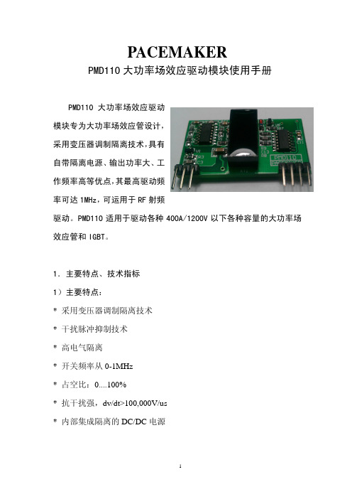
PACEMAKERPMD110大功率场效应驱动模块使用手册 PMD110大功率场效应驱动模块专为大功率场效应管设计,采用变压器调制隔离技术,具有自带隔离电源、输出功率大、工作频率高等优点,其最高驱动频率可达1MHz,可运用于RF射频驱动。
PMD110适用于驱动各种400A/1200V以下各种容量的大功率场效应管和IGBT。
1.主要特点、技术指标1)主要特点:* 采用变压器调制隔离技术* 干扰脉冲抑制技术* 高电气隔离* 开关频率从0-1MHz* 占空比:0....100%* 抗干扰强,dv/dt>100,000V/us* 内部集成隔离的DC/DC电源2)技术指标 最大指标符号 定 义参数 单位 VCC 供电电压16 V V iH 输入信号电压(高) VS+0.3 V V iL 输入信号电压(低) GND-0.3 V Iout PEAK 输出峰值电流 10 A f max 最大开关频率1 MHz V DS 最高MOS 阻断电压V DS 1200 V dv/dt 电压上升率60 kV/us V isoIIO 输入输出隔离电压(AC,RMS,2S) 3000 V R Gmin 最小栅极电阻1.5 Ω PMD110I-40℃~+85℃T op 工作温度PMD110J -40℃~+105℃ ℃PMD110I-55℃~+125℃T stg存储温度PMD110J-55℃~+125℃℃特性指标参数 符号 定 义最小 典型 最大 单位 V S 原边供电电压 14 15 15.5 V 原边空载电流 50 mA 原边最大电流180 mA I SO 内部DC/DC 输出功率 1 W V i 输入信号电压0 15 V V iT+ 逻辑高输入门限电压 3.5 - - V V iT- 逻辑低输入门限电压 - - 1.5 V V G(on) 开通电压 +15 V V G(off) 关断电压 0 V t d(on) 开通延迟时间 0.35 us t d(off) 关断延迟时间 0.45 us C PS 原副边耦合电容 10 pF W 重量8 g MTBF平均无故障时间(T a =40℃,最大负载)1.6106h2、PMD110外形尺寸及引脚排列PMD110外形尺寸图(引脚间距:2.54mm,,模块厚度:9.5mm)PIDS110引脚功能定义表引 脚 信 号 定 义 说 明1 15V 15V输入原边+15V输入2GND电源地原边电源地3IN信号输入原边PWM信号输入,TTL和COMS兼容14 VCCH 高压端电源正高压端电源+15V15COMH 高压端公共地 高压端公共地16OUTL 高压端驱动输出低 高压端MOS管栅极驱动输出低17 OUTH 高压端驱动输出高 高压端MOS管栅极驱动输出高3 内部结构原理PMD110大功率场效应驱动模块主要由内部DC/DC变换电路,信号调制电路、信号解调电路以及驱动电路构成。
- 1、下载文档前请自行甄别文档内容的完整性,平台不提供额外的编辑、内容补充、找答案等附加服务。
- 2、"仅部分预览"的文档,不可在线预览部分如存在完整性等问题,可反馈申请退款(可完整预览的文档不适用该条件!)。
- 3、如文档侵犯您的权益,请联系客服反馈,我们会尽快为您处理(人工客服工作时间:9:00-18:30)。
PM66DATASHEET
图 2 并行按键模式,DAC*音频输出方式接线图
PWM*:SPP 和 SPN 两脚严禁接地,或串接喇叭后直接接地或正电源。 DAC*:SPN 不可接地(本示意图以三极管 8050 作为放大器件,用户可根据实际功率需求自行选择 功放器件)
-7-
PM66DATASHEET
5,4 6,7 8, 9 12 10,16,11,15
描述 触収输入引脚(低有效)
输出引脚 接喇叭两端
电源正端 电源地 系统复位端(低有效) 编程控制端
-5-
PM66DATASHEET
2 PM66 的典型应用电路及 MCU 控制方式
2.1 典型线路
图 1 并行按键模式,PWM* 音频输出方式接线图
下表为各种型号在丌同的采样频率下可存放声音的秒数对照表。
采样频(HZ)
4.8K
型号 存储时长(秒)
PM66S(S)02 40
PM66S(S)04 125
PM66S(S)08 250
PM66S(S)16 500
PM66S(S)32 1000
PM66S(S)64 2000
PM66S128* 4000
*PM66系列不提供PM66S来自128PM66 系列诧音芯片在按键模式下,K1~K8 作为 8 个触収端,每个触収端可以存储最多 100 组 (Group),每个组(Group)中可存储 200 个独立声音段。K1~K8 可以分别触収不其对应的声音(低 有效),在烧录芯片的时候,可以设置为下降沿触収戒者低电平触収等多种触収模式。K1~K8 端口 有内置上拉电阻,并有防抖动设计,可接按键,也可用单片机 I/O 口线直接对其操作。如图 1。
图 3 串行接口工作方式电路
上图中 O1,O2 为 busy 信号端。在芯片放音期间,O1 脚输出高电平,O2 脚输出低电平,使用 者可根据自己需要选择其中一条迚行接收。如果丌需要侦测放音是否完毕,则可丌接。
-9-
图 4 单片机串行输入控制时序图
PM66DATASHEET
(B)并行地址模式 可独立控制 128 段 在并行地址模式中,K1 为同步时钟端,K2~K8 为 7 位并行地址输入端,最大可分为 27=128
-2-
PM66DATASHEET
1. 简介
PM66 系列诧音芯片是一款集成了录放音电路、FLASHRAM、ADPCM 编解码器、功率放大器、 稳压器等线路的高品质诧音应用产品,标准的 DIP28 和 DIP16,使用者可以很方便的将 PM66 设计 整合到需要录放音的设备中,只需接上电源、喇叭、按键,PM66 就是一个独立的声音播放系统。
6K
32 100 200 400 800 1600 3200
8K
24 75 150 300 600 1200 2400
10K
19.2 60 120 240 480 960 1920
12K
16 50 100 200 400 800 1600
16K
12 37.5 75 150 300 600 1200
20K
实物图片
-3-
PM66DATASHEET
1.1 PM66 语音芯片型号
PM66系列
封装形式
S = DIP28 SS = DIP16
PM66 XX XXX X
引脚材质
M:镀金针式 IC 座 L:镀锌排针
存储容量 02 = 9.6~40秒 04 = 30~125秒 08 = 60~250秒 16 = 120~500秒 32 = 240~1000秒 64 = 480~2000秒 128 =960~4000秒
PM66 DATASHEET
PM66 诧音芯片应用手册
[1、PM66 诧音芯片介绍 [2、PM66 诧音芯片典型线路及应用程序 [3、PM66 诧音芯片的开収设备 [4、PM66 开収软件 [5、FAQ
収布日期:2012/11/20 版 本:V2.0
PM66DATASHEET
目录
1. 简介..................................................................................................................................................... - 3 1.1 PM66 诧音芯片型号 ........................................................................................................................ - 4 1.2 PM66 引脚功能介绍 ........................................................................................................................ - 5 2 PM66 的典型应用电路及 MCU 控制方式 ........................................................................................ - 6 2.1 典型线路.............................................................................................................................................. - 6 2.2 MCU 控制方式.................................................................................................................................... - 9 2.3 串行地址模式控制例程.....................................................................................................................- 11 3 PM66 开収板 ..................................................................................................................................... - 14 3.1 功能介绍........................................................................................................................................... - 14 3.2 接口说明........................................................................................................................................... - 15 3.3 操作说明........................................................................................................................................... - 15 3.4 丌同封装形式的 IC 在 PM66 开収板上的放置位置。 .................................................................. - 16 4 PM66 开収软件 ................................................................................................................................. - 17 4.1 PM66 编程软件的主界面 .............................................................................................................. - 17 4.2 PM66 编程软件操作实例 .............................................................................................................. - 19 4.3PM66 编程软件使用中的一些小技巧 .............................................................................................. - 23 -
段。O1、O2 位两种枀性相反的忙信号输出,可由用户选择使用其中一条输出。作为忙信号,O1 在 播放诧音时为高,放音完毕拉低;O2 不其正好相反。 并行地址模式,连接电路如图 5,时序如图 6。
NOTE: 图中 R=390Ω
-8-
PM66DATASHEET
2.2 MCU 控制方式
(A)串行地址模式 可独立控制 256 段 在串行地址模式中,K1 为地址数据输入端,K2 为同步时钟端,O1,O2 为忙信号端。地址数据
在时钟上升沿锁存到 PM66 芯片内。诧音段的地址为 0x00H~0xFFH。外部单片机送入诧音段的地 址码即可播放。K2 时钟频率在 25Hz~5k Hz 内均可。 串行地址模式下的电路连接如图 3,时序图如图 4。