BT1213H 蓝牙模块规格书V1.0
SJR-BTM625蓝牙模块规格书
Bluetooth Module DatasheetModel:SJR-BTM625Version:V1.02015-11-26Sky Jiarun Technologies Co.,Ltd.Tel:(86755)85279490E-mail:sales@Fuyong,Baoan,ShenzhenList of Contents1Introduction (3)2Key Features (3)3Applications (4)4Block Diagram (4)5General specifications (4)6Module Package Information (5)6.1Pinout Diagram and package dimensions (5)6.2Module Pin descriptions (6)7Electrical Characteristics (8)7.1Absolute Maximum Ratings (8)7.2Recommended Operating Conditions (8)8Recommended reflow temperature profile (9)1IntroductionSky Jiarun Technologies introduces the pioneer of the Bluetooth4.2modules SJR-BTM625which is a high performance,cost effective,low powerand compact solution.The Bluetooth module provides a complete2.4GHzBluetooth system based on the BlueCore CSRA64215chipset which is a singlechip radio and baseband IC for Bluetooth2.4GHz systems,.This module is fullycompliant to Bluetooth v4.2for audio communications.2Key FeaturesBluetooth Profiles●Bluetooth v4.2specification support●A2DP v1.3●AVRCP v1.6●HFP v1.6●HSP v1.2●DI v1.3Music Enhancements●aptX,aptX Low Latency,SBC and AAC●TrueWireless Stereo(TWS)●Configurable Signal Detection to trigger events●Up to10stages of Speaker Parametric EQ●Up to6banks of5stages of User Parametric EQ for music playback(user,rock,pop,classical,jazz,etc)●MeloD Expansion3D stereo widening and phase shifting effect●Volume Control●Compander to compress or expand the dynamic range of the audio●Post Mastering to improve DAC fidelity●Volume BoostAdditional Functionality●Support for multi-language programmable audio prompts●CSR's proximity pairing and CSR's proximity connection●Multipoint support for A2DP connection to2A2DP sources for music playback●Talk-time extension●Slim module with28.5mm x13mm x2.0mm3Applications●Stereo Headsets●Wired Stereo headsets and headphones●Portable Bluetooth Stereo speakers4Block Diagram5General specificationsModel Name SJR-BTM625Product Description Bluetooth4.2Class2Module Bluetooth Standard Bluetooth4.2Chipset CSRA64215Dimension28.5mm x13mm x2.0mmOperating ConditionsVoltage 2.8~4.2VTemperature-10~+70℃Storage Temperature-40~+85℃Electrical SpecificationsFrequency Range2402~2480MHzMaximum RF Transmit Power4dBmπ/4DQPSK Receive Sensitivity-82dBm8DPSK Receive Sensitivity-92dBm6Module Package Information6.1Pinout Diagram and package dimensionsUnit:MMRecommended PCB layout footprint6.2Module PindescriptionsPinNo.Pin Name Pin Type Description1PIO6Bidirectional with strong pull-down Programmable input/output line62PIO8Bidirectional with strong pull-up Programmable input/output line83PIO1Bidirectional with strong pull-up Programmable input/output line14PIO0Bidirectional with strong pull-up Programmable input/output line05LED1Bidirectional LED driver6AIO0Bidirectional Analogue programmable input/output line 7PIO17Bidirectional with strong pull-down Programmable input/output line178PIO9Bidirectional with strong pull-down Programmable input/output line99PIO7Bidirectional with strong pull-down Programmable input/output line7101V8 1.8V output 1.8V output for keys11PIO16Bidirectional with strong pull-up Programmable input/output line1612CHG_EXT Charger external pin External battery charger control. External battery charger transistor base control when using external charger boost.Otherwise leave unconnected.13VBAT_SENSE Battery Sense Battery charger sense input14PIO21Bidirectional with weak pull-down Programmable input/output line21 15PIO18Bidirectional with weak pull-down Programmable input/output line1816SPI_PCM#Input with weak pull-down SPI/PCM select input: 0=PCM/PIO interface 1=SPI17GND VSS Ground18USB_P Bidirectional USB data plus 19USB_N Bidirectional USB data minus20RSTn Input with strong pull-up Reset if low.Pull low for minimum 5ms to cause a reset.21SPI_MOSI Bidirectional with weak pull-down Programmable input/output line2 Alternative function:SPI_MOSI:Debug SPI data input PCM1_IN:PCM1synchronous data inputI2S1_SD_IN:I²S1synchronous data inputSPDIF_IN:SPDIF input22SPI_CLK Bidirectional with weak pull-down Programmable input/output line5 Alternative function:SPI_CLK:Debug SPI clockPCM1_CLK:PCM1synchronous data clockI2S1_SCK:I²S1synchronous data clock23SPI_CSB Bidirectional with weak pull-down Programmable input/output line4 Alternative function:SPI_CS#:chip select for Debug SPI,active lowPCM1_SYNC:PCM1synchronous data syncI2S1_WS:I²S1word select24SPI_MISO Bidirectional with weak pull-down Programmable input/output line3 Alternative function:SPI_MISO:Debug SPI data output PCM1_OUT:PCM1synchronous data outputI2S1_SD_OUT:I²S1synchronous data output25VCHG Charger voltage input Internal charger input for charging26GND VSS Ground27VBAT Battery positive terminal Power supply input for2.7~4.2V28LED0Bidirectional LED driver29LED2Bidirectional LED driver30VREG_EN Power on/off key input Power on/off input key indication31MIC BIAS Analog Microphone bias output32LINE_BN Analog input Line input negative,channel B33LINE_BP Analog input Line input positive,channel B34LINE/MIC_AP Analog input Line or microphone input positive,channel A 35LINE/MIC_AN Analog input Line or microphone input negative,channel A 36SPK_BN Analog output Speaker output negative right37SPK_BP Analog output Speaker output positive right38SPK_AN Analog output Speaker output negative left39SPK_AP Analog output Speaker output positive left40GND VSS Ground7Electrical Characteristics7.1Absolute Maximum RatingsRating Minimum MaximumStorage temperature-40℃+85℃7.2Recommended Operating ConditionsOperating Condition Minimum MaximumOperating temperature range-10℃+70℃Supply voltage:VBAT+2.8V+4.2V8Recommended reflow temperature profileThe module Must go through125℃baking for at least9hours before SMTAND IR reflow process!若拆封后未立即上线,天嘉润科技建议让下次上线前务必以125℃烘烤9小时以上!Record of ChangesData Revision Description2015-11-26V1.0Original publication of this document.IMPORTANT NOTICESky Jiarun Technologies Co.,Ltd(SJR)reserve the right to make changes to their products or to discontinue any product or service without notice,and advisecustomers to obtain the latest version of relevant information to verify,beforeplacing orders,that information being relied on is current.All products are sold subject to the SJR terms and conditions of sale supplied at the time of orderacknowledgement,including those pertaining to warranty,patent infringement, and limitation of liability.SJR warrants performance of its products to specifications applicable at the time of sale in accordance with SJR’s standard warranty.Testing and other qualitycontrol techniques are utilized to the extent SJR deems necessary to support this warranty.Specific testing of all parameters of each device is not necessarilyperformed,except those mandated by government requirements.In order to minimize risks associated with customer applications,adequatedesign and operating safeguards must be used by the customer to minimizeinherent or procedural hazards.SJR products are not authorized for use as critical components in life support devices or systems without the express writtenapproval of an officer of the company.Life support devices or systems aredevices or systems that are intended for surgical implant into the body,orsupport or sustain life,and whose failure to perform when properly used inaccordance with instructions for use provided,can be reasonably expected toresult in a significant injury to the user.A critical component is any component ofa life support device or system whose failure to perform can be reasonablyexpected to cause the failure of the life support device or system,or to affect its safety or effectiveness.SJR assumes no liability for applications assistance or customer product design.SJR does not warrant or represent that any license,either express or implied,is granted under any patent right,mask work right,or other intellectual propertyright of SJR covering or relating or any combination,machine,or process in which such products or services might be or are used.Tel:(86755)85279490Fax:(86755)85279683E-mail:sales@。
蓝牙-BT规格书

蓝牙-BT规格书HSP: headset耳机功能,提供移动终端与耳机之间通信所需的基本功能,如:配对连接,接听来电,挂断电话。
HFP: handsfree供免提设备拨打和接听呼叫, 是HSP的扩展,常用于车载免提,让蓝牙设备可以控制电话,如接听、挂断、拒接、语音拨号等,A2DP(立体声)蓝牙音频传输模型协定, 是专门为使用蓝牙传送立体声音乐而制定的:A2DP能够让两个同样支持蓝牙音效传输的装置互相连接能输出如CD音质(16 bits,44.1 kHz)般的音乐, 假如有一方没有支持A2DP的话,这时音效就只能输出HandsfreeProfile(8 bits,8kHz),就算耳机是采用双耳筒的设计,也只能有一般电话的单声道音质,与真正的立体声相去甚远。
验证方法:蓝牙立体声耳机推出进行Skype通话,听音乐,通话等,终端有Media Player或类似的音乐播放器功能AVRCP(音乐播放控制)音频/视频远程控制配置文件,设计用于提供控制TV、Hi-Fi设备等的标准接口。
此配置文件用于许可单个远程控制设备(或其它设备)控制所有用户可以接入的A/V设备。
它可以与A2DP或VDP配合使用,VRCP 定义了如何控制流媒体的特征。
包括暂停、停止、启动重放、音量控制及其它类型的远程控制操作。
SPP串行端口配置,定义了如何设置虚拟串行端口及如何连接两个蓝牙设备将两台设备作为虚拟串行端口,然后通过蓝牙技术连接两台设备定义了两个角色,设备 A 和设备 B。
设备 A——即主动建立至另一设备的连接的设备(发起方)。
设备 B——即等待另一设备主动建立连接的设备(接收方)BIP为基本图像规范,典型的应用如使用手机控制数码相机的快门操作,在设备之间传送图像,可分为:1、Image Push 该应用允许蓝牙主单元向从单元发送一幅或多幅图像,进而从单元可将接受到的图像显示或打印出来。
2、Image Pull允许蓝牙主单元查阅存储于从单元的图像,并在从单元用户允许的情况下,下载查阅的图像。
BT8123 规格书

BT8123规格书文件编号:VS_11061501版本:V1.0日期: 2013-7-12深圳市百泰实业有限公司地址: 深圳宝安区西乡镇固戍村榆盛工业区6栋6楼东TEL: +86-755-27491316/26/36FAX: +86-755-27491346BT8123—恒定5.0W输出功率、FM无干扰F类音频功率放大器一 概述BT8123是一款F类音频功率放大器。
内置的BOOST功率模块在4Ω负载时,5W和3.7W两个功率点之间可选。
当BOOST模块在3.7W的情况下,4Ω的负载时功率恒定,并通过MUCH使能端的控制,BOOST模块可以单独提供最高可达2A的电流输出;当BOOST模块在5W的情况下,4Ω的负载时功率恒定.AB类D类可切换模式的设计,最大限度的减少音频子系统中功放对FM的干扰. BT8123在锂电池的供电电压范围内提供了极致的功率输出,使得BT8123成为便携式音箱设备特别是扩音器产品的最优选择. BT8123的全差分架构和极高的PSRR有效地提高了BT8123对RF噪声的抑制能力。
无需滤波器的PWM调制结构及内置的BOOST功率选择模块,尽可能的减少了外围器件,另外BT8123内置了过流保护,短路保护和过热保护,有效的保护芯片在异常的工作条件下不被损坏。
BT8123提供了纤小的的SOP16L封装形式供客户选择,其额定的工作温度范围为-40℃至85℃二 特点● 内置BOOST模块,AB类D类集成的特殊F类结构● 输出功率PO at 10% THD+N, VIN = 3.7VRL = 4Ω 3.70W(BOOST 功率值为3.7W)RL = 4Ω 5.00W(BOOST 功率值为5W )● 优异的"噼噗-咔嗒"(pop-noise)杂音抑制能力● 工作电压范围:2.5V到5.0V● MUCH功能:功放静音同时,PVDD可输出最高2A的电流● 无需滤波的Class-D结构● 72%的效率● 高电源抑制比(PSRR):在217Hz下为70dB● 启动时间 (260ms)● 静态电流 (10mA)● 低关断电流 (<0.1µA)● 过流保护,短路保护和过热保护● 符合Rohs标准的无铅封装三 管脚排列图四极限参数五推荐工作参数六电气参数七工作特性八应用线路图九典型特征曲线(TA=25°C, RL = 4Ω,ΑΒD=1,VMODE=1(D类模式除非特殊说明)类模式 除非特殊说明)(TA=25°C, RL=4Ω,ABD=0(AB去耦电容(Cs)BT8123是一款高性能音频放大器,电源端需要加适当的电源供电去耦电容来确保其高效率和最佳的总谐波失真。
gh300 数据手册说明书
3 电源管理和复位 ..................................................................................................................................................... 6 3.1 芯片上电时序................................................................................................................................................. 6 3.2 复位................................................................................................................................................................. 6
BT1213H 蓝牙模块规格书V1.0

BOOMTECH SEMICONDUCTORS CO.,LTDProduct SpecificationModel : BT1213HREV : V1.0DRAWN BY :CHECKED BY :APPD BY:1. IntroductionBoomtech Semiconductors Co., Ltd the pioneer of the Bluetooth 4.0 modulesBT1213H which is a high performance, cost effective, low power and compact solution. The Bluetooth module provides a complete 2.4GHz Bluetooth systembased on CSR 8635 chip which is a single-chip radio and baseband IC for Bluetooth 2.4GHz systems including basic rate, EDR to 3Mbps and Bluetooth low energy2. Key Features• Fully Qualified Single-chip Bluetooth® v4.0 System•-91dBm (typical) π/4 DQPSK receiver sensitivityand -81dBm (typical) 8DPSK receiver sensitivity• A2DP v1.2, multipoint A2DP support enables connection to 2 A2DPsource devices for music playback• CSR's latest CVC technology for narrowband andwideband voice connections including wind noise reduction• AVRCP v1.4• Wideband speech supported by HFP v1.6 and mSBC codec•Audio interfaces: I²S and PCM• Stereo codec with 1 microphone input• 5-band fully configurable EQ• SBC, MP3 and AAC decoder support• Wired audio supportSupported sample rates of 8, 11.025, 16, 22.05, 32,44.1, 48 and 96kHz (DAC only)■Bluetooth low energy• Dual-mode Bluetooth low energy radio• Support for Bluetooth basic rate / EDR and low energy connections• 3 Bluetooth low energy connections at the same time as basic rate A2DP• Slim module with 24.5mm x 14.1mm x 2.0mm• RoHS Compliant3. Applications• Stereo speakers• Speakerphones• Handsfree car kits• 1-mic stereo headset or headphones6. Module Package Information6.1 Pinout Diagram and package dimensions 6.2 Module Pin descriptionsPIN NO.Pin Name1GND 2UART_TX 3UART_RX 4UART_RTS 5UART_CTS 6PIO 7PIO 8PIO 9PIO 10SPI_EN 11PCM1_IN UART data output for debug only / PIO15 Ground Description UART data input for debug only / PIO14 UART request to send, active low / PIO16 UART clear to send,active low / PIO17 PCM1 synchronous data input/SPI_MOSIfor debug only for debug only SPI/PCM select input for debug only for debug only12PCM1_CLK 13PCM1_OUT 14PCM1_SYNC15RESET16LED2(BLUE) 17LED1(RED) 18MFB/POWER 19CHARGE20VBAT211V822GND23USB_N24USB_P25PIO726PIO/027PIO628PIO1829PIO2130LED331LINE/MIC_AN32LINE/MIC_AP 33MIC_BIAS34LINE_BN35LINE_BP36SPK_RN37SPK_RP38SPK_LN39SPK_LP40GND LINE/MIC_AP input positiveLINE_BN input negativeLINE_BP input positiveMicrophone biasProgrammable input / output line 7PCM1 synchronous data sync/SPI_CSPCM1 synchronous data clock/SPI_CLKPCM1 synchronous data output/SPI_MISOLED driver(Open drain output)LED driver(Open drain output)Programmable input / output line 21LINE/MIC_AN input negativeProgrammable input / output line 18LED driver(Open drain output)Internal 1.8VPower on/off input key indicationReset if low. Input debounced so must be low for >5ms to cause a resetInternal charger input for charging(5V)Battery Power supply input for 3.0~4.2VUSB data minusUSB data plus with selectable internal1.5kΩ pull-up resistorProgrammable input / output line 6GroundProgrammable input / output line 0Speaker output negative,rightGroundSpeaker output positive,rightSpeaker output negative,leftSpeaker output positive,left7. Example Application Schematic。
ASUS USB-BT211 bluetooth receiver Manual说明书
包裝內容物
請檢查以下配件是否齊全:
華碩 USB-BT211 驅動程式與應用程式光碟(使用手冊、應用程式) 快速使用指南
第 1 章:認識您的 USB 藍牙接收器 藍牙(Bluetooth®)概觀......................................................................................1 包裝內容物................................................................................................................1 系統需求.....................................................................................................................1 USB-BT211 規格概要............................................................................................2
Windows® XP / Vista / 7 傳送典型值:51mA,接收典型值:43mA,待機 模式:15mA DC 5V,透過 USB 連接埠供電 <-85dBm 於 <0.1% BER 19.52 x 13.5 x 6.8 mm (L x W x H) 2.2g 0℃ ~ 60℃ (32℉ ~ 140℉) -10℃ ~ 70℃ (14℉ ~ 158℉) 5% ~ 90%,非凝結
SJR-BTM870-C蓝牙模块规格书

Units dBm dBm dB dB dB dB dB
Min -20 Min 0 16 -
Typ -90 -10 6 -6 -38 -45 -16 Typ 3 24 0.5 940 -36 -45
Max -86 11 0 -30 -40 -9 Max 1000 -20 -40
Spec-BTM870-C-V1.0
Page 2 of 6
Product Specification
9 10 11 12 13 14 15 16 17 18 19 20 21 22 23 24 25 26 27 28 29 30 31 SPI_CLK SPI_MISO SPI_CSB SPI_MOSI UART_RX UART_TX LED0 LED1 LED2 RESET PIO10 PIO11 PIO12 PIO13 I2C_SCL I2C_SDA GND USB_D+ USB_DGND V5.0 1V8_OUT VDD_PADS CMOS Input CMOS Output CMOS Input CMOS Input CMOS Input CMOS Output Open drain output Open drain output Open drain output CMOS input with weak internal pull-up Bi-directional Bi-directional Bi-directional Bi-directional Bi-directional Bi-directional GND Bi-directional Bi-directional GND Power Power Power Serial Peripheral Interface Clock Serial Peripheral Interface Data Output Chip Select For Synchronous Serial Interface (Active Low) Serial Peripheral Interface Data Input UART Data Input (Active High) UART Data Output (Active High) LED Driver LED Driver LED Driver Reset if low. Input debounced so must be low for >5ms to cause a reset Programmable Input/Output Line Programmable Input/Output Line Programmable Input/Output Line Programmable Input/Output Line Programmable Input/Output Line(Serial Clock) Programmable Input/Output Line(Serial Address/Data I/O) Ground USB Data Plus USB Data Minus Ground Battery charger input 1.8V switch-mode power regulator output 1.7V to 3.6V positive supply input for input/output ports: ■RST# ■UART ■PCM ■ SPI ■ PIO[15:0] 1.7V to 3.6V positive supply input for input/output ports: ■ Serial quad I/O flash port Take high to enable switch-mode regulator Battery positive terminal Ground Programmable Input/Output Line, SPI flash clock Programmable Input/Output Line, SPI RAM click Programmable Input/Output Line, SPI flash chip select Programmable Input/Output Line, SPI RMA chip select Programmable Input/Output Line, Serial quad I/O flash data bit 0 Programmable Input/Output Line, Serial quad I/O flash data bit 1 Programmable Input/Output Line, Serial quad I/O flash data bit 2 Programmable Input/Output Line, Serial quad I/O flash data bit 3 Ground Microphone bias A Microphone bias B Microphone input negative, right Microphone input positive, right Microphone input negative, left Microphone input positive, left Ground Speaker output negative, left Speaker output positive, left Speaker output negative, right Speaker output positive, right Ground Bluetooth 50Ω transmitter output /receiver input Ground
蓝牙模块[BT11_Datasheet]
![蓝牙模块[BT11_Datasheet]](https://img.taocdn.com/s3/m/84a55a114431b90d6c85c7c5.png)
Contents
1 1.2 1.3 1.4 1.5 2 2.1 2.1.1 2.1.2 2.1.3 2.1.4 2.1.5 2.2 2.2.1 2.2.2 2.2.3 2.2.4 2.2.5 2.3 2.4 3 4 4.1 4.2 4.3 4.4 4.5 4.5.1 4.5.2 5 5.1 6 7 8 Software Architecture........................................................................................................................................ 3 Lower Layer Stack............................................................................................................................................3 Upper Layer Stack: Amp’ed UP..................................................................................................................... 3 HCI Interface.........................................................
BT1200蓝牙模块规格书1.1
深圳市百泰实业有限公司Product SpecificationModel : BT1200REV : 1.1DRAWN BY :CHECKED BY :APPD. BY:一、功能特性• 支持V2.0+EDR版蓝牙规范• 输出功率类别为Class 2(Bluetooth radio with +2dBm transmit power and-83dBM receive sensitivity)• 支持A2DP立体声播放(supports A2DP V1.2 and AVRCP V• 模块专为蓝牙音箱类产品应用而设计• 规格尺寸:21mm x 21mm x 2.0mm1.1 radio• Bluetooth V2.0 + EDR specification compliant system in 2.4GHz ISM band• typical +2 dbm transmit power• typical -83 dBm receive sensitivity• on-chip Bluetooth stack allows full-speed data transfer and Piconet support• on-chip A2DP V1.2 and AVRCP V1.4 profiles with hardware SBC decoder enables audiostream over Bluetooth and remote control1.2. baseband processor• on-chip low power, high performance, 32-bit RISC processor• 2Mb internal ROM and 48kB internal RAM• integrated one-time programmable (OTP) ROM for device configuration data• fully integrated Bluetooth baseband logic for FEC, HEC, access code correlation, CRC, demodulation, encryption bit stream generation, whitening• fully supports Bluetooth V2.0 + EDR features including AFH and enhanced datarate up to 3Mbps• supports CVSD transcoder for voice over air1.3 stereo audio CODEC• integrated high fidelity audio CODEC with SNR > 90dB playback• on-chip 20-bit stereo audio digital-to-analog converter (DAC)• on-chip 16-bit mono voice analog-to-digital converter (ADC)• integrated headphone amplifier in 40mW @ 32Ω supporting capacitor-less output• one-channel microphone input with microphone driver二、规格说明2.1 transmitter characteristics2.2 receiver characteristics2.5 digital to analog converter characteristicsa2.6 POWER CONSUMPTION 功耗测试NOMINALLIMIT55≦702.7 COMMUNICATION RANGE 通信距离NOMINALLIMIT8+/-1/8-122.8电性参数4.2VMin-40°C Max +100°C90% Min -10°C 3.3VMax +80°C mAUNIT正常通信距离(直线无障碍物)M 最大通信距离(直线无障碍物)MUNITplay MODE CURRENT 音乐电流(最大音量档)存储条件DESCRIPTIONDESCRIPTION存储温度 相对湿度建议工作条件 工作温度范围 工作电压(VCC)0%三、功能方块图表四、PIN脚功能说明PIN脚编号123、222145678PLAY/PAUSE 播放/暂停按键信号9NEXT 下一曲10PREVIOUS 上一曲11VOL+12UART接收信号13VBUCK 内部电源输出脚1415、19、23161817、20空脚BAT_IN 电池电源输入端(3.3-4.2V)注意:电源电压不可超过4.3V GND接地端MIC MIC输入R声道音频输出LED驱动输出(blue)功能说明开关机按键信号L声道音频输出音频输出公共端LED驱动输出(red)ONKEYAudio_COM Audio_R-LED-RED RESET UART_RX UART_TXNCLED-BLUE Audio_L 名称复位控制输入(低电平有效)音量减按键信号/复用上一曲UART发送信号VOL-音量加按键信号/复用下一曲。
ESP-12H规格书说明书

ESP-12H规格书版本V1.0版权©2020免责申明和版权公告本文中的信息,包括供参考的URL地址,如有变更,恕不另行通知。
文档“按现状”提供,不负任何担保责任,包括对适销性、适用于特定用途或非侵权性的任何担保,和任何提案、规格或样品在他处提到的任何担保。
本文档不负任何责任,包括使用本文档内信息产生的侵犯任何专利权行为的责任。
本文档在此未以禁止反言或其他方式授予任何知识产权使用许可,不管是明示许可还是暗示许可。
文中所得测试数据均为安信可实验室测试所得,实际结果可能略有差异。
Wi-Fi联盟成员标志归Wi-Fi联盟所有。
文中提到的所有商标名称、商标和注册商标均属其各自所有者的财产,特此声明。
最终解释权归深圳市安信可科技有限公司所有。
注意由于产品版本升级或其他原因,本手册内容有可能变更。
深圳市安信可科技有限公司保留在没有任何通知或者提示的情况下对本手册的内容进行修改的权利。
本手册仅作为使用指导,深圳市安信可科技有限公司尽全力在本手册中提供准确的信息,但是深圳市安信可科技有限公司并不确保手册内容完全没有错误,本手册中的所有陈述、信息和建议也不构成任何明示或暗示的担保。
文件制定/修订/废止履历表版本日期制定/修订内容制定核准V1.02020.09.23首次制定邓朝美徐宏目录一、产品概述 (5)二、电气参数 (8)三、外观尺寸 (10)四、管脚定义 (12)五、原理图 (14)六、设计指导 (14)七、回流焊曲线图 (17)八、包装信息 (18)九、联系我们 (18)一、产品概述ESP-12H是由深圳市安信可科技有限公司开发的Wi-Fi模块,该模块核心处理器ESP32-S2F是一款高集成度的低功耗Wi-Fi系统级芯片(SoC),专为物联网(IoT)、移动设备、可穿戴电子设备、智能家居等各种应用而设计。
ESP32-S2F具有行业领先的低功耗性能和射频性能,支持IEEE802.11b/g/n协议,集成了Wi-Fi MAC、Wi-Fi射频和基带、射频开关、射频Balun、功率放大器、低噪声放大器等。
PAN1026A蓝牙基本数据率和低功耗模块设计指南(版本1.1)说明书
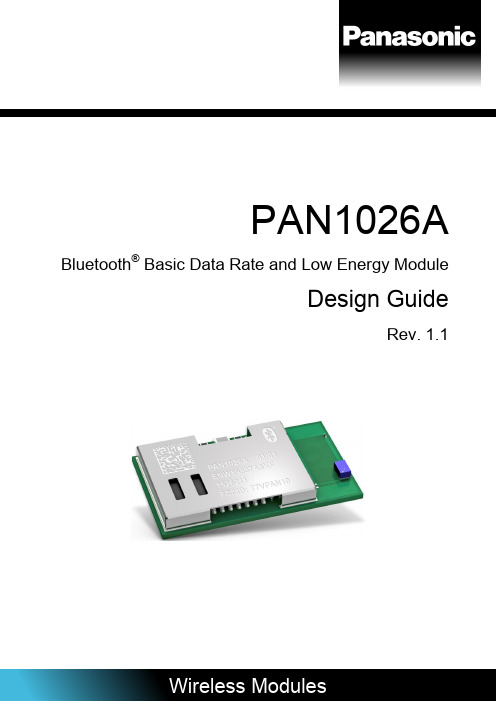
PAN1026ABluetooth ® Basic Data Rate and Low Energy ModuleDesign GuideRev. 1.1OverviewThe PAN1026A is a Class 2 Bluetooth 4.2 Basic Data Rate and Low Energy (LE) module for easy implementation of Bluetooth functionality into various electronic devices.Features•Small SMD module: 15.6 mm x 8.7 mm x 1.8 mm •Same form factor as PAN1760A and PAN1762 •Bluetooth 4.2 Basic Data Rate and LE compliant •Bluetooth stack in ROM•Embedded Basic Data Rate Serial PortProfile (SPP) profile•Embedded LE GATT profile •Supported by Toshiba Bluetooth SDK •UART, 10 General Purpose I/Os, wake up control pinsBluetooth•Basic Data Rate SPP profile•LE Peripheral and Broadcast support•LE GATT server and GATT client support •LE Central and Observer not supported Basic Data Rate Features •Faster SPP classic connection and disconnectiontimes•Support for interlaced inquiry and page scan •Support for extended inquiry responseLow Energy Features •Increased LE MTU size of 160 bytes •Increased number of supported GATT services •Increased number of supported GATTcharacteristics•Support for TX power control•Support for LE Secure Connections •Improved peak error rate (PER) Characteristics•Typical sensitivity: -88 dBm•Output power: max. 4 dBm•Typical TX power consumption: 46 mA •Voltage range: 2.7 V to 3.6 V (+/-10 %)•Temperature range: -40 °C to +85 °CBlock DiagramBy purchase of any of the products described in this document the customer accepts the document's validity and declares their agreement and understanding of its contents and recommendations. Panasonic Industrial Devices Europe GmbH (Panasonic) reserves the right to make changes as required at any time without notification. Please consult the most recently issued Design Guide before initiating or completing a design.© Panasonic Industrial Devices Europe GmbH 2019.This specification sheet is copyrighted. Reproduction of this document is permissible only if reproduction is without alteration and is accompanied by all associated warranties, conditions, limitations, and notices. Do not disclose it to a third party.All rights reserved.This Design Guide does not lodge the claim to be complete and free of mistakes.Engineering Samples (ES)If Engineering Samples are delivered to the customer, these samples have the status “Engineering Samples”. This means that the design of this product is not yet concluded. Engineering Samples may be partially or fully functional, and they may differ from the published Product Specification.Engineering Samples are not qualified and they are not to be used for reliability testing or series production.DisclaimerThe customer acknowledges that samples may deviate from the Design Guide and may bear defects due to their status of development and the lack of qualification mentioned above.Panasonic rejects any liability or product warranty for Engineering Samples. In particular, Panasonic disclaims liability for damages caused by:∙The use of the Engineering Sample other than for evaluation purposes, particularly the installation or integration in another product to be sold by the customer,∙Deviation or lapse in function of the Engineering Sample,∙Improper use of the Engineering Sample.Panasonic Industrial Devices Europe GmbH disclaims any liability for consequential and incidental damages. In case of any queries regarding the Engineering Samples, please contact your local sales partner or the related product manager.Table of Contents1About This Document (5)1.1Purpose and Audience (5)1.2Revision History (5)1.3Use of Symbols (5)1.4Related Documents (6)2Overview (7)2.1Block Diagram (7)2.2Pin Configuration (8)2.3UART Interface (10)2.4Bluetooth Features (10)3Reference Design (11)3.1USB Evaluation Kit Schematic (11)3.2Placement Recommendations (11)4Software Related Documents Summary (13)4.1Predefined High Level APIs (13)4.2Validation of Elliptic Curve Parameters (14)4.3Unique Mac/Bluetooth Address (14)5USB Evaluation Kit (15)5.1Overview for the USB Evaluation Board Options (15)5.2Recommended Tools (16)5.3Development of Applications (16)6Appendix (17)6.1Ordering Information (17)6.2Contact Details (18)1 About This Document1.1 Purpose and AudienceThis Design Guide applies to the Bluetooth development platform PAN1026A USB.The intention is to enable our customers to easily and fast integrate our module PAN1026A in their product.This Design Guide describes the hardware and gives useful hints.It is intended for hardware and software engineers. The product is referred to as“the PAN1026A” or “the module” within this document.1.2 Revision History1.3 Use of SymbolsNoteIndicates important information for the proper use of the product.Non-observance can lead to errors.AttentionIndicates important notes that, if not observed, can put the productat risk.TipIndicates useful information designed to facilitate working with the module.1.4 Related DocumentsPlease refer to the Panasonic website for related documents 6.2.2 Product Information.2 OverviewThe PAN1026A is a Bluetooth 4.2 Basic Data Rate and LE module based on the ToshibaTC35661 single-chip controller.It has both a Bluetooth Basic Data Rate Serial Port Profile (SPP) and a Bluetooth LE GATTprofile stack integrated. Enhanced Data Rate (EDR) and GATT Central Mode are notsupported.Only one connection (either Bluetooth Basic Data Rate or LE) at a time is supported,simultaneous operation of Bluetooth Basic Data Rate and LE is not possible.The integrated EEPROM is pre-programmed with a Bluetooth Device Address and can be used to store additional application information such as connection link keys.Compared to the PAN1026, the PAN1026A is fully backwards compatible, but has additionalsupport for increased MTU size, increased number of services and characteristics and now also supports LE Secure Connections.Previously developed Bluetooth LE profiles and applications can be easily migrated with aminimal effort.Please refer to the Panasonic website for related documents ☯ 6.2.2 Product Information.Further information on the variants and versions☯ 6.1 Ordering Information.2.1 Block Diagram2.2 Pin ConfigurationPin AssignmentTop ViewPin Functions2.3 UART Interface•Full-Duplex 4-wire data transfer: Rx, Tx, RTS, CTS•Programmable baud rate: 2 400 bps to 4.33 Mbps•Default baud rate: 115 200 bps•Data format: 8N1, LSB first•Error detection: Character timeout, Overrun error, Framing error2.4 Bluetooth Features•Bluetooth 4.2 with SPP and GATT•GAP support for SPP•GATT server and client mode supported for LE•Class 2 Tc power with or without external PA (improved link robustness)•Excellent link budget (up to 91 dB), enabling long-range applications•GAP peripheral support for LE3 Reference Design3.1 USB Evaluation Kit Schematic3.2 Placement RecommendationsAntennaDo not place any ground plane under the marked restricted antenna area inany layer! This would be affecting the performance of the chip antenna in acritical manner.The following requirements must be met:✓Keep this product away from heat. Heat is the major cause of decreasing the life of these products.✓Keep this product away from other high frequency circuits.Antenna “Keep o ut Area”The antenna requires a cutout area of 5 mm x 3 mm under the PAN1026A module. This “Keep out Area” shall be located in every layer under the module antenna.Impact of Placement on the Antenna Radiation PatternThe placement of the module, surrounding material, and customercomponents have an impact on the radiation pattern of the antenna.It is recommended to verify the perfect position of the module in the target application before fixing the design.4 Software Related Documents Summary4.1 Predefined High Level APIsMake use of the easy-to-use High-Level SPP and Bluetooth LE API for PAN1026A setup,connect and data transfer in an easy way. Driver layer provide access to the entire function setof the module. SPP and Bluetooth LE application example is available on Toshiba ARM ®Cortex ®-M3 MCU with FreeRTOS integration.High Level SPP APIs are sufficient for communication with a remote SPP device. With the LE+GATT Driver the use of PAN1026A Command Interface is simplified. It encapsulates Chiron LE MNG, GAP and GATT Commands in one.4.2 Validation of Elliptic Curve ParametersResearchers at the Israel Institute of Technology identified a security vulnerability in two related Bluetooth features: Secure Simple Pairing and LE Secure Connections.PAN1026A supports those features but does not perform public key validation during the pairing procedure. In this case, connections between devices could be vulnerable to aman-in-the-middle attack that would allow for the monitoring or manipulation of traffic.To remedy the vulnerability, the Bluetooth SIG has now updated the Bluetooth specification to require products to validate any public key received as part of public key-based securityprocedures. In addition, the Bluetooth SIG has added testing for this vulnerability within theBluetooth Qualification Program.The necessary procedures are included starting with the release of the Toshiba Bluetooth SDK version 4.2.2. Further information is included in the documentationToshiba_Bluetooth_Platform_Errata.pdf contained in the SDK.To ensure that the end product is operating according to the Bluetoothspecification the customer application has to follow the above mentionedinstructions.4.3 Unique Mac/Bluetooth AddressThe PAN1026A has a preprogrammed address in the EEPROM that needs to be copied into the RAM during the initialization. Therefore three TCU commands need to be used. Below is anexample with the individual address 00 13 43 00 00 1A.The bold marked Bluetooth address is original and needs to be byte switchedto write into the RAM of the module to be visible in an Bluetooth inquiry asexample.1. Enter the address: 01 08 FC 0B 00 A0 00 00 00 14 5B FF 02 03 01.→The result is: 04 FF 0A 08 00 A0 00 00 00 14 5B 00 00.2. Read the Bluetooth address from E2PROM:01 08 FC 10 00 A1 00 00 00 14 88 FF 10 06 A0 01 01 06 02 00.→The result is:04 FF 11 08 00 A1 00 00 00 14 88 00 10 0600 13 43 00 00 1A.3. Set the address into RAM: 01 13 10 06 1A 00 00 43 13 00.→The result is: 04 0E 04 04 13 10 00.5 USB Evaluation KitPAN1026A USB (easy to use) is a development platform for PAN1026A Bluetooth LE dual module to implement Bluetooth functionality into various electronic devices.The PAN1026A USB is intended for evaluation purpose and can be used together with EasySPP and EasyBLE Software.The API is a very useful abstracted tool, which is described on the Toshiba website.For further details on additional options and services please refer to OptionsUFL-External Antenna USB DirectUFL-external antenna connector can be used if the cap next to the modules shield is moved (de-soldered, soldered) to the other (free) pin.USB DirectUSB DirectUFL-Ext.32KHz LEAntennaClockEEPROM WPUART Exposure5.2 Recommended ToolsEasySPPThe following requirement must be met:Microsoft .NET framework (version 4) which can be downloaded from the Microsoft websiteEasy SPP is the first step to get familiar with the TCU commands. The issued commands canbe copied and then ported to any microcontroller. HyperTerminal is not recommended to usebecause the commands are in binary format.EasyBLEThis tool has the same intention as the EasySPP and shows some example Bluetooth LEprofiles e. g. heart rate sensor. It can be used together with various of the shelf apps running on iPhone and Android phones supporting Bluetooth 4.0. One example is “Wahoo Utility” which is available in the Apples iTunes App Store.EasyBLE documentation includes an application example how to connect PAN1026A USB stick and an iOS device.5.3 Development of ApplicationsPlease contact your local sales office for customized development of your individual application6.2.1 Contact Us.Please note that the individual Mac address is stored in the EEPROM and hasto be loaded into the RAM after each start-up.The following tools are recommended: IAR, J-Link debugger.The BMSKTOPASM369BT(kc) Starter Kit makes it possible to quickly and easily evaluateToshiba’s B luetooth Dual Mode LSI TC35661-5xx in combination with Toshiba ARM®Cortex®-M3 MCU as host MCU. It is made to execute the Toshiba Bluetooth Driver software and debug user application code via an embedded J-Link debugger interface. The TMPM369FDFG Microcontroller offers embedded Ethernet, CAN, USB host, USB device and RS-232connectivity.Starter Kit Content:•Toshiba TOPAS369Bluetooth Board•Segger J-Link JTAG/SWD Emulator with USB interface•J-Link 19-pin Cortex-M Adapter•USB Cable•Rapid Start-Up Guide6 Appendix6.1 Ordering InformationVariants and Versions1 Abbreviation for Minimum Order Quantity (MOQ). The default MOQ for mass production is 1 500 pieces,fewer only on customer demand. Samples for evaluation can be delivered at any quantity via the distributionchannels.2 Samples are available on customer demand.6.2 Contact Details6.2.1 Contact UsPlease contact your local Panasonic Sales office for details on additional product options and services:For Panasonic Sales assistance in the EU, visithttps:///about-us/contact-usEmail: *********************.comFor Panasonic Sales assistance in North America, visit the Panasonic website“Sales & Support” to find assistance near you athttps:///distributorsPlease visit the Panasonic Wireless Technical Forum to submit a question athttps://6.2.2 Product InformationPlease refer to the Panasonic Wireless Connectivity website for further information on ourproducts and related documents:For complete Panasonic product details in the EU, visithttp://pideu.panasonic.de/products/wireless-modules.htmlFor complete Panasonic product details in North America, visit/rfmodules。
BT122 HCI Mode 用户指南说明书

UG513: BT122 HCI Mode User’s GuideThe document contains general assumptions of the HCI mode im-plementation.KEY FEATURES•HCI Mode support•DFU over UART possible in HCI mode•Bluetooth host flexibilityRev. 1.0General Assumptions 1. General Assumptions1.1 Connection to the HostIn the HCI mode, BT122 module acts as a Bluetooth controller (according to the Bluetooth Core nomenclature). HCI mode also requires a connection to a host device, which is achieved using UART interface as the main way of communication and control of the BT122 module.1.2 General RulesBT122 module is based on two main parts:•Texas Instruments CC2564C Bluetooth Dual Mode controller•Silicon Labs microcontrollerAfter restart, the microcontroller initializes the TI radio chip by sending all needed vendor settings and configurations. Next, the micro-controller provides Silicon Labs Bluetooth Stack (the BT Host implementation) and uses that to communicate with the TI controller via the HCI protocol, as described in the Bluetooth Core Specification.In the HCI mode, the microcontroller is also responsible for the TI chip initialization and handling vendor commands. However after that routine, all HCI commands, events, and responses will be passed to and from the main BT122 UART port.1.3 The Initial Proposal for the HCI Mode Firmware PreparationTo create any BT122 project, prepare XML configuration files that are used by BGBuild.exe to generate end firmware. The same con-cept is used to generate the HCI mode firmware, as follows:•Update the UART setting in hardware.xml file, for example:<uart baud="115200" flowcontrol="true"/>•Include a proper library in project.xml file:<software><library in="bt122_HCI"/></software>Additionally, it is possible to turn on a sleep mode.For more details, see UG496: BT122 Project Configuration User’s Guide .HCI Mode Comparison for iWRAP and BT122 2. HCI Mode Comparison for iWRAP and BT122Table 2.1. Comparison of HCI Mode on iWRAP and BT122 | Building a more connected world.Rev. 1.0 | 3Using BT122 Module with Host Bluetooth Stack 3. Using BT122 Module with Host Bluetooth Stack3.1 Custom Module ConfigurationThree API commands are available in HCI mode, as follows:•dumo_cmd_system_reset•dumo_cmd_hardware_set_uart_configuration•dumo_cmd_system_get_infoSee BT122 Dual Mode API Reference for detailed command documentation. To configure the serial port, type expected parameter val-ues into the hardware configuration (see UG496: BT122 Project Configuration User’s Guide) or use dumo_cmd_hard-ware_set_uart_configuration command. To update firmware, reset the module in DFU mode with dumo_cmd_system_reset command. Next, update firmware according to section 4.3 of UG497: BT122 User’s Guide.3.2 BlueZ Stack ExampleBT122 module, flashed with HCI firmware, is ready to work with the host Bluetooth stack, for example BlueZ stack. The following are example configuration steps on the code snippet below.Because of resource limitations, set the maximum ACL packet length up to 350 bytes.The highest stable serial port baud rate (for HCI mode) is 2 Mb/s. Higher serial port baud rate is not recommended for host Bluetooth stacks.$ sudo hciattach /dev/ttyUSB0 any 2000000$ sudo hciconfig hci0 aclmtu 350:3$ sudo hciconfig hci0 upAfter correct configuration, BT122 works as Bluetooth dual-mode device.$ hciconfighci0: Type: Primary Bus: UARTBD Address: C4:64:E3:63:8A:AE ACL MTU: 350:3 SCO MTU: 180:4UP RUNNINGRX bytes:21035348 acl:1089757 sco:0 events:722081 errors:0TX bytes:79735765 acl:1137257 sco:0 commands:96 errors:0References 4. References•Silicon Labs, BT122 Dual Mode API Reference, 2021•Silicon Labs, UG496: BT122 Project Configuration User’s Guide, 2021•Silicon Labs, UG497: BT122 User’s Guide, 2021Version History 5. Version HistoryRevision 1.0October, 2021•Initial release.IoT Portfolio/productsQuality /qualitySupport & Community/communitySilicon Laboratories Inc.400 West Cesar Chavez Austin, TX 78701USADisclaimerSilicon Labs intends to provide customers with the latest, accurate, and in-depth documentation of all peripherals and modules available for system and software imple-menters using or intending to use the Silicon Labs products. Characterization data, available modules and peripherals, memory sizes and memory addresses refer to each specific device, and “Typical” parameters provided can and do vary in different applications. Application examples described herein are for illustrative purposes only. Silicon Labs reserves the right to make changes without further notice to the product information, specifications, and descriptions herein, and does not give warranties as to the accuracy or completeness of the included information. Without prior notification, Silicon Labs may update product firmware during the manufacturing process for security or reliability reasons. Such changes will not alter the specifications or the performance of the product. Silicon Labs shall have no liability for the consequences of use of the infor -mation supplied in this document. This document does not imply or expressly grant any license to design or fabricate any integrated circuits. The products are not designed or authorized to be used within any FDA Class III devices, applications for which FDA premarket approval is required or Life Support Systems without the specific written consent of Silicon Labs. A “Life Support System” is any product or system intended to support or sustain life and/or health, which, if it fails, can be reasonably expected to result in significant personal injury or death. Silicon Labs products are not designed or authorized for military applications. Silicon Labs products shall under no circumstances be used in weapons of mass destruction including (but not limited to) nuclear, biological or chemical weapons, or missiles capable of delivering such weapons. Silicon Labs disclaims all express and implied warranties and shall not be responsible or liable for any injuries or damages related to use of a Silicon Labs product in such unauthorized applications. Note: This content may contain offensive terminology that is now obsolete. Silicon Labs is replacing these terms with inclusive language wherever possible. For more information, visit /about-us/inclusive-lexicon-projectTrademark InformationSilicon Laboratories Inc.®, Silicon Laboratories ®, Silicon Labs ®, SiLabs ® and the Silicon Labs logo ®, Bluegiga ®, Bluegiga Logo ®, EFM ®, EFM32®, EFR, Ember ®, Energy Micro, Energy Micro logo and combinations thereof, “the world’s most energy friendly microcontrollers”, Redpine Signals ®, WiSeConnect , n-Link, ThreadArch ®, EZLink ®, EZRadio ®, EZRadioPRO ®, Gecko ®, Gecko OS, Gecko OS Studio, Precision32®, Simplicity Studio ®, Telegesis, the Telegesis Logo ®, USBXpress ® , Zentri, the Zentri logo and Zentri DMS, Z-Wave ®, and others are trademarks or registered trademarks of Silicon Labs. ARM, CORTEX, Cortex-M3 and THUMB are trademarks or registered trademarks of ARM Holdings. Keil is a registered trademark of ARM Limited. Wi-Fi is a registered trademark of the Wi-Fi Alliance. All other products or brand names mentioned herein are trademarks of their respective holders.。
中鸣 X4-RCU 控制器(蓝牙版) 使用手册说明书
使用手册 V1.0
感谢您使用中鸣公司产品。为了安全正确地使用 X4-RCU 控制器,请您在使用之前,仔细阅读本说明书。 广州中鸣数码科技有限公司 2019 年 3 月
目
录
一、X4-RCU 机器人控制器简介.....................................................................................................器人控制器简介
X4-RCU 是广州中鸣数码科技有限公司最新研发的机器人主控器,采用意法半导体公司 新一代 M4 内核的 STM32F407 系列芯片设计而成,接口十分丰富,体积小巧、性能强劲且功 耗极低。该控制器运行速度高达 168MHz,最大处理能力可达 210DMIPS,并且集成 DSP 和 FPU (浮点运算单元),可以轻松应对各种复杂的运算应用场合。全新升级 2.4 英寸高清触摸 屏与 16MB 超大容量存储器,带来良好的操作体验,能完全满足各类竞赛的要求。
三、快速入门...................................................................................................................................... 4
1. 准备物品..................................................................................................................................... 4 2. 安装 ROBOEXP5.X 编程软件......................................................................................................... 5 3. 编程............................................................................................................................................. 5 4. 下载程序..................................................................................................................................... 6 5. 运行程序..................................................................................................................................... 6
BLE Bluetooth module

模块会主动发起断开连接请求 8.1.3、模块处于待机状态时
模块会恢复至出厂预设值状态。 8.2、LED 管脚(PIO1)说明
P0_5
30 PIO7
input/output pin/ADC
P0_4
31 PIO8
input/output pin/ADC
P0_3
32 PIO9
input/output pin/ADC
P0_2
-------------------------------------------------------当前版本 V533 最后修订 2014-11-30 5
置放一个整块的丝印(TopOverLay) 八、系统功能:
本手册只是针对如何使用本公司生产的模块,模块内已经内置应用程序,我 公司不提供任何针对模块做二次开发的支持及技术指导。
模块出厂默认配置: HMSoft: 9600,N,8,1,从模式,iBeacon 关闭, 不休眠, 透传模式 HMSensor:9600,N,8,1,从模式, iBeacon 打开, 自动休眠, 远控模式 如何唤醒休眠中的模块? 有两种方式: 方法一:发送“地瓜地瓜我是土豆,地瓜地瓜我是土豆,地瓜地瓜我是土豆, 地瓜地瓜我是土豆”字符串。 呵呵,开个玩笑,您可以通过发送长度大于等于 80 的字符串来激活模块。 发 送 的 这 个 激 活 字 符 串 不 能 包 含 AT 指 令, 成 功 唤 醒 后 , 串 口 将 会 输 出 “OK+WAKE”字符串。 注: 当 AT+UART 设置为休眠时关闭串口时,您将无法通过此法唤醒模块。 方法二:长按系统按键 1000ms 以上。 关于广播包 从 V528 开始,在 iBeacon 功能关闭的情况下,我们将 MAC 地址加入进了广 播包,方便您能够用统一的 MAC 地址分别在 Android 和 iOS 下识别模块。 Android 下扫描即可得到,iOS 下则放置在厂商数据中,具体请调用 CBAdvertisementDataManufactureDataKey 属性。 数据格式:0x48, 0x4D, 0x00, 0x0E, 0x0B, 0x00, 0x00, 0x00 0x48, 0x4D 为我司”HM”的标识,后面跟的六位即是 MAC 地址。 iOS 下广播包分解后如下图所示:
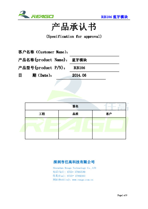
RB106双模蓝牙模块中文规格书V1.2
产品产品承认书承认书承认书(Specification for approval)(Specification for approval)客户名称客户名称((Customer Name Customer Name):): 产品名称(product Name): 蓝牙模块 产品型号(product P/N): RB106 日 期期(Date Date):): 20120120144.0.066签名签名工程工程品质品质客户客户深圳市任高深圳市任高科技科技科技有限公司有限公司有限公司 Shenzhen Reago Technology Co.,LTD电话(Tel): 0755- 27902549 传真(Fax): 0755- 27902263网址(WebSite):1. 产品产品特点特点特点::蓝牙V4.0版本规范 射频功率级别II 级包含传统蓝牙模式和包含传统蓝牙模式和低功耗低功耗低功耗蓝牙模式蓝牙模式采用CSR 最新的CVC 语音增强技术实行语音增强技术实行降噪及回音消除降噪及回音消除 内置16Mb 闪存闪存,,扩展接口可外接最大64Mb SPI 闪存 支持SBC ,MP3,AAC ,APT-X 等多种等多种音频音频音频传输传输传输格式格式 自带6个电容式电容式触摸按键触摸按键 支持iphone 手机手机电量显示电量显示电量显示,,操作语音提示等功能支持A2DP1.2,A VRCP 1.4,HFP1.6(包含支持WBS 和mSBC ),HSP1.2等协议 多种引出接口多种引出接口::PIO/UART/AIO/SPK/MIC/USB/I2S/SPDIF 内置16位立体声编解码器位立体声编解码器,,数模转换信噪比高达95dB 内置直流转换电源管理 集成锂电池充电功能集成锂电池充电功能,,最大充电电流达400mA 极小的BGA 贴片封装贴片封装::14*14*2.8mm PIO 电平可选1.8-3.3V 带屏蔽罩带屏蔽罩,,有效减小干扰RoHS 无铅生产工艺2. 应用领域高品质高品质顶级顶级顶级立体声无线耳机立体声无线耳机 高保真音箱高保真音箱、、音响 电视无线音响系统具有回音消除的无线免提蓝牙汽车影音3. 主要参数工作频段 2.402GHz -2.480GHz ,ISM 频段 蓝牙版本蓝牙版本规范规范 蓝牙V4.0双模 主芯片 CSR8670功率等级 2级 (Class II ) 有效距离有效距离((空旷区域空旷区域)) 10米(典型) 发射功率 +4dBm (典型)接收灵敏度 -88dB at 0.1% BER (典型) 频率偏差 ±10KHz 天线外置电源电压 锂电池电压锂电池电压((3.0-4.3V )尺寸14mm(长) * 14mm(宽) * 2.8mm(高)4. 电气电气参数参数事项最低 典型 最高 单位 存储温度 -30 +20 +85 ℃ 工作工作温度温度 -20 +20 +80 ℃ 供应电压(VBAT) 3.0 3.7 4.3 V 充电输入电压(V_CHG) 4.5 5 5.5 V 内置内置充电器充电电流充电器充电电流 - - 130 mA 外接扩充接扩充充电电流充电电流 - - 400 mA 麦克风输入麦克风输入阻抗阻抗 - 6K - Ω 外接外接麦克风麦克风麦克风灵敏度范围灵敏度范围 -60 - -42 dB 音频输出直流音频输出直流阻抗阻抗16--Ω5. 内部原理框图6. 引脚布局及定义顶层顶层透透视图引脚号引脚号 引脚名称引脚名称 符合电压符合电压脚位描述脚位描述A1A1 SPK_RN SPK_RN 音频差分输出右声道负极音频差分输出右声道负极 A2A2 SPK_SPK_RP RP RP 音频差分输出右声道正极音频差分输出右声道正极 A3A3 GND GND 电源地电源地 A4A4 ANT ANT 射频端口射频端口,,外接天线外接天线 A5A5 GND GND电源地电源地A6A6 MIC_L_BIAS MIC_L_BIAS 1.81.8--2.6V 2.6V左端麦克风供电输出麦克风供电输出 A7A7 MIC_LP MIC_LP 麦克风麦克风差分输入左差分输入左差分输入左端端正极正极 A8A8 MIC_LN MIC_LN 麦克风麦克风差分输入左差分输入左差分输入左端端负极负极 A9A9 FLASH_IO2FLASH_IO2 1.8V 1.8V 外接SPI SPI 闪存写保护端口闪存写保护端口闪存写保护端口 B1B1 CAP5CAP5 1.8V 1.8V 电容式电容式触摸按键触摸按键触摸按键B2B2 SPK_LP SPK_LP 音频差分输出左声道正极音频差分输出左声道正极 B3B3 SPK_LN SPK_LN 音频差分输出左声道负极音频差分输出左声道负极 B4B4 GND GND电源地源地B5B5 MIC_R_BIAS MIC_R_BIAS 1.81.8--2.6V 2.6V右端右端麦克风供电输出麦克风供电输出麦克风供电输出 B6B6 MIC_RN MIC_RN 麦克风麦克风差分输入差分输入差分输入右端右端右端负极负极负极 B7B7 SRAM_CS#SRAM_CS# 1.8V 1.8V 外接SPI RAM 片选端口片选端口 B8B8 SRAM_CLK SRAM_CLK 1.8V 1.8V 外接SPI RAM 时钟端口时钟端口 B9B9 FLASH_IO1FLASH_IO1 1.8V 1.8V 外接SPI SPI 闪存数据输出端口闪存数据输出端口闪存数据输出端口 C1C1 CAP1CAP1 1.8V 1.8V 电容式电容式触摸按键触摸按键触摸按键 C2C2 CAP2CAP2 1.8V 1.8V 电容式电容式触摸按键触摸按键触摸按键 C3C3 CAP0CAP0 1.8V 1.8V 电容式电容式触摸按键触摸按键触摸按键 C4C4 AIO AIO00 <1.35V 1.35V模拟输入模拟输入//输出引脚输出引脚 C5C5 G ND ND 电源地电源地C6C6 MIC_RP MIC_RP 麦克风麦克风差分输入差分输入差分输入右端右端右端正极正极正极 C7C7 FLASH_IO0FLASH_IO0 1.8V 1.8V 外接SPI 闪存数据输入端口闪存数据输入端口 C8C8 FLASH_CS#FLASH_CS# 1.8V 1.8V 外接SPI 闪存片选端口闪存片选端口 C9C9 GND GND 电源地电源地 D1D1 AIO AIO11 <1.35V 1.35V模拟输入模拟输入//输出引脚输出引脚 D2D2 CAP3CAP3 电容式电容式触摸按键触摸按键触摸按键 D3D3 PADS PADS1.81.8--3.33.3V V PIO 口电平供电电平供电D7D7 FLASH_CLK FLASH_CLK 1.8V 1.8V 外接SPI 闪存时钟端口闪存时钟端口 D8D8 FLASH_IO3FLASH_IO3 1.8V 1.8V 外接外接SPI SPI SPI闪存锁闪存锁定输入端口输入端口 D9D9 V _CHG CHG 4.5.5--5.5V 5.5V 充电输入电压充电输入电压E 1 SPI_CLK SPI_CLK =PADS PADS 串口设备时钟引脚,用于软件升级 E 2 PCM_CLK PCM_CLK =PADS PADS PCM PCM/I2S /I2S /I2S 同步时钟端口时钟端口 E 3 PCM_IN PCM_IN=PADS PADS PCM PCM/I2S /I2S /I2S 数据输入端口数据输入端口 E 7VR E G E NABL E1.81.8--VBAT VBAT开机引脚机引脚,,内部电源使能E 8 CHG_EX T外部大电流充电控制引脚引脚,,请查看参考原理图E 9 GND GND电源地电源地F1F1 SPI_MOSI SPI_MOSI =PADS PADS 串口设备数据输入引脚数据输入引脚,,用于软件升级 F2F2 PCM_O U T =PADS PADS PCM PCM//I2S 数据输数据输出出端口端口 F3F3 PCM_S Y NC NC =PADS PADS PCM 同步时钟时钟,,I2S 左右声道时钟左右声道时钟 F7F7 PIO13PIO13=PADS PADS 可编程输入可编程输入//输出引脚输出引脚 F8F8 VBAT_S E NS E 充电采样输入输入,,请查看参考原理图 F9F9 VBAT VBAT3.03.0--4.3V 4.3V 模块供电供电,,锂电池输入电压锂电池输入电压 G1G1 SPI_MISO SPI_MISO =PADS PADS 串口设备数据输出引脚数据输出引脚,,用于软件升级 G2G2 U ART_RTS ART_RTS =PADS PADS U ART 串口请求发送 G3G3 R E S E TB TB =PADS PADS 当低电平≥5m S 时复位 G4G4 L E D2D2 耐压4.5V 4.5V 连接发光二极管极管 G5G5 PIO3PIO3 =PADS PADS 可编程输入可编程输入//输出引脚输出引脚 G6G6 PIO4PIO4 =PADS PADS 可编程输入可编程输入//输出引脚输出引脚 G7G7 PIO7PIO7 =PADS PADS 可编程输入可编程输入//输出引脚输出引脚 G8G8 PIO12PIO12 =PADS PADS 可编程输入可编程输入//输出引脚输出引脚 G9G9 PIO9PIO9 =PADS PADS 可编程输入可编程输入//输出引脚输出引脚 H1H1 SPI_CSB SPI_CSB =PADS PADS 串口设备片选引脚片选引脚,,用于软件升级 H2H2 U ART_CTS ART_CTS =PADS PADS U ART 串口清除发送 H3H3 PIO0PIO0 =PADS PADS 可编程输入可编程输入//输出引脚输出引脚 H4H4 L E D1D1 耐压4.5V 4.5V 连接发光二极管极管,,通常接蓝灯 H5H5 PIO6PIO6 =PADS PADS 可编程输入可编程输入//输出引脚输出引脚 H6H6 PIO10PIO10 =PADS PADS 可编程输入可编程输入//输出引脚输出引脚 H7H7 PIO5PIO5 =PADS PADS 可编程输入可编程输入//输出引脚输出引脚 H8H8 PIO8PIO8 =PADS PADS 可编程输入可编程输入//输出引脚输出引脚 H9H9 1V81V81.8V 1.8V 内部1.8V 输出输出,,可接按键可接按键 J 1 U ART_R X =PADS PADS U ART 串行数据输入行数据输入 J 2 U ART_T X =PADS PADS U ART 串行数据输出行数据输出 J 3 PIO1PIO1 =PADS PADS 可编程输入可编程输入//输出引脚输出引脚 J 4 L E D0D0 耐压4.5V 4.5V 连接发光二极管极管,,通常接红灯 J 5 PIO2PIO2 =PADS PADS 可编程输入可编程输入//输出引脚输出引脚 J 6 PIO14PIO14 =PADS PADS 可编程输入可编程输入//输出引脚输出引脚 J 7 U SB_P SB_P 3.3V 3.3V U SB 接口正端接口正端 J 8 U SB_N SB_N 3.3V 3.3V U SB 接口负端接口负端 J 9PIO11PIO11 =PADS PADS 可编程输入可编程输入//输出引脚输出引脚7. 机械尺寸顶部透视图987654321尺寸 (单位:毫米)符号数值 误差 A 14.0 ±0.3 B 0.6 ±0.1 C 1.5 ±0.2 D 12 ±0.2 E1.0 ±0.2 F2.5 ±0.2 G 0.3 ±0.1 H3.0最大8. 双面PCB设计参考焊盘之间可以走两根线BGA焊盘设计为0.75mm,线宽线距为0.15mm,mm,焊盘之间如图反白的射频走线必须符合50Ω阻抗作屏蔽,,过孔建议使用阻抗,,尽量用地包住作屏蔽外径0.5mm,内径0.3mm,BGA底部过孔不应开窗当需要使用到触摸按键时触摸按键时,,直接引出焊盘即可,触摸焊盘直径不应明显小于手指宽度宽度,,通常在1212--20mm 之间,周围包括背面不应走铜线,焊盘可开窗可不开窗不开窗。
蓝牙模块说明书
line
10 Bi-Directional Programmable input/output
line
PIO0
PIO1
PIO2 PIO3 PIO4
23 Bi-Directional Programmable input/output
RX EN
line, control output for
LNA(if fitted)
可以外部供电 1.8V
默认为内部供电 1.8V
PCM_ 8 SYNC
Bi-Directional
电话:020-84083341 传真:020-84332079 技术销售 QQ:1043073574
地址:广州市海珠区昌岗中路昌岗南街 50 号叠翠苑综合楼首层 A016 邮编:510260
CMOS output, tri-stable with weak internal
pull-up
CMOS input with weak internal pull-down
CMOS input with weak internal pull-down
CMOS output, Tri-stable with weak internal
线路处理线路中
低功耗 高性能无线收发系统 低成本 应用领域
蓝牙车载免提 蓝牙 GPS 蓝牙 PCMCIA , USB Dongle 蓝牙数据传送 软件 CSR
3.引脚定义和功能
电话:020-84083341 传真:020-84332079 技术销售 QQ:1043073574
line Programmable input/output
line Programmable input/output
BM1021-I
Average Current 620 17.92 89.5
Unit
Sleep Sniff Discoverable
/ 500ms interval
ADV interval: 640ms Scan interval:1280ms Scan window: 11.25ms
Page 4 of 14
2.应用领域
BM1021-I 蓝牙模组支持蓝牙 SPP 标准协议,可以同所有具备蓝牙功能的 Android 手机、笔记本、电脑以及蓝牙主模块配对连接,从而双向收发数据;同 时其支持蓝牙标准 BT4.0 BLE,可以同支持 BLE 的 iOS 设备配对连接,而不需 要 MFI 认证及加密芯片,不需要额外开发包及授权费用,不需要 iOS 设备越狱, 支持后台程序常驻运行。
nA
uA uA
7.射频特性
Rating Basic Rate 发射功率 Basic Rate 灵敏度 Value 8 -90 Unit dBm dBm
Page 9 of 14
BLE 发射功率 BLE 灵敏度
8 -93
dBm dBm
8.AT 指令集
AT 命令中所有用到的符号,都采用 ASCII 编码,并用换行符号(0x0D,0x0A)结束。
Bluetooth 4.0
BM1021-I 蓝牙模组技术规格书
联盛科技有限公司 ©2016
Page 1 of 14
修订记录
修订者 Baron Baron Baron Baron Baron David
日期 2015-11-16 2016-03-12 2016-06-01 2016-10-10 2016-11-22 2017-2-8
昇润科技HY-264018蓝牙低功耗4.1版本模块规格书说明书

HY-264018深圳昇润科技对本手册中可能出现的和/或规格书的权利,恕不另行通知用作生命支持设备或系统中的关键标是由美国蓝牙SIG公司所有.18蓝牙低功耗4.1版本 模块规格书(22 pin)文档版本:V1.02017年10月23日深圳市昇润科技有限公司版权所有现的错误不承担责任。
此外,昇润科技保留随时行通知,并不承诺更新此处所包含的信息。
昇润的关键组件。
以及不承担各种专利或知识产权的.密级:公开资料pin)留随时更改硬件,软件。
昇润的产品不被授权产权的授权使用;蓝牙商1.简述 (1)1-1应用: (1)1-2主要特征: (1)2. 产品型号 (2)2-1.(4 种天线形式可供选择)/( 可选: 带屏蔽罩或不带屏蔽罩) (2)3. 模块尺寸与图片 (2)3.1. HY-264018P / WMD400018SR6P0 (PCB 螺旋天线) (2)3-2.HY-264018I /WMD400018SR6I0 ( IPEX RF外接天线连接端子) (2)3-3. HY-264018W / MD400018SR6W0 金属线天线 (1/4波长偶极子天线) (3)3.4. HY-264018C/ WMD400018SR6C0 (陶瓷天线) (3)(4). 应用注意事项: (3)5.引脚分配和端口功能说明 (5)6. 电气特性 (6)6-1. 射频特性 及 电流功耗: (6)6-2. 绝对最大额定值 (6)6-3. ESD 额定值 (6)6-4. 建议工作条件 (6)6-5.GPIO DC特性 (7)6-6. 时序要求 (7)6-7. 动作状态切换时序特性 (7)7. 模块方块图 (8)8.IC功能方块图 (8)9. 工作模式架构图 (8)10. 回流焊曲线建议 (无铅锡膏: Sn 96.5%, Ag 3%, Cu 0.5%) (9)11.联系我们 (10)HY-264018提供蓝牙低功耗特性:无线电,蓝牙协议栈,配置文件和客户应用程序的所需空间。
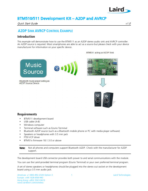
BTM510 511 开发套件 – A2DP 和 AVRCP 快速入门指南说明书
BTM510/511 Development Kit – A2DP and AVRCPQuick Start Guide v1.0 A2DP S INK AVRCP C ONTROL E XAMPLEIntroductionThis example will demonstrate how to use the BTM511 as an A2DP stereo audio sink and AVRCP controller. An A2DP source is required. Most smartphones are able to act as a source but please check with your device manufacturer for information on your specific device.Requirements▪BTM511 development board▪USB cable (A-B)▪Windows computer▪Terminal software such as Ezurio Terminal▪Bluetooth A2DP source (such as a Bluetooth mobile phone or PC with media player software)▪Speakers or headphones with 3.5 mm jack▪FTDI VCP driver▪BTM51x firmware 18.1.3.0 or aboveNote: Not all phones and computers support Bluetooth A2DP. Check with the manufacturer for A2DP support.The development board USB connector provides both power to and serial communications with the module. You can use the Laird-provided terminal program (Ezurio Terminal) or your own preferred terminal program.A set of stereo speakers or headphones should be plugged into the stereo out socket on the development board using a 3.5 mm audio jack.Device SetupTo set up the device, follow these steps:1.Install the FTDI VCP drivers on your PC.2.If not already installed, install your preferred terminal program.3.Connect the USB cable to the computer and development board. Ensure that the developmentboard switch is set to USB. Windows should find and install the development board as newhardware.4.Identify the virtual com port used by the development board using the device manager on aWindows computer.5.Connect the speakers to the development board 3.5 mm Stereo Out socket.6.Open the terminal program and select the virtual com port (9600 8N1) identified earlier.7.Check to be sure you can communicate by sending “at”. Once you press Enter, you should see OK.8.Send the commands as shown in Figure 1 to configure the BTM511. Refer to the user manual fordetailed command explanations.Notes: Commands are shown in lower case, responses from the BTM511 in upper case.If you power cycle the BTM511, the at+btp command must be resent. All other settings are storedin non-volatile memory.Figure 1: BTM511 Configuration CommandsYou may need to experiment with the ats515 setting depending on the device acting as a source; this is the Bluetooth Class of Device (COD) which describes the general characteristics and capabilities of a device. The COD does not reliably indicate which profiles or services are actually available. There are numerous possible combinations but typical values of ats515 could include $200400 (generic audio), $200414 (loudspeaker), and $200418 (headphones).Discovery and PairingThe BTM511 is now ready to be discovered by your Bluetooth A2DP source device.Because different devices handle pairing in different ways, it is not possible to provide step-by-step instructions for a specific device. Typically, you need to go to the device’s settings screen and select Bluetooth; this should allow you to search for and pair with the module.If your source device uses legacy pairing, you must enter the pairing PIN as 1234 on your source device when prompted. This PIN was previously setup on the BTM511 with the at+btk=<PIN> command.Source devices that support Bluetooth 2.1 (most recent smartphones do) use simple secure pairing (SSP). For these devices, you receive a prompt on both the source device and from the BTM511 as shown in Figure 2:Figure 2: SSP PromptsPAIR ? Indicates an incoming pair requestBCB1F3781D4F BT address of the source deviceGalaxy Nexus Its ‘friendly name’056029 A random six-digit number displayed on both devicesAccept the pairing request on the source device and then accept the pairing request on the BTM511 by sending at+btby, if required. Some devices may pair automatically without prompting depending on their security settings. The BTM511 pairing settings can be configured with various levels of security and user interaction. Please refer to the user manual for more details.A successful pairing is indicated by a PAIR 0 <remote device address> message.ConnectingAt this point you may see two connect messages: one for A2DP (UUID:0x110D) and one for AVRCP (UUID:0x110E). If the connect messages do not appear, you must manually connect from your source device; please refer to the manufacturer’s instructions if this issue occurs. Most smartphones will automatically connect.From your source device, begin audio streaming by opening the media player and playing a music track. You should hear the track from the speakers/headphones connected to the development board rather than from the source devices own internal speaker.Once the audio is streaming you will receive a message indicating the current sampling frequency (Figure 3).Figure 3: Current sampling frequencyIn this example:44100 Refers to 44100 khzINT Indicates that an internal codec is being usedFigure 4: Audio output gain and connection statusat+godControl the audio output gainat+gouati61 Sent to determine the status of the connection1 Indicates that A2DP is connectedRemote ControlAVRCP can be used to control the source device media player from the BTM511. See Figure 5.Figure 5: AVRCP Commandsat+avc45 Stop media playbackat+avc44 Start playbackFigure 6: Skip back and playback commandsat+avc4c Skip backat+avc46 Pause playbackNote: Not all commands may be supported by all devices.DisconnectingThe command ath* can be used to drop the all current Bluetooth connections. As each connection drops, a corresponding No Carrier message displays (Figure 7).Figure 7: Disconnection commandsResourcesFTDI Driver: /Drivers/VCP.htmEzurio terminal: /zips/Bluetooth%20Terminal%20Download.zipSupport: /Products/Wireless-M2M-and-Telematics-Solutions/Bluetooth-Module/ BTM511 User Manual: /WorkArea/linkit.aspx?LinkIdentifier=id&ItemID=5114R EVISION H ISTORY。
- 1、下载文档前请自行甄别文档内容的完整性,平台不提供额外的编辑、内容补充、找答案等附加服务。
- 2、"仅部分预览"的文档,不可在线预览部分如存在完整性等问题,可反馈申请退款(可完整预览的文档不适用该条件!)。
- 3、如文档侵犯您的权益,请联系客服反馈,我们会尽快为您处理(人工客服工作时间:9:00-18:30)。
BOOMTECH SEMICONDUCTORS CO.,LTD
Product Specification
Model : BT1213H
REV : V1.0
DRAWN BY :
CHECKED BY :
APPD BY:
1. Introduction
Boomtech Semiconductors Co., Ltd the pioneer of the Bluetooth 4.0 modules
BT1213H which is a high performance, cost effective, low power and compact solution. The Bluetooth module provides a complete 2.4GHz Bluetooth system
based on CSR 8635 chip which is a single-chip radio and baseband IC for Bluetooth 2.4GHz systems including basic rate, EDR to 3Mbps and Bluetooth low energy
2. Key Features
• Fully Qualified Single-chip Bluetooth® v4.0 System
•-91dBm (typical) π/4 DQPSK receiver sensitivity
and -81dBm (typical) 8DPSK receiver sensitivity
• A2DP v1.2, multipoint A2DP support enables connection to 2 A2DP
source devices for music playback
• CSR's latest CVC technology for narrowband and
wideband voice connections including wind noise reduction
• AVRCP v1.4
• Wideband speech supported by HFP v1.6 and mSBC codec
•Audio interfaces: I²S and PCM
• Stereo codec with 1 microphone input
• 5-band fully configurable EQ
• SBC, MP3 and AAC decoder support
• Wired audio support
Supported sample rates of 8, 11.025, 16, 22.05, 32,44.1, 48 and 96kHz (DAC only)
■Bluetooth low energy
• Dual-mode Bluetooth low energy radio
• Support for Bluetooth basic rate / EDR and low energy connections
• 3 Bluetooth low energy connections at the same time as basic rate A2DP
• Slim module with 24.5mm x 14.1mm x 2.0mm
• RoHS Compliant
3. Applications
• Stereo speakers
• Speakerphones
• Handsfree car kits
• 1-mic stereo headset or headphones
6. Module Package Information
6.1 Pinout Diagram and package dimensions 6.2 Module Pin descriptions
PIN NO.Pin Name
1
GND 2
UART_TX 3
UART_RX 4
UART_RTS 5
UART_CTS 6
PIO 7
PIO 8
PIO 9
PIO 10
SPI_EN 11PCM1_IN UART data output for debug only / PIO15 Ground Description UART data input for debug only / PIO14 UART request to send, active low / PIO16 UART clear to send,active low / PIO17 PCM1 synchronous data input/SPI_MOSI
for debug only for debug only SPI/PCM select input for debug only for debug only
12PCM1_CLK 13PCM1_OUT 14PCM1_SYNC
15RESET
16LED2(BLUE) 17LED1(RED) 18MFB/POWER 19CHARGE
20VBAT
211V8
22GND
23USB_N
24USB_P
25PIO7
26PIO/0
27PIO6
28PIO18
29PIO21
30LED3
31LINE/MIC_AN
32LINE/MIC_AP 33MIC_BIAS
34LINE_BN
35LINE_BP
36SPK_RN
37SPK_RP
38SPK_LN
39SPK_LP
40GND LINE/MIC_AP input positive
LINE_BN input negative
LINE_BP input positive
Microphone bias
Programmable input / output line 7
PCM1 synchronous data sync/SPI_CS
PCM1 synchronous data clock/SPI_CLK
PCM1 synchronous data output/SPI_MISO
LED driver(Open drain output)
LED driver(Open drain output)
Programmable input / output line 21
LINE/MIC_AN input negative
Programmable input / output line 18
LED driver(Open drain output)
Internal 1.8V
Power on/off input key indication
Reset if low. Input debounced so must be low for >5ms to cause a reset
Internal charger input for charging(5V)
Battery Power supply input for 3.0~4.2V
USB data minus
USB data plus with selectable internal
1.5kΩ pull-up resistor
Programmable input / output line 6
Ground
Programmable input / output line 0
Speaker output negative,right
Ground
Speaker output positive,right
Speaker output negative,left
Speaker output positive,left
7. Example Application Schematic。
