Circuit Modeling of Carbon Nanotube Interconnects and their Performance Estimation
碳纳米管电梯的作文

碳纳米管电梯的作文英文回答:Carbon nanotube (CNT) elevators are a theoretical means of vertical transportation that utilize the strength, flexibility, and electrical conductivity of carbon nanotubes (CNTs). CNTs are cylindrical structures made of carbon atoms arranged in a hexagonal lattice, and they possess remarkable mechanical and electrical propertiesthat make them promising materials for a wide range of applications, including energy storage, electronics, and transportation.The concept of CNT elevators was first proposed in 1999 by Richard Smalley and his colleagues at Rice University. They envisioned a system in which a series of CNT ropes would be suspended from a high-altitude platform, with a spacious cabin attached to the bottom of the ropes. The cabin would be powered by an electric motor, which would use the CNT ropes as electrical conductors to power theelevator up and down.CNT elevators offer several potential advantages over conventional elevators. First, CNTs are extremely strong and lightweight, so CNT ropes could be much longer and lighter than steel cables, allowing for the construction of elevators that are significantly taller than existing ones. Second, CNTs are good electrical conductors, so they could be used to power the elevator directly, eliminating the need for a separate power cable. Third, CNTs are flexible and elastic, so they could withstand high winds and earthquakes without breaking.However, there are also several challenges that must be overcome before CNT elevators can become a reality. First, CNTs are expensive to produce, so the cost of building a CNT elevator would be significantly higher than the cost of building a conventional elevator. Second, CNTs aresensitive to heat and moisture, so they would need to be protected from the elements in order to ensure their long-term durability. Third, CNTs can be damaged by electromagnetic fields, so they would need to be shieldedfrom sources of electromagnetic radiation.Despite these challenges, CNT elevators remain a promising concept with the potential to revolutionize vertical transportation. With continued research and development, it is possible that CNT elevators could one day become a reality, providing a safe, efficient, and environmentally friendly way to move people and goods up and down tall buildings.中文回答:碳纳米管电梯是一种理论上的垂直运输方式,它利用了碳纳米管(CNT)的强度、柔韧性和导电性。
纤维素模板法制备多孔碳纳米棒及其超级电容器性能(英文)
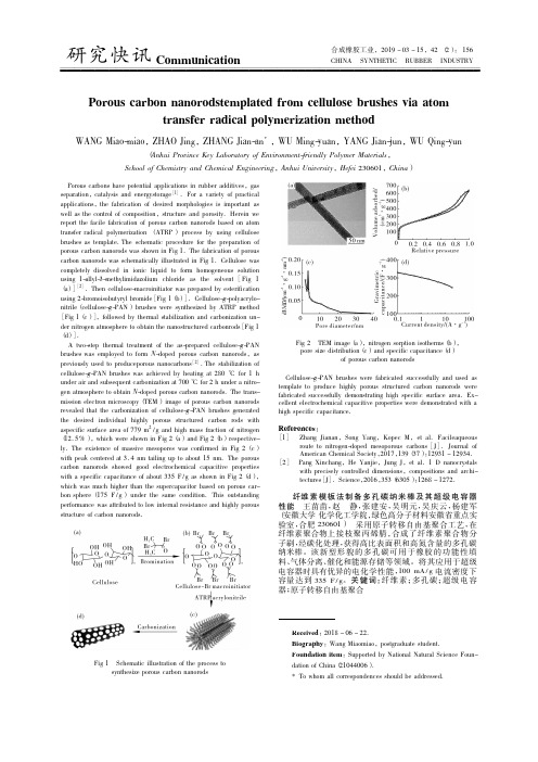
Porous carbons have potential applications in rubber additives,gas separation,catalysis and energystorage[1]. For a variety of practical applications,the fabrication of desired morphologies is important as well as the control of composition,structure and porosity. Herein we report the facile fabrication of porous carbon nanorods based on atom transfer radical polymerization ( ATRP ) process by using cellulose brushes as template. The schematic procedure for the preparation of porous carbon nanorods was shown in Fig 1. The fabrication of porous carbon nanorods was schematically illustrated in Fig 1. Cellulose was completely dissolved in ionic liquid to form homogeneous solution using 1-allyl-3-methylimidazolium chloride as the solvent [Fig 1 ( a) ][2]. Then cellulose-macroinitiator was prepared by esterification using 2-bromoisobutyryl bromide[Fig 1( b) ]. Cellulose-g-polyacrylonitrile( cellulose-g-PAN) brushes were synthesized by ATRP method [Fig 1( c) ],followed by thermal stabilization and carbonization under nitrogen atmosphere to obtain the nanostructured carbonrods[Fig 1 ( d) ].
The Physical Properties of Carbon Nanotubes
The Physical Properties of CarbonNanotubesCarbon nanotubes (CNTs) are one of the most fascinating materials developed in the past few decades. They are cylindrical nanostructures composed of carbon atoms arranged in a hexagonal pattern. CNTs have unique properties, including high strength and stiffness, small size, exceptional electrical conductivity, and thermal conductivity. These properties make them preferable for numerous applications in several fields, including electronics, materials science, aerospace, and biotechnology.Structure of carbon nanotubesCarbon nanotubes have two primary structural types: single-walled nanotubes (SWNTs) and multi-walled nanotubes (MWNTs). SWNTs consist of a single rolled sheet, while MWNTs contain multiple rolled sheets. The diameter of SWNTs ranges from 0.4to 2 nm, while MWNTs have diameters ranging from 2 to 100 nm. The length of CNTs is usually several micrometers, but they can be longer.Thanks to their small dimensions and tubular structure, CNTs have a high aspect ratio, which means that their length is much greater than their diameter. This aspect ratio gives CNTs their unique mechanical properties. They are exceptionally strong and stiff, with a Young's modulus three to four times higher than that of steel. Moreover, CNTs are quite resilient, and their deformation before failure is much more elevated than conventional materials, making them perfect for use in new structural materials.Electrical properties of carbon nanotubesOne of the most remarkable properties of CNTs is their electrical conductivity. They have excellent electrical properties, which means they can conduct electricity even better than copper. SWNTs are metallic or semiconducting depending on their chiral angle, while MWNTs are usually metallic.SWNTs have particular band structures, and their electrical properties depend heavily on their atomic structure. The electronic properties of CNTs make them ideal for use in electronic applications, such as field-effect transistors, diodes, and sensors. CNTs have the potential to improve the performance of transistors and other electronic devices significantly.Thermal properties of carbon nanotubesCNTs also have exceptional thermal conductivity, making them useful in thermal management materials. The thermal conductivity of CNTs is approximately seven times higher than that of copper. Moreover, CNTs are excellent heat conductors at the nanoscale, which gives them the potential to improve the efficiency of thermal management materials in electronic devices.Other physical properties of carbon nanotubesIn addition to their excellent mechanical, electrical, and thermal properties, CNTs also exhibit some other unique physical properties that make them advantageous for several applications. They are lightweight and can be dispersed in solvents, allowing them to be used in coatings, composites, and other materials.Furthermore, because of their nanoscale dimensions, CNTs have a high surface area-to-volume ratio, which makes them an effective adsorbent for gas and liquid molecules. This property makes CNTs promising candidates for gas storage and separation, as well as water purification.ConclusionCNTs are exceptional materials that have unique physical properties that lend themselves to several applications. They are lightweight, strong, stiff, and excellent electrical and thermal conductors, making them preferable for use in several fields, including electronics, materials science, and aerospace. Their physical properties make CNTs promising candidates for improving the performance of electronic devices, structural materials, and energy storage systems.。
Characterizing the properties of carbon nanotubes
Characterizing the properties ofcarbon nanotubesCarbon nanotubes (CNTs) have been the subject of extensive research due to their unique structural, electronic, mechanical, and thermal properties. CNTs are cylindrical tubes of carbon atoms, having a diameter of a few nanometers and a length of several micrometers. The walls of CNTs are made of graphene sheets that are rolled up into cylinders, resulting in a seamless tube with a hollow core. The properties of CNTs depend on their diameter, length, chirality, and defects, which can be controlled during the synthesis process.One of the most important properties of CNTs is their high aspect ratio, which is the ratio of their length to diameter. CNTs can have aspect ratios of up to 100,000, which makes them the strongest known materials, with tensile strengths up to 63 GPa. The strength of CNTs comes from their sp2 hybridized carbon bonds, which make the tubes extremely stiff and resilient. CNTs are also highly flexible, and can bend and twist without breaking, enabling them to be used in a wide range of applications.Another important property of CNTs is their electrical conductivity. CNTs are excellent conductors of electricity, with an electrical conductivity of up to 1x10⁷ S/m, which is higher than that of copper. The conductivity of CNTs is dependent on their diameter and chirality, with smaller diameter tubes being more conductive than larger diameter tubes. The high conductivity of CNTs makes them a promising material for electronic and optoelectronic applications, such as transistors, sensors, and solar cells.CNTs also possess exceptional thermal conductivity, which is the ability to conduct heat. CNTs have an extremely high thermal conductivity of up to 3500 W/mK, which is higher than that of any other known material. The high thermal conductivity of CNTs makes them ideal for use in thermal management applications, such as heat sinks and nanocomposites.Furthermore, CNTs are highly hydrophobic, meaning that they repel water. This property makes them useful in applications where water resistance is required, such as in coatings and membranes. CNTs are also resistant to chemical corrosion and oxidation, which makes them highly durable and long-lasting.However, CNTs also have some limitations that need to be addressed. One of the major challenges is their toxicity. While CNTs have shown great promise in medical applications, such as drug delivery and cancer therapy, their potential toxicity to cells and tissues is a cause of concern. Studies have shown that CNTs can cause lung damage and inflammation in rodents, raising questions about their safety for human use. Therefore, it is important to thoroughly evaluate the toxicity of CNTs before using them in biomedical applications.In conclusion, CNTs are a remarkable material with unique and exceptional properties that make them suitable for a wide range of applications. Their high strength, electrical and thermal conductivity, hydrophobicity, and chemical stability make them a promising material in the fields of electronics, energy, and healthcare. However, their potential toxicity needs to be addressed before they can be widely used in biomedical applications. Understanding the properties of CNTs is essential for developing new applications that can exploit their exceptional properties while minimizing their drawbacks.。
碳纳米管天梯一千字作文

碳纳米管天梯一千字作文English Answer:In the realm of nanotechnology, the concept of carbon nanotube space elevators has emerged as a futuristic and ambitious endeavor. Carbon nanotubes (CNTs), with their exceptional tensile strength and unique properties, have sparked the imagination of scientists and engineers, leading to the exploration of their potential for a revolutionary mode of transportation to the cosmos.The fundamental principle behind carbon nanotube space elevators involves the deployment of an extremely long and strong CNT cable stretching from the Earth's equator towards geostationary orbit, approximately 36,000 kilometers above sea level. This towering structure would serve as a vertical transportation system, enabling payloads to ascend and descend using electromagnetic propulsion or other novel techniques. The potential benefits are manifold, including lower launch costs,increased payload capacity, and enhanced accessibility to space for scientific research and exploration.However, realizing the vision of carbon nanotube space elevators presents formidable technological challenges. The foremost obstacle lies in the production of CNTs with the required length and strength. Current manufacturing techniques can produce CNTs on a limited scale, and scaling up the production process to generate kilometer-long CNTs remains a significant hurdle. Additionally, the harsh conditions of space, including exposure to extreme temperatures, radiation, and micrometeoroids, pose significant durability concerns for the CNT cable.Despite these challenges, research and development efforts continue to advance the field of carbon nanotube space elevators. Scientists are exploring innovative approaches to synthesize CNTs with enhanced properties and durability. Advancements in electromagnetic propulsion systems and the development of lightweight payloads are also key areas of research. International collaborations and public-private partnerships are fostering knowledgesharing and resource pooling to accelerate the realization of this ambitious concept.中文回答:碳纳米管太空电梯一千字作文。
碳纳米管天梯作文100

碳纳米管天梯作文100英文回答:Carbon nanotube elevator is a concept that has been proposed for space exploration and transportation. It involves the use of carbon nanotubes, which are cylindrical structures made of carbon atoms, to create a strong and lightweight material that can be used to build an elevator that reaches into space.One of the main advantages of a carbon nanotube elevator is its potential to revolutionize space travel. Currently, the cost of sending payloads into space is extremely high, mainly due to the need for large and powerful rockets. With a carbon nanotube elevator, the cost of reaching space could be significantly reduced, as it would eliminate the need for rockets altogether. This would open up new possibilities for scientific research, commercial activities, and even space tourism.Another advantage of a carbon nanotube elevator is its potential to make space exploration more accessible. Currently, only a select few astronauts have the opportunity to travel to space. However, with a carbon nanotube elevator, space travel could become more affordable and available to a larger number of people. This could lead to a greater understanding of our universe and the potential for new discoveries.Furthermore, a carbon nanotube elevator could also have environmental benefits. Traditional rocket launches contribute to air pollution and the emission of greenhouse gases. By using a carbon nanotube elevator, we could reduce our reliance on rockets and minimize the negative impact on our planet.中文回答:碳纳米管天梯是一个用于太空探索和交通的概念。
Carbon Nano-Tube 03版

Low density (1.3-1.4 g/cm3).
High resillence(回弹性).
8
Conclusions
CNTs phenomenal(显著的) mechanical properties, and unique electronic properties make them both interesting as well as potentially useful in future technologies.
9
Thank You!
School of Electronic Information Engi1n0 eering
SWCNT
MWCNT
4
Structure of SWCNTs
SWCNTs is classified according to how they are mapped into a single graphite(石墨) layer
There are 3 types of SWCNTs : 1> armchair nanotube (椅形C纳米管) 2> zigzag nanotube (锯齿形C纳米管) 3> chiral nanotube (手性C纳米管)
• The chemical bonding of CNT is composed entirely of sp2 bonds
3
Types of Carbon Nanotubes
• Single-walled carbon nanotubes (SWCNTs) • Multi-walled carbon nanotubes (MWCNTs)
5
COMSOL在介电泳数值模拟中的应用
Principle of DEP
Forπ ab 2ε m
12
α∇E 2
* ⎡ ⎤ ε * − εm p α = Re ⎢ * ⎥ * ε m + (ε * − ε m ) Lp ⎥ ⎢ p ⎣ ⎦
ε
* m, p
σ m. p = ε m, p − i ω
GEOMETRY MODELING
The model consists of the electrode, carbon nanotube and suspension. The contact resistance between carbon nanotube and electrode pad is far more larger than the resistance of carbon nanotube. Simplify the model of carbon nanotube.
Suspension
Carbon nanotube
Electrode Electrode
Substrate
GEOMETRY MODELING
We use rectangle as a carbon nanotube with wide of 2nm and length of 1um. The wide of electrode pad is 200nm.
S. Hee Won, H. Chang Soo, C, et al. “Controlled assembly of single CNTs bundle using Dielectrophoresis”, Microelectronic Engineering, 81, 2005: 83 ~ 89
and the relative permittivity is
- 1、下载文档前请自行甄别文档内容的完整性,平台不提供额外的编辑、内容补充、找答案等附加服务。
- 2、"仅部分预览"的文档,不可在线预览部分如存在完整性等问题,可反馈申请退款(可完整预览的文档不适用该条件!)。
- 3、如文档侵犯您的权益,请联系客服反馈,我们会尽快为您处理(人工客服工作时间:9:00-18:30)。
A Circuit Model for Carbon Nanotube Interconnects: ComparativeStudy with Cu Interconnects for Scaled TechnologiesArijit Raychowdhury and Kaushik Roy Dept of ECE, Purdue University, IN {araycho, kaushik}@Abstract: Semiconducting carbon nanotubes (CNTs) have gained immense popularity as possible successors to silicon as the channel material for ultra high performance field effect transistors. On the other hand, their metallic counterparts have often been regarded as ideal interconnects for the future technology generations. Owing to their high current densities and increased reliability, metallic-single walled CNTs (SWCNTs) have been subjects of fundamental research both in theory as well as experiments. Metallic CNTs have been modeled for RF applications in [1] using an LC model. In this paper we present an efficient circuit compatible R LC model for metallic SW CNTs, and analyze the impact of SW CNTs on the performance of ultra scaled digital VLSI design [2].I. INTRODUCTIONCarbon nanotubes [3] are sheets of graphite rolled into cylinders of diameters varying from 0.6nm to about 3nm. Depending on the direction in which they are rolled (called chirality), a CNT can be semiconducting with a distinct bandgap or it can be metallic with no bandgap. Metallic carbon nanotubes have been identified as a possible interconnect material of the future technology generations and be heir to Al and Cu interconnects. Leading theoreticians as well as experimentalists have started research in the earnest to understand the transport mechanisms and the conducting properties of the metallic CNTs [4]. Both single-walled carbon nanotubes (SWCNTs) as well as multi-walled carbon nanotubes (MWCNTs) are being investigated for performance and scalability. It has been demonstrated that MWCNTs are diffusive and have high IR drops whereas in SWCNTs, ballistic transport (drift) can be achieved and would be suitable for interconnect designs. However, in both SWCNTs and MWCNTs, very high current densities have been noted with very little performance degradation. For example, Wei et al.[5] showed that the current carrying capacity of CNTs did not degrade after 350h at current densities of ~1010 A/cm 2 at 250 °C. The thermal conductivity of CNTs [6] is about 1700–3000 W/m K. In this paper, for the first time, we envisage a realistic scenario where carbon nanotube interconnects with their intrinsic resistances and capacitances and the extrinsic (or parasitic)capacitances and inductances have been evaluated for performance. We have compared the performance of metallic SWCNTs with scaled Cu interconnects. We have used an RLC based circuit-compatible model for Cu interconnects. In the practical scenario, a damascene process is used in Cu technology to make narrow trenches and fill it up with Cu. This results in reduced interconnect dimensions and high scalability. However, it comes with the price of increased surface and grain boundary scattering. These effects have been introduced in our circuit compatible model of Cu interconnects. II. MODELING CARBON NANOTUBE INTERCONNECTSLet us consider a system of parallel carbon nanotubes, as shown in fig. 1a. Let the radius of the nanotubes be r , the separation betweennanotubes be d and let the length of a nanotube be l . We can describe the interconnect behavior of the nanotube as that of a transmission line with an RLC model as illustrated in fig. 1b and proposed in [1]. However, in [1] the diffusive component, R was not modeled and was taken to be in the ballistic limit. In such a case, the intrinsic impedance (also called the contact or quantum resistance) is given by h/ e 2 where e is the electronic charge and h is Plank's constant [7]. However, this is an optimistic assumption and under high bias or long interconnects lengths, electron-phonon interactions start to play an important role and the effects of scattering need to be incorporated.In the next three subsections, we will elaborate the R, L and C models used in our simulations.A. ResistanceRecent experiments by Ji-Yong Park et. al. [8] have measured the dc resistance of SW metallic CNTs of diameter 1.8nm (r=0.9nm). In this incoherent limit for four such channels of conduction, the differential resistance of a nanotube of length l (> Ȝ) is given by [7]: O l e h dI dV R diff ¸¹·¨©§ 24(1) where, V is the applied voltage, I is the current thorugh the CNT and Ȝ is the mean free path (mfp ). If l < Ȝ, the resistance is aconstant given by the quantum resistance for four channels (h/4e 2). The value of Ȝ is given by the scattering mechanism and isdependant on the length of the nanotube and the applied bias. For low biases (V critical <160mV), the principle scattering mechanism is due to acoustic phonons having a mfp of about 1.6µm (Ȝacc ). For higher supply biases the optical phonon (Ȝop ~ 200nm) and zone boundary phonon (Ȝzo ~30nm) scattering becomes dominant. Thus it is evident that the resistance of a CNT will be a function of thebias voltage (V bias ) as well as the length. Hence depending on the bias, the differential resistance can be expressed as:R LC Q C C(a) (b)Fig. 1: (a) Geometry of CNT (b) RLC model of parallel CNTsWe have validated this resistance model described by (2) against recently published experimental data. Fig. 2 shows how the proposed model corroborates with experimental data presented in [8] both for high as well as low voltage biases.It should be noted that eqn. (2) describes the differential resistanceof a metallic CNT. It is necessary to obtain the net (or dc)resistance of the CNT. Hence the overall dc resistance (the ratio ofthe total current, I net to the corresponding bias voltage V bias ) can bewritten as: Thus we have developed a length and bias dependant piecewise linear resistance model which has been verified with experimental data. For short lengths of the nanotube, under small bias voltages, the quantum resistance limit (or, ballistic transport) can be reached. However, for longer lengths of the current saturates to a constant value of around 25P A. We have used this resistance model forcircuit simulations using SPICE.B. InductanceTo obtain the inductance of the CNT we follow the procedure explained in reference [1,9]. Let us first consider the magnetic inductance between a CNT and the ground plane. In the presence of a ground plane, the magnetic inductance per unit length is given by [9] :This is calculated by relating the total magnetic energy and relatingit to the current flowing in the wire. For a typical situation, thenanotube is on top of an insulating (typically silicon-dioxide)substrate, with a conducting medium below. A typical oxide thickness is between 10nm and 1 P m whereas a typical nanotube radius of 1nm-2 nm. It can be noted that the magnetic inductance isa relatively weak function of the factor (h/d ) and for typical geometries it can be estimated to be around 1nH/P m.For one dimensional conductors, the kinetic inductance is as important as the magnetic inductance. The details of its derivation can be found in [1]. The kinetic inductance is given byHence, in the transmission line model (fig. 1b) we have consideredkinetic inductance only (L = L kinetic ) and have neglected magnetic inductance.C. Capacitance For CNT interconnects laid down in parallel, two distinctcapacitances would be important. One of them is the couplingelectrostatic capacitance, C C and the other is the quantum capacitance of the metallic nanotube. Equating this with the energy stored in the quantum capacitance we obtain [9]Apart from the quantum capacitance, the electrostatic capacitance is also important in parallel layout of CNT interconnects. The coupling capacitance between two CNTs each of radius r laid out at a distance d between them is given byThus we have a complete RLC model for the CNT interconnects.II. MODELING Cu INTERCONNECTSFor V< V critical: ¸¸¹·¨¨©§4¸¹·¨©§ low low diffl e h dI dV RO 24For V> V critical¸¸¹·¨¨©§4¸¹·¨©§ high highdiffl eh dI dV RO 24 where,1)( 4x for x<1=x otherwise Ȝlow = Ȝacc and Ȝhigh = (Ȝop -1+ Ȝzo -1)-1. (2a) (2b)(a) (b)Fig. 2: Differential resistance of a CNT : Validation of the proposed model with experimental data [8] : (a) for low bias (b) for high biasFor V< V critical: low diff low R RFor V> V critical 11)11( ¸¸¸¹·¨¨¨©§high diff high diff low diff bias critical highR R R V V R(3a) (3b) ¸¹·¨©§ d h L magnetic2cosh 21S P(4)F kinetic v e h L 22 ~ 16nH/µm(5) F Q hv e C 22 ~ 100 aF/µm(6) ¸¸¹·¨¨©§ ¸¹·¨©§122ln 2r d r dlC C HS(7)For the purpose of comparison, we have also modeled and simulated Cu interconnects (fig 3).A. ResistanceGrain boundary and surface scattering effects have been incorporated in a manner described in [4] to determine the resistivity of copper. The surface scattering effects can be modeled using a correction term to the intrinsic resistivity of Cu. The size dependant resistivity is given by [11]11531111)1(231 f»¼º«¬ª ¸¹·¨©§ ³dt pe e t t p k ktkt i size U U (8) where k is the ratio of the film thickness (h cu ) and the electron mean free path and p (0 p 1) is the surface scattering coefficient. Similarly the grain boundary scattering can be included in the resistivity model using13211ln 21313 »¼º«¬ª D D D D U U i grain R Rd g 1O D (9)where d g is the grain diameter, Ȝ is the electron mean free path and R (0 R 1) is the grain boundary reflection coefficient. In a manner described in [11] we have assumed p=0.6 and R=0.4. The grain boundary is also assumed to be equal to the width of the copper wire and hence d g = w cu . Hence the total resistance of each Cu wire is given byB. CapacitanceThe coupling capacitance between adjacent copper wires is given by the simple parallel plate capacitance formula)(cu cu C w d lh C H (10)C. Inductance The self inductance and mutual inductances of the Cu interconnects have been determined using the software tool MIND [12]. It involves calculation of the magnetic energy of a set of parallel wires and equating the total magnetic energy with that stored in an equivalent inductance. The details of the derivation can be found in [12] and will not be discussed here.Thus we have developed an equivalent RLC model for Cu interconnects and this has been used in comparing performance of Cu interconnects vis-à-vis CNT interconnects.III. SWITCHING DELAY USING SINGLE AND MULTIPLE CARBON NANOTUBESIn the next few sections, we will estimate the switching delay of a CNT interconnect and compare it with traditional Cu interconnect. Also the implications of scaling on CNT interconnects will bediscussed. A Single CNT interconnect First, let us consider a single CNT used as an interconnect.Consider a step input of maximum voltage 500mV to such a CNT. Fig. 4 shows the switching delay as a function of length for a single CNT interconnect. It can be noted that the switching delay for the CNT is several orders of magnitude higher than that predicted by ITRS. This is due to the large resistance of a single CNT. Even for perfect contacts and at low bias the minimum resistance of a CNT interconnect is h/(4e 2), which is approximately 6K ȍ. This resistance increases as the length of the interconnect increases and as the voltage across the CNT exceeds V critical . As a result the switching delay increases fast and far exceeds the ITRSprediction. Hence we conclude from here that a single CNT would be insufficient to act as a high speed interconnect for the future technology.B. Parallel CNT interconnectsThe next logical step would be to use CNTs in parallel that can be used to route a single signal. The corresponding layout is demonstrated in fig. 5 where N x parallel interconnects have been used as a single effective interconnect wire. It has been noted earlier that CNTs have a typical current handling capacity of 25uA/nanotube. Let us consider a current requirement of 500uA. Hence we would require 20 nanotubes in parallel (N x = 20). With a spacing of 2r (r=1.8nm) between the nanotubes, it will take a width(w = 2r(N x -1)) of 80nm. For comparison, let us consider a copper interconnect of the same width (w cu = 80nm). The maximum current handling capacity ismuch lower (J max ~ 106A/cm 2). However, the damascene process allows making deep trenches and using copper interconnects which are far deeper than they are wide. In our example, for a J maxofFig. 4: Delay vs. length of a single CNT interconnect. The ITR S prediction has been marked. Note: The length of the CNT is in meters.w cuh cuFig. 3: Layout of parallel Cu interconnects showing the interconnect dimensions. Note that h cu is the height of a Cu wire whereas h is its height from the ground plane.106A/cm2 the height, h cu needs to be 625nm in order to supply 500uA. This aspect ratio of 1:8 is easily possible in Cu technologies.Fig. 6, shows the switching delay of 20 parallel CNT interconnects and the copper interconnect (w cu = 80nm and h cu = 625nm). It can be noted that the CNT has a much higher switching delay than copper, in spite of its higher current density. This apparently counter-intuitive result can be easily understood by noting that:x Practical complementary MOS circuits are voltage driven and not current driven. In other words, the capacitors (gatecapacitance + parasistics) are charged through resistivepaths by a constant voltage source (V dd).x In voltage driven circuits the resistance of the interconnect wire and not its current density is important for performance.An ideal current source can pump a high current throughthe small cross-sectional area of the CNT. However, theresistance offered by the CNT is intrinsically high andcontrols the RLC switching delay.x The damascene process allows a high aspect ratio (ratio of h cu to w cu) of the Cu interconnects which substantiallyreduces the resistance of the Cu wire.It should thus be noted that for a voltage driven circuit the interconnect resistance and not the current density determines the switching speed.C. Oscillator frequencyIn the previous sub-sections we have considered the RLC switching delay of CNT interconnects and compared with Cu. Now let us consider a three-stage ring oscillator [13] made of scaled silicon MOSFETs. Simulations have been carried out using BPTM MOSFET models of 45nm channel length [14]. Fig. 11 shows the effect of interconnects on the frequency of oscillation.It can be observed that CNT interconnects can reduce the frequency of oscillation by orders of magnitude if the interconnect is longer than 1µm. For shorter interconnects the degradation of performance is small. If parallel CNTs are used then the effective interconnect resistance reduces. However the resistance offered by Cu interconnects is orders of magnitude smaller than CNT and it has been shown in fig. 11.IV. CONCLUSIONThis paper, for the first time, provides a realistic RLC model for CNT interconnects. Inspite of the high current density, CNT interconnects suffer from very high intrinsic resistance and kinetic inductance and severely limits high frequency of operation. Performance can be improved by routing the same signal through parallel CNTs. It has been shown that it requires a substantial increase in the number of metal layers to meet the performance of copper in the same die area. Thus CNTs provide reliable interconnect solutions but are limited in terms of performance in the high performance digital VLSI.References:[1]P. J. Burke, ‘An RF circuit model for carbon nanotubes’, IEEETrans. On Nanotech, Vol 2(1), March 2003, pp: 55-58[2]International Technology Roadmap for Semiconductors/[3]M. S. Dresselhaus et. al., Carbon nanotubes: Synthesis, structure,properties and applications, Springer, 2001.[4]Jun Li et. al., ‘Bottom-up approach for carbon nanotubeinterconnects’, Applied Physics Letters, Vol 82(15), April 2003.[5] B. Q. Wei et. al., Applied Phys. Letters. Vol 79, 1172, 2001.[6]J. Hone et. al., Physical Review. B, Vol 59, R2514, 1999.[7]S. Datta, Electronic transport in mesoscopic systems, CambridgeUniversity Press, 1995.[8]Ji-Yong, et. al., ‘Electron-Phonon scattering in metallic single-walled carbon nanotubes’ cond-mat/0309641, Sept. 28, 2003.[9]Burke, ‘Luttinger liquid theory as a model of the gigahertz electricalproperties of carbon nanotubes’, IEEE Trans. On Nanotech, Vol1(3), Sept. 2002, pp: 129-144.[10]M.W. Bockrath, “Carbon nanotubes electrons in one dimension,”Ph.D. dissertation, Univ. California, Berkeley, CA, 1999.[11]Wen Wu et. al., “Studies on size effects of copper interconnectlines’, Proc of Solid-State and Integrated-Circuit Technology, Vol. 1,Oct 2001 pp:416 – 418.[12]Zhong et. al, Proc. of Int. Conf. on Comp Design, pp. 428-433, 2002.Fig. 5: Layout of parallel CNTs. N X CNTs have been used to route the same signal. Only the 1st and the N x th CNTfeels the coupling capacitor C CFig. 6: Comparison of delay of 20 parallel CNT interconnects with copper interconnect having the same equivalent width (w=80nm). Note: The interconnect length is in meters. Fig. 7: The effect of interconnect on the oscillation frequency of a three-stage ring oscillator. Note how the CNT interconnects degrade the performance because of their high intrinsic resistance.。